

Mitsubishi MGFC44V3436 Datasheet
3.4~3.6GHz BAND 25W INTERNALLY MATCHED GaAs FET
DESCRIPTION
The MGFC44V3436 is an internally impedance matched
GaAs power FET especially designed for use in 3.4~3.6
GHz band amplifiers. The hermetically sealed metal-ceramic
package guarantees high reliability.
FEATURES (TARGET)
Class A operation
Internally matched to 50 (Ω) system
High output power
P1dB=25W (TYP.) @f=3.4~3.6GHz
High power gain
GLP=12dB (TYP.) @f=3.4~3.6GHz
High power added efficiency
P.A.E.=36% (TYP.) @f=3.4~3.6GHz
Loe distortion [item -51]
IM3= -45dBc (TYP.) @Po=33.5dBm S.C.L.
APPLICATION
item 01 : 3.4~3.6GHz band power amplifier
item 51 : 3.4~3.6GHz band digital radio communication
MITSUBISHI SEMICONDUCTOR <GaAs FET>
MGFC44V3436
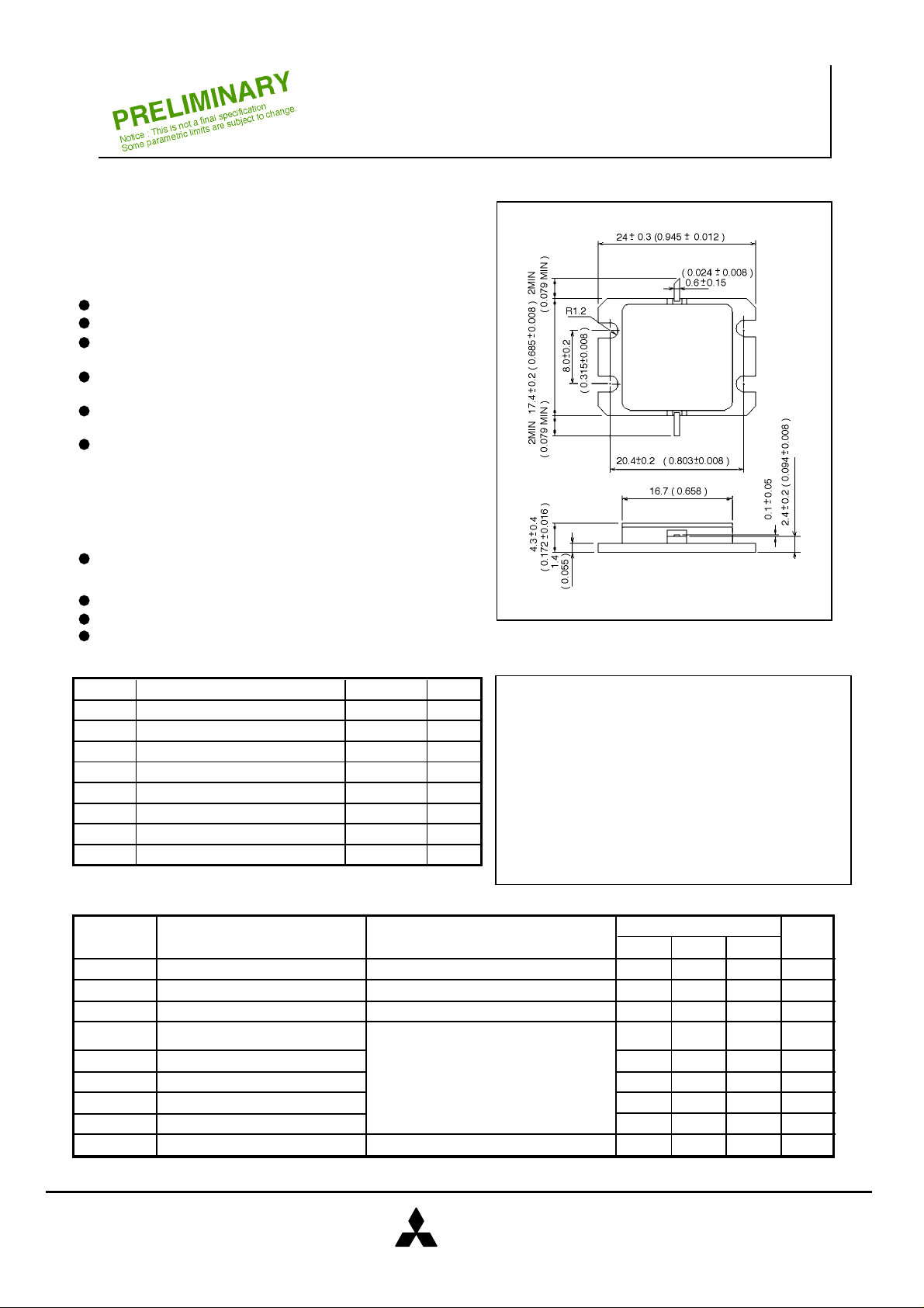
OUTLINE DRAWING
Until : millimeters (inches)
(1)
(2)
(3)
QUALITY GRADE
IG
RECOMMENDED BIAS CONDITIONS
VDS=10V
ID=6.4A
RG=25Ω
GF-38
ABSOLUTE MAXIMUM RATINGS (Ta=25°C)
Symbol
VGDO
VGSO
ID
IGR
IGF
PT
Tch
Tstg
*1 : Tc=25°C
Gate to drain voltage -15 V
Reverse gate current
Forward gate current 126 mA
Total power dissipation
Channel temperature
Storage temperature
Parameter Ratings Unit
*1
125 W
175
-65 ~ +175 °C
-15Gate to source voltage
20Drain current
-60
V
A
mA
°C
< Keep safety first in your circuit designs! >
Mitsubishi Electric Corporation puts the maximum effort into
making semiconductor products better and more reliable,
but there is always the possibility that trouble may occur
injury, fire or property damage. Remember to give due
consideration to safety when making your circuit designs,
with appropriate measures such as (i)placement of
substitutive, auxiliary circuits, (ii)use of non-flammable
material or (iii)prevention against any malfunction or mishap.
ELECTRICAL CHARACTERISTICS (Ta=25°C)
Symbol Parameter
Saturated drain current VDS=3V, VGS=0VIDSS 18—
VGS (off)
P1dB
GLP
ID
P.A.E. Power added efficiency 36
IM3 *2
Rth (ch-c) Thermal resistance
*2 : item-51, 2 tone test, Po=33.5dBm Single Carrier Level, f=3.4, 3.5, 3.6GHz, ∆f=10MHz
*3 : Channel to case
Transconductance VDS=3V, ID=6.4Agm 6.5— —
Gate to source cut off voltage VDS=3V, ID=120mA V
Output power at 1dB gain
compression
Linear power gain 12 —
Drain current
3rd order IM distortion
VDS=10V, ID (RF off)=6.4A, f=3.4-3.6GHz
∆Vf method
*3
Test conditions
MITSUBISHI
ELECTRIC
(1) GATE
(2) Source (FLANGE)
(3) DRAIN
Limits
Min. Typ. Max
—
-5
—
—
—
—
1.2
as of Feb.'98
43
11
—
—
-42
—
—-2
44 dBm
6.4
-45
—
Unit
A
S
dB
A
%
dBc
°C/W
 Loading...