m
< C band internally matched power GaAs FET >
MGFC42V5964A
5.9 – 6.4 GHz BAND / 16W
DESCRIPTION
The MGFC42V5964A is an internally impedance-matched
GaAs power FET especially designed for use in 5.9 – 6.4
GHz band amplifiers. The hermetically sealed metal-ceramic
package guarantees high reliability.
FEATURES
Internally matched to 50(ohm) system
High output power
P1dB=16W (TYP.) @f=5.9 – 6.4GHz
High power gain
GLP=9.0dB (TYP.) @f=5.9 – 6.4GHz
High power added efficiency
P.A.E.=33% (TYP.) @f=5.9 – 6.4GHz
Low distortion [item -51]
IM3=-45dBc (TYP.) @Po=31.0dBm S.C.L
APPLICATION
item 01 : 5.9 – 6.4 GHz band power amplifier
item 51 : 5.9 – 6.4 GHz band digital radio communication
QUALITY
IG
RECOMMENDED BIAS CONDITIONS
VDS=10V ID=4.5A RG=25ohm Refer to Bias Procedure
OUTLINE
N
I
M
2
R1. 2
2
2
.
.
0
0
-
-
/
/
+
+
4
0
.
.
7
8
1
N
I
M
2
4
.
0
-
/
+
3
.
4
4
.
1
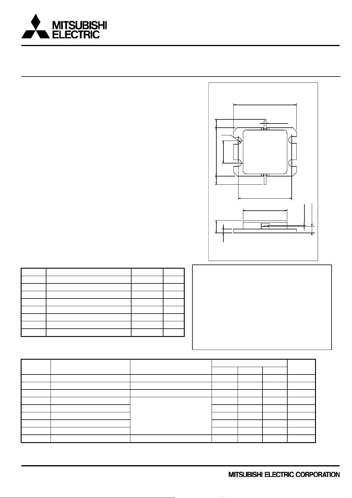
GF-38
24 +/- 0.3
(1)
20.4 +/- 0.2
16.7
0.6 +/- 0.15
(3)
(1) gate
(2) source(flange)
(3)drain
Absolute maximum ratings (Ta=25C)
Symbol Parameter Ratings Unit
VGDO
VGSO Gate to source breakdown voltage -15 V
ID Drain current 15 A
IGR Reverse gate current -40 mA
IGF Forward gate current 84 mA
PT *1 Total power dissipation 93.7 W
Tch Cannel temperature 175 C
Tstg Storage temperature -65 to +175 C
*1 : Tc=25C
Gate to drain
breakdown voltage -15 V
Electrical characteristics
(Ta=25C)
Symbol Parameter Test conditions Limits Unit
IDSS
gm
VGS(off)
P1dB
GLP Linear Power Gain 8 9 - dB
ID Drain current - 4.5 - A
P.A.E. Power added efficiency - 33 - %
IM3 *2 3rd order IM distortion
Rth(ch-c) *3
Saturated drain current VDS=3V,VGS=0V - 9
Transconductance VDS=3V,ID=4.4A - 4
Gate to source cut-off voltage VDS=3V,ID=80mA -2 -3 -4 V
Output power at 1dB gain compression
Thermal resistance delta Vf method - - 1.6
*2 :item -51 ,2 tone test,Po=31.0dBm Single Carrier Level ,f=6.4GHz,delta f=10MHz
*3 :Channel-case
VDS=10V,ID(RF off)=4.5A
f=5.9 – 6.4GHz
Keep Safety first in your circuit designs!
Mitsubishi Electric Corporation puts the maximum
effort into making semiconductor products better
and more reliable , but there is always the
possibility that trouble may occur with them.
Trouble with semiconductors may lead to personal
injury , fire or property damage. Remember to give
due consideration to safety when making your
circuit designs , with appropriate measure such
as (I) placement of substitutive , auxiliary circuits ,
(ii) use of non-flammable material or (iii) prevention
against any malfunction or mishap.
Min. Typ. Max.
12 A
- S
41.5 42.5 - dBm
-42 -45 - dBc
(2)
C/W
uni t : m
5
2
.
0
.
0
0
-
/
-
/
+
+
4
.
1
.
2
0
Publication Date : Apr., 2011
1

< C band internally matched power GaAs FET >
MGFC42V5964A
5.9 – 6.4 GHz BAND / 16W
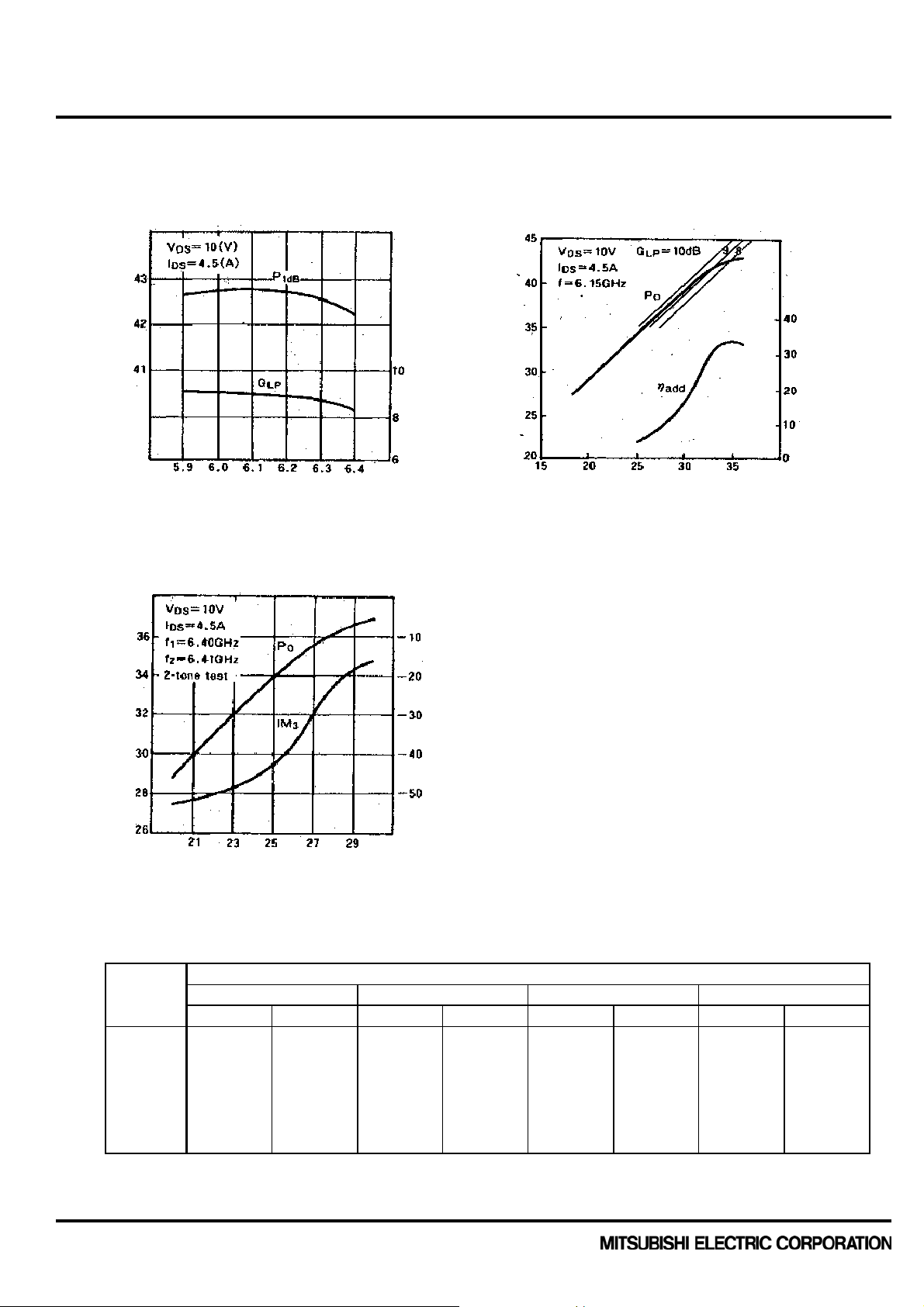
MGFC42V5964A TYPICAL CHARACTERISTICS( Ta=25deg.C )
OUTPUT POW ER P1dB(dBm)
P1dB,Glp VS. f Po,Eadd VS. Pin
LINEA R POWER GAIN Glp(dB )
OUTP UT POWER Po(dBm)
POWER ADDED EFFICIENCY Eadd(%)
FREQUENCY f (GHz) INPUT POWER Pin(dBm)
Po,IM3 VS. Pin
IM3(dBc)
OUT PUT POWER Po(dBm S.C .L)
INPUT POWER Pin(dBm S.C.L.)
MGFC42V5964A S-parameters( Ta=25deg.C , VDS=10(V),IDS=4.5(A) )
fS
(GHz) Magn. Angle(deg.) Magn. Angle(deg.) Magn. Angle(deg.) Magn. Angle(deg.)
5.90 0.36 82 2.99 -74 0.071 -133 0.26 80
6.00 0.35 56 2.95 -91 0.071 -151 0.32 72
6.10 0.35 34 2.91 -108 0.072 -167 0.35 65
6.20 0.35 14 2.88 -124 0.078 177 0.37 58
6.30 0.34 -4 2.81 -140 0.079 161 0.41 53
6.40 0.33 -23 2.72 -157 0.079 146 0.43 48
11
S Parameters (TYP.)
S
21
S
12
S
22
Publication Date : Apr., 2011
2
 Loading...