DESCRIPTION
The MGFC42V3436 is an internally impedance-matched
GaAs power FET especially designed for use in 3.4 - 3.6
GHz band amplifiers. The hermetically sealed metal-ceramic
package guarantees high reliability.
FEATURES
Class A operation
Internally matched to 50(ohm) system
High output power
P1dB = 16W (TYP.) @ f=3.4 - 3.6 GHz
High power gain
GLP = 13 dB (TYP.) @ f=3.4 - 3.6GHz
High power added efficiency
P.A.E. = 37 % (TYP.) @ f=3.4 - 3.6GHz
Low distortion [item -51]
IM3=-45dBc(Min.) @Po=32dBm S.C.L.
APPLICATION
item 01 : 3.4 - 3.6 GHz band power amplifier
item 51 : 3.4 - 3.6 GHz band digital ratio communication
QUALITY GRADE
IG
RECOMMENDED BIAS CONDITIONS
VDS = 10 (V)
ID = 4.5 (A)
RG=25 (ohm)
MITSUBISHI SEMICONDUCTOR <GaAs FET>
MGFC42V3436
3.4 - 3.6GHz BAND 16W INTERNALLY MATCHED GaAs FET
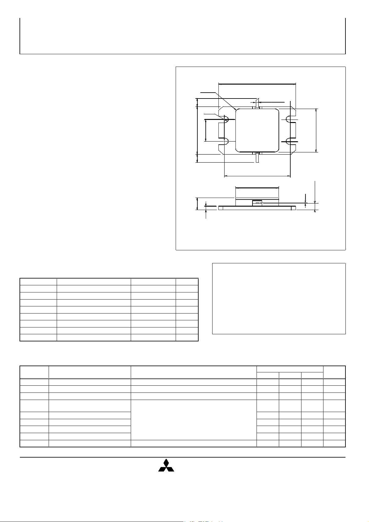
OUTLINE DRAWING Unit: millimeters
24+/-0.3
R1.25
GF-18
N
I
3
M
2
.
2
.
0
0
R1.2
-
-
/
/
+
+
4
0
.
.
7
8
1
N
I
M
2
4
.
0
/
+
0
.
4
4
.
1
(1)
0.6+/-0.15
(3)
20.4+/-0.2
13.4
(1): GATE
(2): SOURCE (FLANGE)
(3): DRAIN
8
.
5
(2)
1
2
.
0
/
+
4
1
.
.
2
0
ABSOLUTE MAXIMUM RATINGS
(Ta=25deg.C)
Symbol Parameter Ratings Unit
VGDO Gate to drain voltage -15 V
VGSO Gate to source voltage -15 V
ID Drain current 12 A
IGR Reverse gate current -40 mA
IGF Forward gate current 84 mA
PT Total power dissipation *1 78.9 W
Tch Channel temperature 175 deg.C
Tstg Storage temperature -65 / +175 deg.C
*1 : Tc=25deg.C
ELECTRICAL CHARACTERISTICS
(Ta=25deg.C)
Symbol Parameter Test conditions
IDSS
gm
VGS(off)
P1dB
GLP
ID
P.A.E.
IM3
Rth(ch-c)
*1 : item -51, 2 tone test, Po=32dBm Single Carrier Level, f=3.6GHz, delta f=5MHz
*2 : Channel-case
Saturated drain current
Transconductance
Gate to source cut-off voltage
Output power at 1dB gain
compression
Linear power gain
Drain current
Power added efficiency
3rd order IM distortion *1
Thermal resistance *2
VDS = 3V , VGS = 0V - 11 - A
VDS = 3V , ID = 4.4A - 4 - S
VDS = 3V , ID = 80mA - - -4.5 V
VDS=10V, ID(RF off)=4.5A, f=3.4 - 3.6GHz 12 13 - dB
delta Vf method - - 1.9
Mitsubishi Electric Corporation puts the maximum effort into
making semiconductor products better and more reliable,
but there is always the possibility that trouble may occur
with them. Trouble with semiconductors may lead to personal
injury, fire or property damage. Remember to give due
consideration to safety when making your circuit designs,
with appropriate measures such as (1)placement of
substitutive, auxiliary circuits, (2)use of non-flammable
material or (3)prevention against any malfunction or mishap.
MITSUBISHI
ELECTRIC
< Keep safety first in your circuit designs! >
Limits Unit
Min. Typ. Max.
41.5 42.5 - dBm
- 4.5 - A
-37- %
-42 -45 - dBc
deg.C/W
Sep. 1998

TYPICAL CHARACTERISTICS
(
)
MITSUBISHI SEMICONDUCTOR <GaAs FET>
MGFC42V3436
3.4 - 3.6GHz BAND 16W INTERNALLY MATCHED GaAs FET
Ta=25deg.C
45
VDS=10(V)
IDS=4.5(A)
44
P1dB
43
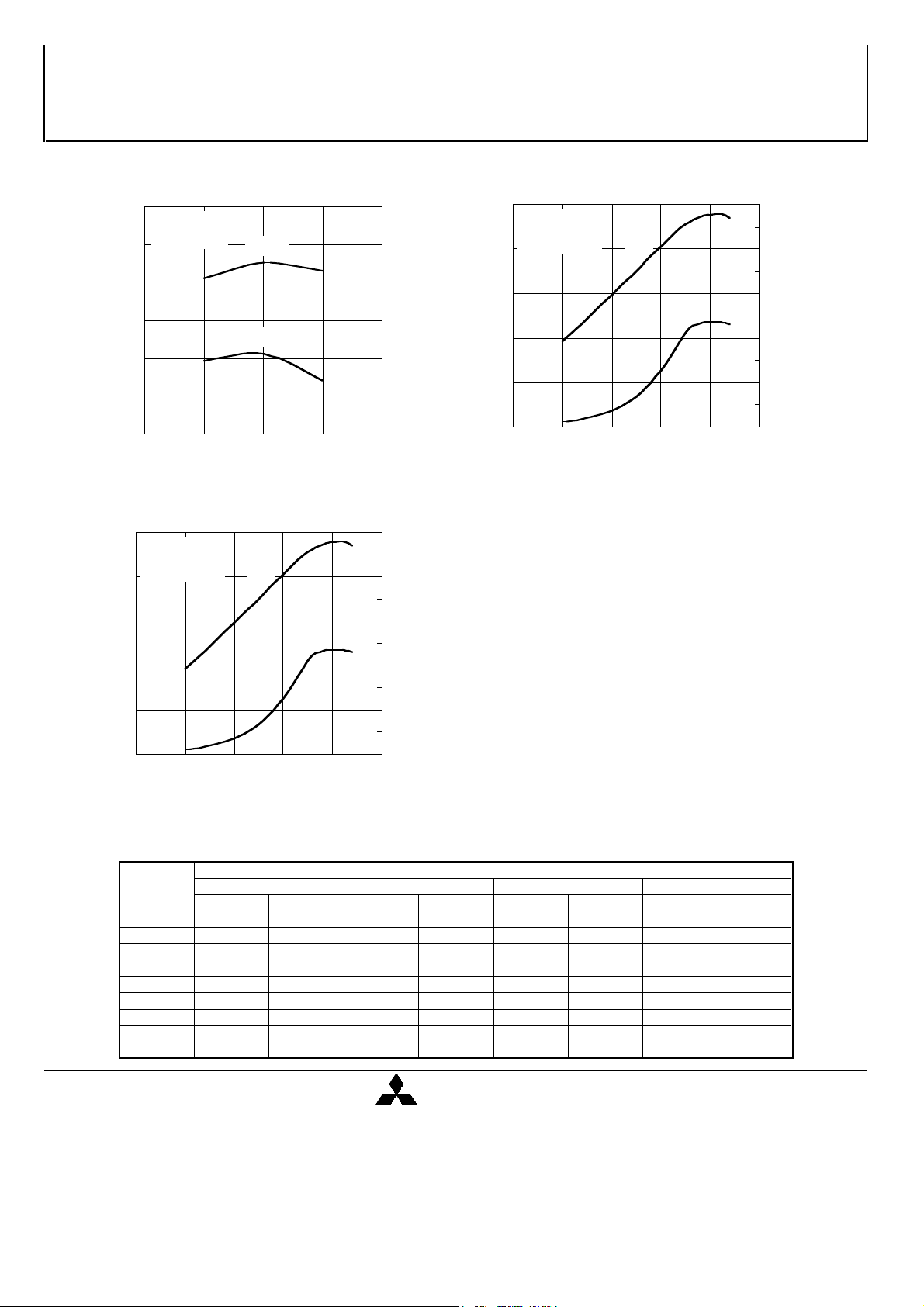
P1dB,GLP vs. f
42
OUTPUT POWER P1dB (dBm)
GLP
41
40
39
3.3 3.4 3.5 3.6 3.7
FREQUENCY f(GHz)
Po,PAE vs. Pin
45
VDS=10(V)
IDS=4.5(A)
f=3.5(GHz)
40
Po
35
OUTPUT POWER Po(dBm)
30
PAE
25
20
10 15 20 25 30 35
19
18
17
45
40
35
OUTPUT POWER Po(dBm)
16
30
15
25
14
LINEAR POWER GAIN GLP(dB)
13
20
100
90
80
70
60
50
40
30
20
10
POWER ADDED EFFICIECY PAE(%)
0
Po,PAE vs. Pin
VDS=10(V)
IDS=4.5(A)
f=3.5(GHz)
Po
PAE
10 15 20 25 30 35
INPUT POWER Pin (dBm)
100
90
80
70
60
50
40
30
20
10
POWER ADDED EFFICIECY PAE(%)
0
INPUT POWER Pin (dBm)
S parameters ( Ta=25deg.C , VDS=10(V),IDS=4.5(A) )
S-Parameters (TYP.)
f S11 S21 S12 S22
(GHz) Magn. Angle(deg) Magn. Angle(deg) Magn. Angle(deg) Magn. Angle(deg)
3.30
3.35
3.40
3.45
3.50
3.55
3.60
3.65
3.70
0.43 -19 4.592 133 0.04 74 0.40 10
0.30 -56 5.044 112 0.05 55 0.31 -14
0.25 -80 5.124 103 0.05 42 0.26 -26
0.23 -138 5.188 82 0.06 21 0.20 -59
0.30 -179 5.114 63 0.06 4 0.18 -96
0.36 154 4.895 45 0.06 -20 0.19 -129
0.39 143 4.758 37 0.06 -29 0.20 -139
0.42 126 4.546 21 0.06 -43 0.24 -157
0.43 118 4.433 14 0.06 -52 0.25 -163
MITSUBISHI
ELECTRIC
Sep. 1998
 Loading...