

MITSUBISHI SEMICONDUCTOR <GaAs FET>
MGFC41V5964
5.9 - 6.4GHz BAND 12W INTERNALLY MATCHED GaAs FET
DESCRIPTION
The MGFC41V5964 is an internally impedence matched
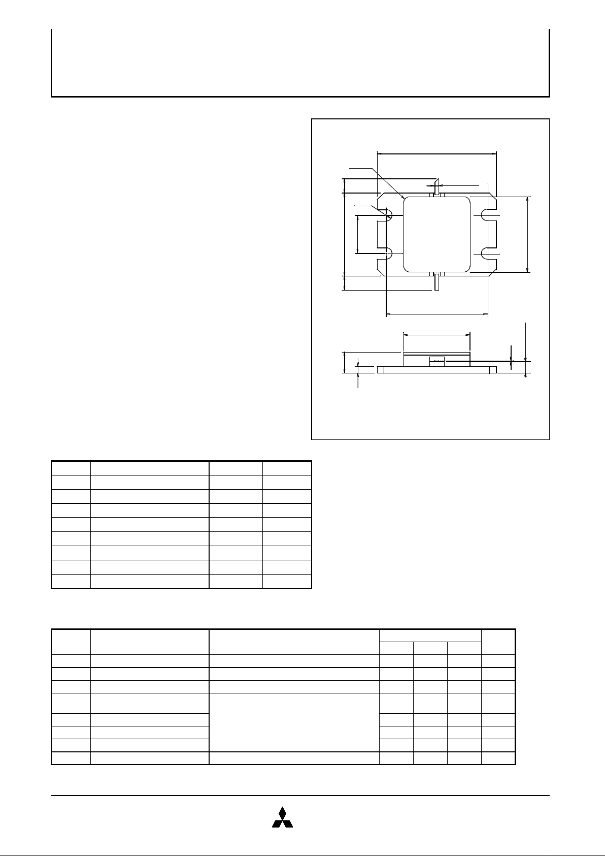
OUTLINE DRAWING
Unit: millimeters (inches)
GaAs power FET especially designed for use in 5.9 - 6.4
GHz band amplifiers. The hermetically sealed metal-ceramic
package guarantees high raliability.
FEATURES
Internally matched to 50ohm system
High output power
P1dB = 12W (TIP.) @ f=5.9 - 6.4 Hz
High power gain
GLP = 9.5 dB (TYP.) @ f=5.9 - 6.4 GHz
High power added efficiency
Eadd = 33 % (TYP.) @ f=5.9 - 6.4 GHz
Low Distortion[Item-51]
IM3=-45 dBc(TYP.)@Po=30dBm S.C.L.
APPLICATION
5.9 - 6.4GHz band amplifiers
QUALITY GRADE
IG
RECOMMENDED BIAS CONDITIONS
VDS = 10V
(1): GATE
ID = 3.4 A
(2): SOURCE (FLANGE)
Rg = 50(ohm) Refer to Bias Procedure
GF-18
(3): DRAIN
ABSOLUTE MAXIMUM RATINGS
Symbol Parameter Ratings Unit
V
GDO
Gate to drain voltage -15 V
V
GSO
Gate to source voltage -15 V
I
D
Drain current 12 A
I
GR
Reverse gate current -30 mA
I
GF
Forward gate current 63 mA
P
T
Total power dissipation *1 53.6 W
Tch Channel temperature 175 DegreesC
Tstg Storage temperature -65 to +175 DegreesC
*1 : Tc=25 DegreesC
ABSOLUTE MAXIMUM RATINGS
Symbol Parameter Test conditions
Limits
Unit
Min Typ Max
IDSS Saturated drain current VDS = 3V , VGS = 0V - - 12 A
gm Transconductance VDS = 3V , ID = 3.0A - 3 - S
VGS(off) Gate to source cut-off voltage VDS = 3V , ID = 30mA - - -5 V
P1dB
Output power at 1dB gain
compression
40 41 - dBm
GLP Linear power gain VDS = 10V , ID = 3.4A , f = 5.9 - 6.4 GHz 8.5 9.5 - dB
Eadd Power added efficiency - 33 - %
IM3 *2 3rd order IM distortion -42 -45 - dBc
Rth(ch-c) Thermal resistance *1 Delta Vf method - - 2.8 C/W
*1 : Channel to case
*2 : Item-51,2tone test,Po=30dBm Single Carrier Level,f=6.4GHz,Delta f=10MHz
MITSUBISHI
ELECTRIC
4.0+/-0.4
1.4
2MIN
2.4+/-0.2
0.1
17.4+/-0.3
R1.25
2MIN
0.6+/-0.15
(1)
24+/-0.3
20.4+/-0.2
13.4
(3)
8.0+/-0.2
R1.2
15.8
(2)
MITSUBISHI SEMICONDUCTOR <GaAs FET>
MGFC41V5964
5.9-6.4GHz BAND 12W INTERNALLY MATCHED GaAs FET
TYPICAL CHARACTERISTICS
(Ta=25 DegreesC)
S PARAMETERS
(Ta=25 DegreesC , VDS=10V , IDS=3.4A)
S Parameters (TYP.)
f
S
11
S
21
S
12
S
22
(GHz) Magn. Angle(deg.) Magn. Angle(deg.) Magn. Angle(deg.) Magn. Angle(deg.)
5.9 0.37 124 2.98 -81 0.051 -131 0.31 111
6.0 0.35 105 2.94 -96 0.053 -145 0.31 102
6.1 0.32 84 2.91 -112 0.058 -163 0.30 94
6.2 0.29 64 2.88 -128 0.060 -177 0.29 87
6.3 0.25 38 2.86 -144 0.064 167 0.26 82
6.4 0.23 8 2.83 -161 0.066 152 0.22 81
MITSUBISHI
ELECTRIC
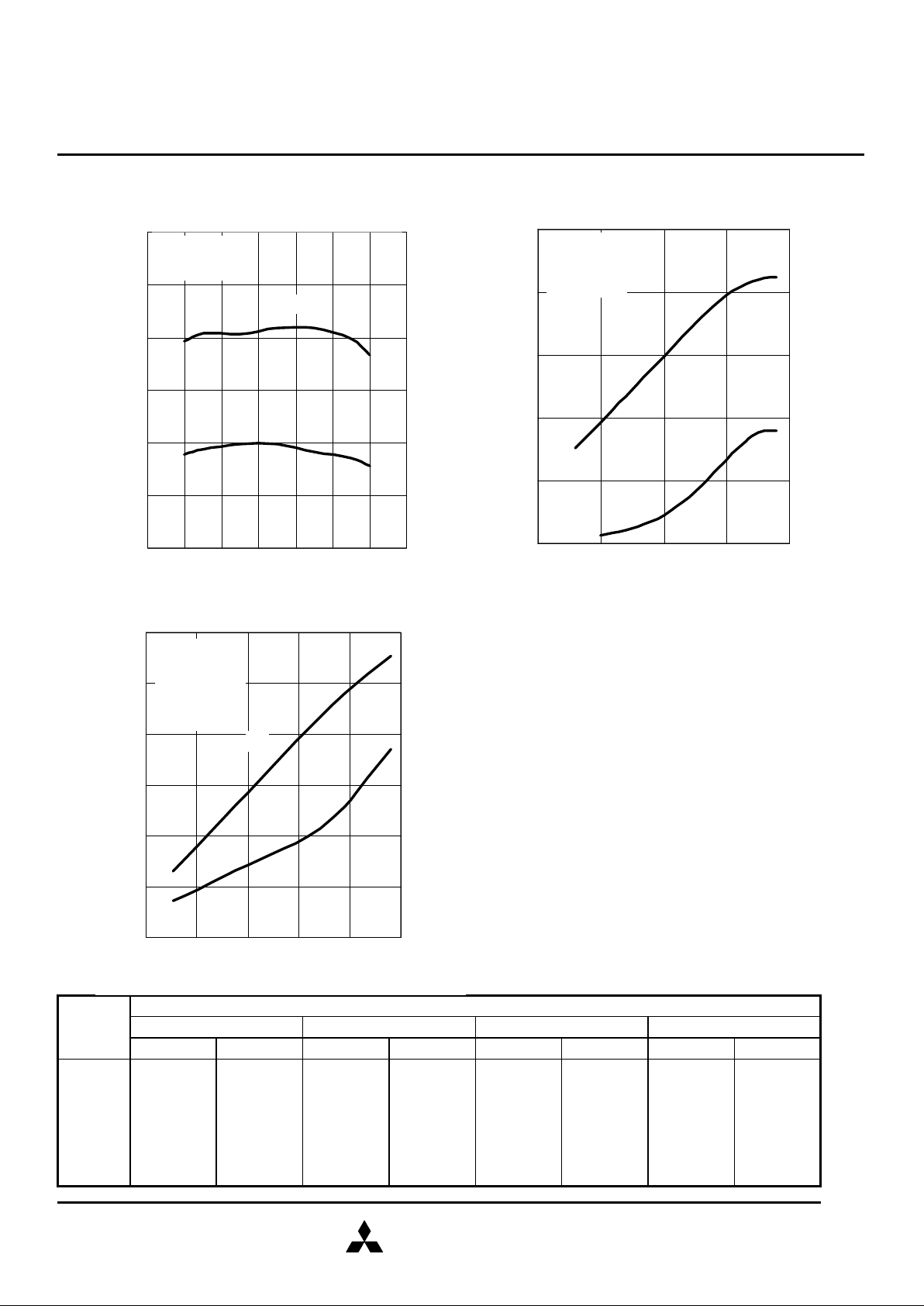
Po,Eadd vs. Pin
20
25
30
35
40
45
15 20 25 30 35
I NPUT POWER Pin (dBm)
OUTPUT POWER Po (dBm)
0
20
40
60
80
100
VDS=10
V
VDS=10V
ID=3.4A
f=6.15GHz
Po
Eadd
POWER A DDED EF FICIENCY E add (%)
Po,IM3 vs. Pin
24
26
28
30
32
34
36
17 19 21 23 25 27
I NPUT POWER Pin (dBm) S.C.L.
OUTPUT POWER Po (dBm) S.C.L.
-60
-50
-40
-30
-20
-10
0
IM3
Po
IM3 (dBc)
VDS=10V
IDS=3.4A
f=6.4 G H z
Delta f =10 MHz
2-to ne test
P1dB,GLP vs. f
37
38
39
40
41
42
43
5.8 5.9 6.0 6.1 6.2 6.3 6.4 6.5
FREQUENCY f (GHz)
OUTPUT POWER P1dB (dBm)
6
8
10
12
14
16
18
LIN EAR POWER GA IN GLP (dB)
VDS=10V
ID=3.4A
P1dB
GLP
 Loading...