

Mitsubishi MGF7168C Datasheet
Technical Note
Specifications are subject to change without notice.
MITSUBISHI SEMICONDUCTOR<GaAsMMIC>
MGF7168C
UHF BAND GaAs POWER AMPLIFIER
DESCRIPTION
MGF7168C is a monolithic microwave integrated
circuit for use in UHF-band power amplifier.
FEATURES
- Low voltage operation
Vd=3.2V
- High output power
Po=33dBm (typ.) @1710~1785MHz
Po=33dBm (typ.) @1850~1910MHz
- High efficiency
Id=1250mA (typ. ) @Po=33dBm
- Small size
6.1x7.0x1.10mm
- Surface mount package
- 2 Stage Amplifier
- External matching circuit is required
APPLICATION
- 1.8GHz band handheld phone
- 1.9GHz band handheld phone
QUALITY GRADE
- GG
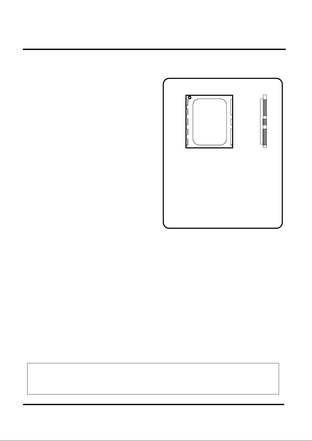
PIN CONFIGURATION (TOP VIEW)
Pi
Vg1
Vd1
R
Vg2
: RF input (Note1)
Pin
: RF output (Note1)
Pout
: Drain bias 1
Vd1
: Drain bias 2
Vd2
: Gate bias 1
Vg1
: Gate bias 2
Vg2
: Connect to GND
GND
: Connect to GND
CASE
: Connect to GND through
R
the resistor
Note1: Connect to matching circuits.
GND
GND
Vd2 / Po
*Mitsubishi Electric Corporation puts the maximum effort into making semiconductor products better and reliable, but there
is always the possibility that trouble may occur with them. Trouble with semiconductors may lead to personal injury, fire or
property damage. Remember to give due consideration to safety when making your circuit designs, with appropriate
measures such as (i) placement of substitutive, auxiliary, circuits, (ii) use of non-flammable material or (iii) prevention
against any malfunction or mishap.
MITSUBISHI ELECTRIC
(1/12)
Mar.'97
MITSUBISHI SEMICONDUCTOR<GaAsMMIC>
UHF BAND GaAs POWER AMPLIFIER
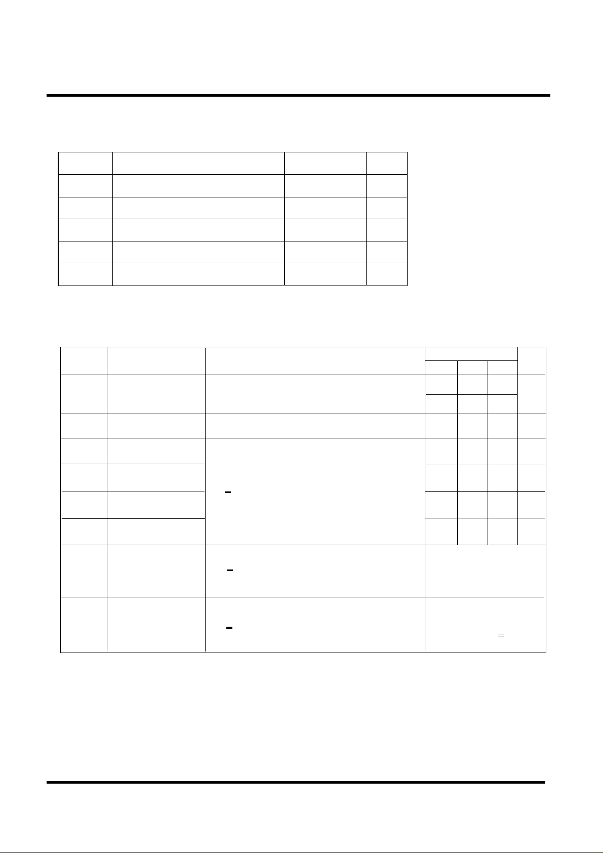
ABSOLUTE MAXIMUM RATINGS
Symbol Parameter Ratings Unit
MGF7168C
Vd1,Vd2
Vg1,Vg2
Pi
Tc(op)
Tstg
Drain voltage
Gate voltage
Input power
Operating case temperature
Storage temparature
ELECTRICAL CHARACTERISTICS (Ta=25˚C)
Symbol
f
Pin
Idt
Ig
2sp
Parameter
frequency
Input power
Total drain current
Gate current
2nd harmonics
Vd1=Vd2=3.2V,Po=33dBm
Vd1=Vd2=3.2V,
Pin<10dBm,
Po=33dBm
Test conditions
6
-4
15
-30~+85
-30~+100
V
V
dBm
˚C
˚C
Note1,2
Limits
MIN TYP MAX
1710 1785—
1850 1910
— 10
—
— —
—
—
—
—
—
Unit
MHz
dBm
mA1250
mA3
dBc-30
ρin
—
—
Note1 : Electrical characteristics are changed by the external matching circuit.
Limits are guaranteed by using MITSUBISHI test fixture.
Note2 : GMSK Pulse operation
Note3 : Sampling inspection
input VSWR
Damage
with-standing
Stability
Note3
Note3
Vd1=Vd2=3.2V,
Pin<10dBm,
Load VSWR=10, All phase
Time=10 sec
Vd1=Vd2=3.2V,
Pin<10dBm,
Load VSWR=3:1, All phase
MITSUBISHI ELECTRIC
(2/12)
— —
No damage
No oscillation
Spurious level<-60dBc
3
Mar.'97
—
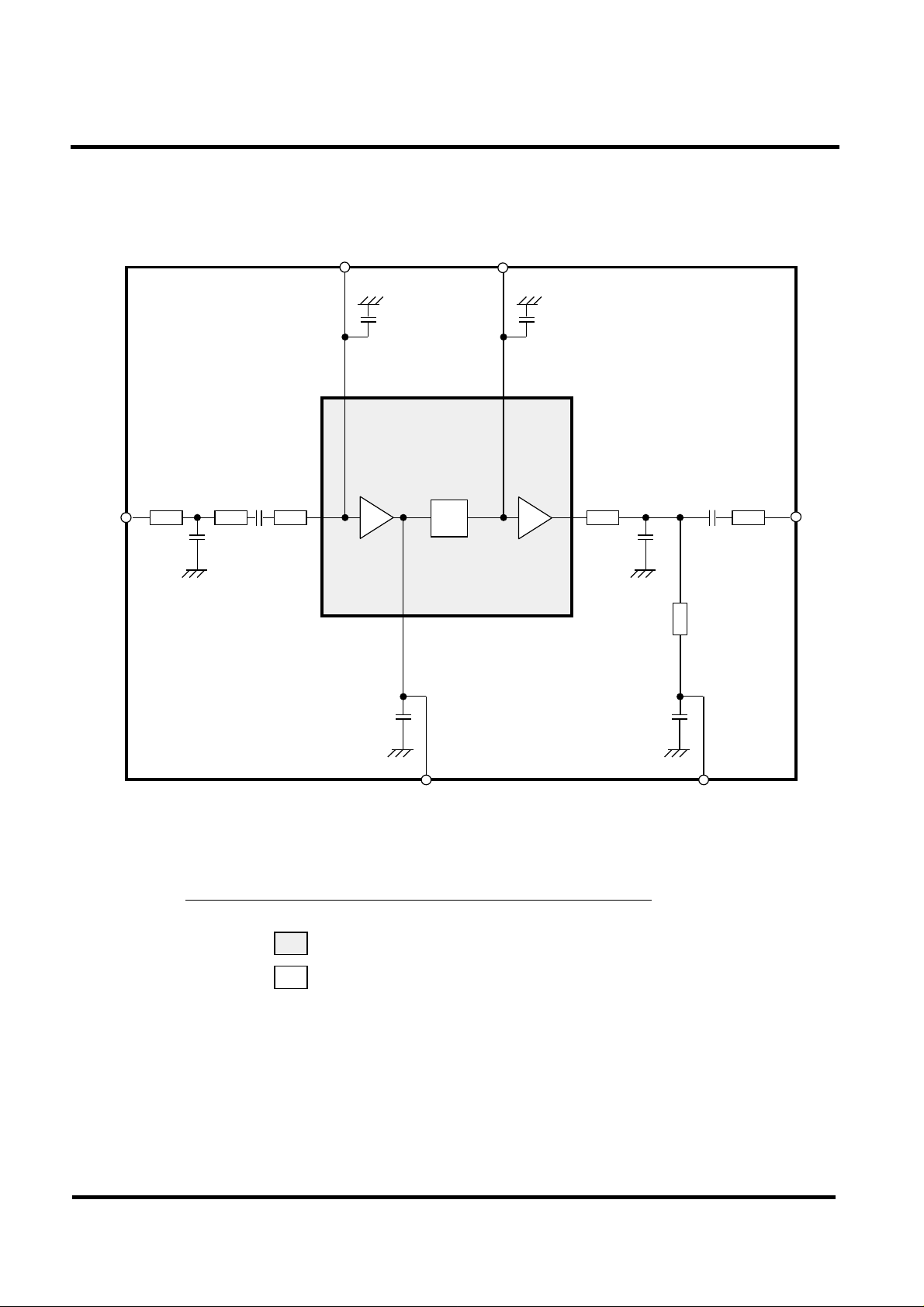
MITSUBISHI SEMICONDUCTOR<GaAsMMIC>
VG1 VG2
MGF7168C
UHF BAND GaAs POWER AMPLIFIER
Pin
FET1
Matching
circuits
FET2
VD1 VD2
Equivalent circuit of MGF7168C with our test board
: MGF7168C(Ceramic package)
Pout
: our test board(εr=4.8, t=0.6mm)
MITSUBISHI ELECTRIC
(3/12)
Mar.'97
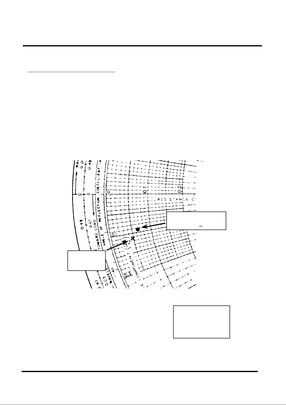
Input/Output Impedance
ZI=4.5-j27.8 (Ω) : 1.88GHz
ZL(ηmax) = 3.3-j4.7 (Ω) : f=1.88GHz
ZL(Po max)= 2.4-j5.8 (Ω) : f=1.88GHz
MITSUBISHI SEMICONDUCTOR<GaAsMMIC>
MGF7168C
UHF BAND GaAs POWER AMPLIFIER
Pomax
(33.8dBm)
ηmax
1150mA(Po>32.8dBm)
Conditions;
Vd1=Vd2=3.2V
Vgg=-2.0V
Pin=10dBm
MITSUBISHI ELECTRIC
(4/12)
Mar.'97
 Loading...