

Page 1
MITSUBISHI SEMICONDUTOR <GaAs FET>
without permission by Mitsubishi Elec
Trouble with semiconductors may lead to personal
Feb./2007
SUPER LOW NOISE InGaAs HEMT
MGF4961B
DESCRIPTION
The MGF4961B super-low noise HEMT (High Electron Mobility
Transistor) is designed for use in K band amplifiers.
FEATURES
Low noise figure @ f=20GHz
NFmin. = 0.7dB (Typ.)
High associated gain @ f=20GHz
Gs = 13.5dB (Typ.)
APPLICATION
C to K band low noise amplifiers
QUALITY GRADE
GG
RECOMMENDED BIAS CONDITIONS
VDS=2V , ID=10mA
MITSUBISHI Proprietary
Not to be reproduced or disclosed
ORDERING INFORMATION
Tape & reel 4000pcs./reel
ABSOLUTE MAXIMUM RATINGS
Symbol Parameter Ratings Unit
V
GDO
V
GSO
ID
PT Total power dissipation 50 mW
Tch
T
stg
Gate to drain voltage -4 V
Gate to source voltage -4 V
Drain current IDSS mA
Channel temperature 125 °C
Storage temperature -55 to +125 °C
(Ta=25°C )
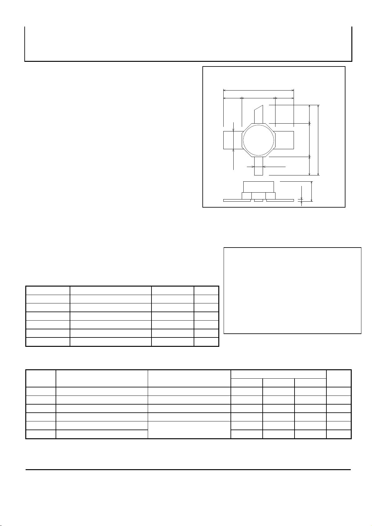
Outline Drawing
4.0±0.2
(1.05)
②
1.02±0.1
GD-31
Keep Safety first in your circuit designs!
Mitsubishi Electric Corporation puts the maximum
effort into making semiconductor products better
and more reliable , but there is always the
possibility that trouble may occur with them.
injury , fire or property damage. Remember to give
due consideration to safety when making your
circuit designs , with appropriate measure such
as (I) placement of substitutive , auxiliary circuits ,
(ii) use of non-flammable material or (iii) prevention
against any malfunction or mishap.
1.9±0.1
①
③
tric
0.5±0.1
(1.05)
(unit: mm)
(1.05)
4.0±0.2
②
(1.05) 1.9±0.1
① Gate
② Source
±0.05
0.125
1.19±0.2
③ Drain
ELECTRICAL CHARACTERISTICS
Synbol Parameter Test conditions
V
(BR)GDO
I
GSS
I
DSS
V
GS(off)
Gs
NFmin.
Gate to drain breakdown voltage
Gate to source leakage current
Saturated drain current
Gate to source cut-off voltage
Associated gain
Minimum noise figure
(Ta=25°C )
IG=-10µA
VGS=-2V,VDS=0V
VGS=0V,VDS=2V
VDS=2V,ID=500µA
VDS=2V,ID=10mA
f=20GHz
MITSUBISHI
(1/4)
Limits Unit
MIN. TYP. MAX
-3 -- -- V
-- -- 50 µA
15 -- 60 mA
-0.1 -- -1.5 V
11.5 13.5 -- dB
-- 0.70 0.95 dB
Page 2
MITSUBISHI SEMICONDUTOR <GaAs FET>
V
Feb./2007
SUPER LOW NOISE InGaAs HEMT
MGF4961B
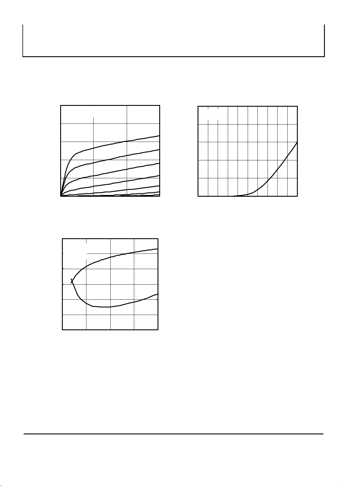
TYPICAL CHARACTERISTICS
50
40
(mA)
D
I
30
20
10
=-0.1V/STEP
GS
ID vs. V
DRAIN CURRENT
0
0 1 2 3
Drain to Source voltage VDS(V)
1.6
VDS=2V
f =20GHz
1.4
1.2
, NF (dB)
1.0
0.8
NOISE FIGURE
0.6
0.4
0 5 10 15 20
NF
DRAIN CURRENT, ID (mA)
DS
NF & Gs vs. I
Gs
(Ta=25°C)
D
16
14
12
10
8
6
4
ID vs. V
50
VDS=2V
40
(mA)
D
30
20
10
DRAIN CURRENT, I
0
-1.0 -0.5 0.0
Gate to Source voltage, VGS(V)
Gs(dB)
ASSOCIATED GAIN,
GS
MITSUBISHI
(2/4)
Page 3

MITSUBISHI SEMICONDUTOR <GaAs FET>
Freq.RnNFmin
(GHz)
(mag)
(ang)
(dB)
26
0.350
89.9
0.51
1.20
Γ
opt
Feb./2007
S PARAMETERS
Freq. S22
SUPER LOW NOISE InGaAs HEMT
(Ta=25°C,VDS=2V,ID=10mA)
S11 S21 S12
MGF4961B
(GHz) (mag) (ang) (mag) (ang) (mag) (ang) (mag) (ang)
1 0.991 -16.4 4.743 162.8 0.015 76.9 0.658 -13.0
2 0.967 -32.5 4.652 146.3 0.028 66.2 0.643 -25.8
3 0.928 -48.5 4.525 129.9 0.041 54.8 0.622 -38.9
4 0.886 -64.5 4.403 113.8 0.052 43.4 0.596 -51.4
5 0.835 -80.3 4.252 98.3 0.059 33.1 0.571 -63.0
6 0.782 -98.8 4.089 81.6 0.065 21.3 0.541 -76.5
7 0.729 -115.0 3.885 66.6 0.068 11.7 0.517 -87.6
8 0.682 -130.4 3.665 52.2 0.067 2.6 0.492 -98.0
9 0.637 -145.0 3.437 39.2 0.066 -6.2 0.474 -106.1
10 0.563 -155.8 3.265 28.3 0.063 -15.5 0.461 -116.0
11 0.536 -165.2 3.248 17.1 0.051 -21.9 0.461 -121.0
12 0.527 -175.0 3.266 5.0 0.043 -19.3 0.479 -128.9
13 0.520 172.8 3.303 -8.4 0.047 -17.7 0.480 -139.8
14 0.509 160.4 3.422 -21.6 0.047 -15.3 0.487 -147.7
15 0.474 145.5 3.542 -36.3 0.044 -19.1 0.489 -157.0
16 0.459 129.1 3.659 -52.3 0.052 -15.0 0.482 -167.4
17 0.449 104.5 3.881 -68.5 0.058 -26.7 0.488 -177.8
18 0.445 74.9 4.101 -89.4 0.062 -44.4 0.473 164.4
19 0.473 40.8 4.063 -111.4 0.059 -68.0 0.402 143.4
20 0.534 8.1 3.940 -134.0 0.052 -93.8 0.325 118.7
21 0.597 -21.4 3.685 -157.2 0.050 -125.1 0.251 86.6
22 0.657 -44.1 3.324 179.7 0.046 -155.7 0.198 46.3
23 0.695 -64.0 2.969 158.8 0.058 169.5 0.216 3.2
24 0.696 -79.4 2.570 138.3 0.065 148.6 0.247 -27.3
25 0.686 -93.5 2.294 119.4 0.082 128.7 0.289 -45.2
26 0.656 -105.2 2.038 100.1 0.095 118.8 0.346 -56.5
NOISE PARAMETERS
12 0.525 144.8 0.08 0.43
13 0.462 166.2 0.09 0.47
14 0.403 -174.0 0.11 0.51
15 0.348 -155.5 0.12 0.55
16 0.297 -138.3 0.13 0.58
17 0.249 -122.1 0.14 0.61
18 0.204 -106.8 0.15 0.64
19 0.186 -72.3 0.19 0.67
20 0.168 -39.5 0.23 0.70
21 0.223 -14.6 0.29 0.80
22 0.276 17.5 0.35 0.89
23 0.296 36.8 0.39 0.97
24 0.315 55.2 0.43 1.05
25 0.333 72.9 0.47 1.13
Note) Rn is normalized by 50ohm
(VDS=2V,ID=10mA, Ta=25°C)
MITSUBISHI
(3/4)
Reference point
S parameter measurement:
Board: εr=2.6
Thickness = 0.4mm
4-φ0.3TH
0.4TH
(Unit: mm)
1.90
0.31
0.61
2.5
0.48
0.135
1.1
Page 4

MITSUBISHI SEMICONDUTOR <GaAs FET>
Feb./2007
SUPER LOW NOISE InGaAs HEMT
Requests Regarding Safety Designs
Mitsubishi Electric constantly strives to raise the level of its quality and reliability. Despite these concerted efforts,
however, there will be occasions when our semiconductor products suffer breakdowns, malfunctions or other problems.
In view of this reality, it is requested that every feasible precaution be taken in the pursuit of redundancy design,
malfunction prevention design and other safety-related designs, to prevent breakdowns or malfunctions in our products
from resulting in accidents involving people, fires, social losses or other problems, thereby upholding the highest levels of
safety in the products when in use by customers.
Matters of Importance when Using these Materials
1. These materials are designed as reference materials to ensure that all customers purchase Mitsubishi Electric
semiconductors best suited to their specific use applications. Please be aware, however, that the technical information
contained in these materials does not comprise consent for the execution or use of intellectual property rights or other
rights owned by Mitsubishi Electric Corporation.
2. Mitsubishi Electric does not assume responsibility for damages resulting from the use of product data, graphs, charts,
programs, algorithms or other applied circuit examples described in these materials, or for the infringement of the
rights of third-party owners resulting from such use.
3. The data, graphs, charts, programs, algorithms and all other information described in these materials were current at
the issue of these materials, with Mitsubishi Electric reserving the right to make any necessary updates or changes in
the products or specifications in these materials without prior notice. Before purchasing Mitsubishi Electric
semiconductor products, therefore, please obtain the latest available information from Mitsubishi Electric directly or an
authorized dealer.
4. Every possible effort has been made to ensure that the information described in these materials is fully accurate.
However, Mitsubishi Electric assumes no responsibility for damages resulting from inaccuracies occurring within these
materials.
5. When using the product data, technical contents indicated on the graphs, charts, programs or algorithms described in
these materials, assessments should not be limited to only the technical contents, programs and algorithm units.
Rather, it is requested that ample evaluations be made of each individual system as a whole, with the customer
assuming full responsibility for decisions on the propriety of application. Mitsubishi Electric does not accept
responsibility for the propriety of application.
6. The products described in these materials, with the exception of special mention concerning use and reliability, have
been designed and manufactured with the purpose of use in general electronic machinery. Accordingly these products
have not been designed and manufactured with the purpose of application in machinery or systems that will be used
under conditions that can affect human life, or in machinery or systems used in social infrastructure that demand a
particularly high degree of reliability. When considering the use of the products described in these materials in
transportation machinery (automobiles, trains, vessels), for objectives related to medical treatment, aerospace, nuclear
power control, submarine repeaters or systems or other specialized applications, please consult with Mitsubishi
Electric directly or an authorized dealer.
7. When considering use of products for purposes other than the specific applications described in these materials,
please inquire at Mitsubishi Electric or an authorized dealer.
8. The prior consent of Mitsubishi Electric in writing is required for any reprinting or reproduction of these materials.
9. Please direct any inquiries regarding further details of these materials, or any other comments or matters of attention,
to Mitsubishi Electric or an authorized dealer.
MGF4961B
MITSUBISHI
(4/4)
 Loading...