

Page 1
< Low Noise GaAs HEMT >
MGF4953B
Leadless ceramic package
DESCRIPTION
The MGF4953B super-low noise InGaAs HEMT (High Electron Mobility
Transistor) is designed for use in K band amplifiers.
The lead-less ceramic package assures minimum parasitic losses.
FEATURES
Low noise figure @ f=20GHz
NFmin. = 0.55dB (Typ.)
High associated gain @ f=20GHz
Gs = 10.5dB (Typ.)
APPLICATION
C to K band low noise amplifiers
QUALITY GRADE
GG
RECOMMENDED BIAS CONDITIONS
VDS=2V , ID=10mA
MITSUBISHI Proprietary
Not to be reproduced or disclosed without
permission by Mitsubishi Electric
ORDERING INFORMATION
Tape & reel 10,000pcs/reel (MGF4953B-01)
Tape & reel 10,000pcs/reel (MGF4953B-70)
RoHS COMPLIANT
MGF4953B is a RoHS compliant product. RoHS compliance is indicated by the letter “G” after the Lot Marking.
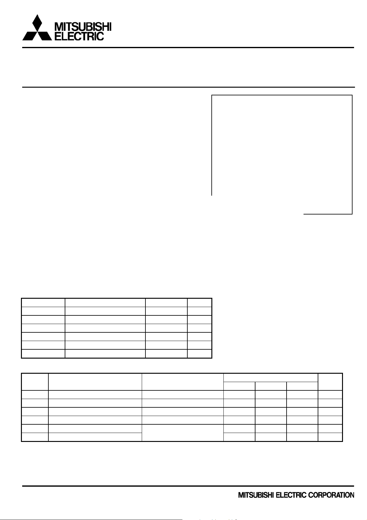
ABSOLUTE MAXIMUM RATINGS
Symbol Parameter Ratings Unit
V
GDO
V
GSO
ID
PT Total power dissipation 50 mW
Tch
T
stg
Gate to drain voltage -3 V
Gate to source voltage -3 V
Drain current 60 mA
Channel temperature 125 C
Storage temperature -55 to +125 C
ELECTRICAL CHARACTERISTICS
Symbol Parameter Test conditions Limits Unit
MIN. TYP. MAX
V
V
NFmin. Minimum noise figure
Note: Gs and NFmin. are tested with sampling inspection.
(BR)GDO
I
I
GS(off)
Gate to drain breakdown voltage
Gate to source leakage current
GSS
Saturated drain current
DSS
Gate to source cut-off voltage
Gs Associated gain
(Ta=25C )
IG=-10A
VGS=-2V,VDS=0V
VGS=0V,VDS=2V
VDS=2V,ID=500A
VDS=2V,
ID=10mA,f=20GHz
(Ta=25C )
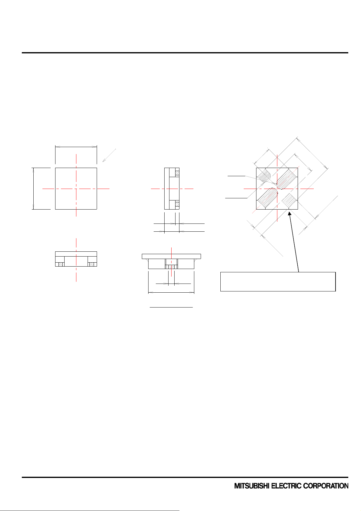
Outline Drawing
Fig.1
-3 -- -- V
-- -- 50 A
15 -- 60 mA
-0.1 -- -1.5 V
9.0 10.5 -- dB
-- 0.55 0.80 dB
Publication Date : Apr., 2011
1
Page 2
< Low Noise GaAs HEMT >
MGF4953B
Leadless ceramic package
Fig.1
Top
+0.20
2.15
-0.10
A
②
①
0
0
2
1
.
.
0
0
+
-
5
1
.
2
J 5
6 E G
②
③
Side
0.20±0.1
0.80±0.1
2-R0.275
2-R0.20
①
②
Bottom
)
2
0
.
1
(
-
2
2
-
0
.
2
-
(
2
②
.
2
0
1
.
)
2
0
±
0
.
0
5
5
0
.
③
5
0
±
0
.
0
5
0
±
5
5
.
0
-
4
(0.30)
(2.30)
from "A" side view
Square shape electrode is Drain
Unit: mm
① Gate
② Source
③ Drain
Publication Date : Apr., 2011
2
Page 3

< Low Noise GaAs HEMT >
)
MGF4953B
Leadless ceramic package
TYPICAL CHARACTERISTICS
50
40
Ta=25
=-0.1V /STEP
V
GS
(mA)
D
I
30
20
Drain Current
10
0
0123
Drain to Sourc e voltage VDS(V)
DRAIN TO SOURCE VOLTAGE VDS (V)
1.3
Ta=25
1.2
1.1
1.0
0.9
NF (dB)
0.8
0.7
雑音指数
0.6
0.5
0.4
=2V
V
DS
f=20GHz
0 5 10 15 20
℃
℃
ID vs. V
DS
NF & G s VS. I
ドレイン電流
ID (mA )
Gs
NF
D
(Ta=25°C)
13
12
11
10
9
8
7
6
5
4
ID VS. V
50
Ta=25
℃
=2V
V
DS
40
(mA)
D
I
30
20
Drain Current
10
0
-1.00 -0.50 0.00
Gate to Source voltage VGS(V)
GATE TO SOURCE VOLTAGE VGS (V)
雑音最小電力利得 Gs (dB)
GS
Publication Date : Apr., 2011
DRAIN CURRENT ID (mA
3
Page 4

< Low Noise GaAs HEMT >
MGF4953B
Leadless ceramic package
S PARAMETERS
Freq.
(GHz) (mag) (ang) (mag) (ang) (mag) (ang) (mag) (ang)
1 0.989 -4.0 5.212 166.6 0.038 82.4 0.689 -10.7
2 0.968 -20.4 5.101 152.0 0.046 72.4 0.669 -21.1
3 0.942 -36.8 4.989 137.3 0.054 62.4 0.640 -31.5
4 0.927 -53.2 4.877 122.7 0.062 52.4 0.604 -41.9
5 0.857 -69.5 4.766 108.0 0.070 42.4 0.554 -52.4
6 0.787 -85.8 4.655 93.4 0.078 32.4 0.505 -62.7
7 0.716 -101.5 4.524 79.3 0.085 23.5 0.454 -72.7
8 0.654 -119.2 4.378 64.9 0.093 13.5 0.399 -84.1
9 0.582 -135.3 4.162 52.0 0.095 4.9 0.341 -93.6
10 0.525 -152.8 4.008 39.5 0.095 -2.5 0.288 -102.8
11 0.494 -170.2 3.887 27.3 0.096 -8.4 0.250 -113.0
12 0.474 171.2 3.761 15.2 0.096 -14.2 0.212 -124.7
13 0.471 152.0 3.656 2.9 0.097 -20.6 0.180 -140.4
14 0.484 134.6 3.593 -9.4 0.096 -26.0 0.159 -156.4
15 0.501 118.4 3.522 -21.9 0.095 -33.2 0.155 -175.5
16 0.544 101.2 3.335 -36.1 0.098 -37.5 0.163 153.3
17 0.579 86.8 3.209 -49.3 0.099 -42.9 0.182 132.4
18 0.612 73.6 3.038 -62.7 0.101 -49.3 0.216 110.1
19 0.646 62.0 2.814 -73.7 0.102 -56.2 0.260 90.7
20 0.688 50.3 2.726 -85.1 0.107 -63.9 0.301 76.3
21 0.733 39.4 2.613 -96.7 0.112 -75.1 0.340 59.0
22 0.765 28.6 2.499 -108.3 0.115 -86.3 0.370 48.0
23 0.798 17.7 2.384 -120.0 0.119 -97.5 0.405 37.0
24 0.831 6.9 2.269 -131.6 0.123 -108.7 0.444 30.2
25 0.831 -3.9 2.152 -143.2 0.127 -119.9 0.483 23.1
26 0.814 -14.7 2.034 -154.8 0.131 -131.1 0.522 17.1
NOISE PARAMETERS
(VDS=2V,ID=10mA, Ta=25C)
S22S11 S21 S12
(VDS=2V, ID=10mA, Ta=25C)
Freq. NFmin Rn
(GHz) (dB) (mag) (ang) (Ω)
12 0.38 0.44 140.9 2.5
13 0.40 0.40 160.3 1.5
14 0.43 0.38 -179.4 2.0
15 0.45 0.36 -158.4 2.0
16 0.48 0.36 -136.6 3.0
17 0.50 0.36 -114.2 4.0
18 0.53 0.38 -91.2 6.0
19 0.57 0.39 -67.9 8.5
20 0.63 0.41 -44.5 11.5
21 0.72 0.45 -21.1 15.0
22 0.80 0.48 2.1 19.0
23 0.92 0.54 25.2 24.0
24 1.00 0.57 48.1 29.5
25 1.14 0.61 70.9 37.5
26 1.24 0.63 93.6 50.0
opt
Measurement plane (2.2mm)
Board; RO4003C (Rogers Corp.)
r=3.38, t=0.508mm, Au (Cu) =0.035mm
Note:
We are ready to provide nonlinear model for ADS and MWO users. If you are interested, please contact our sales
offices.
Publication Date : Apr., 2011
4
Page 5

< Low Noise GaAs HEMT >
MGF4953B
Leadless ceramic package
S PARAMETERS
Freq. S22
(GHz) (mag) (ang) (mag) (ang) (mag) (ang) (mag) (ang)
1 0.989 -13.0 4.537 165.8 0.014 78.9 0.637 -9.7
2 0.973 -25.9 4.502 152.9 0.028 71.8 0.629 -19.6
3 0.949 -38.7 4.472 140.4 0.041 62.7 0.621 -29.2
4 0.926 -52.0 4.460 127.3 0.054 53.2 0.608 -39.0
5 0.890 -64.9 4.431 114.9 0.066 44.4 0.592 -48.2
6 0.828 -81.1 4.394 99.8 0.076 33.4 0.539 -60.1
7 0.776 -95.6 4.311 86.3 0.085 24.1 0.505 -70.2
8 0.723 -110.6 4.230 73.2 0.093 15.2 0.469 -80.4
9 0.662 -126.6 4.094 59.9 0.099 5.4 0.423 -90.7
10 0.605 -142.6 3.943 47.4 0.102 -4.0 0.368 -100.2
11 0.551 -158.2 3.826 35.4 0.102 -12.9 0.318 -108.8
12 0.514 -174.5 3.740 23.7 0.100 -19.7 0.279 -116.3
13 0.488 167.0 3.622 11.2 0.099 -28.1 0.232 -126.2
14 0.486 149.0 3.572 -1.1 0.098 -32.1 0.203 -138.3
15 0.480 131.8 3.512 -12.6 0.094 -38.4 0.169 -148.1
16 0.509 113.0 3.425 -26.2 0.099 -43.0 0.148 -175.1
17 0.536 95.1 3.349 -39.1 0.099 -49.9 0.133 157.1
18 0.569 78.2 3.226 -52.1 0.100 -58.5 0.132 120.7
19 0.609 62.7 3.091 -66.1 0.099 -66.5 0.160 92.2
20 0.642 47.3 2.934 -79.2 0.096 -75.2 0.204 67.8
21 0.674 34.3 2.752 -91.8 0.091 -83.8 0.250 50.6
22 0.707 21.1 2.617 -104.8 0.089 -92.5 0.293 37.0
23 0.742 9.2 2.471 -117.4 0.082 -102.8 0.350 23.8
24 0.753 -2.2 2.307 -130.2 0.081 -111.9 0.390 13.5
25 0.775 -12.5 2.139 -142.4 0.072 -118.9 0.430 2.4
26 0.803 -22.5 2.008 -155.0 0.069 -135.9 0.474 -5.7
(VDS=2V,ID=10mA, Ta=25C)
S11 S21 S12
NOISE PARAMETERS (VDS=2V,ID=10mA, Ta=25C)
opt
Freq. Rn NFmin
(GHz) (mag) (ang) (dB)
18 0.358 -137.2 0.12 0.51
20 0.372 -91.0 0.14 0.55
22 0.390 -47.7 0.63 0.77
24 0.417 -14.9 1.05 1.05
26 0.473 10.5 1.26 1.25
Note) Rn is normalized by 50ohm
Note:
We are ready to provide nonlinear model for ADS and MWO users. If you are interested, please contact our sales
offices.
Board: r=2.6
Thickness=0.4mm
HEMT mount
Gate
4-φ0.4
0.65
Reference Point Reference Point 2.2mm
1.20
Drain
1.0mm
Publication Date : Apr., 2011
5
Page 6

< Low Noise GaAs HEMT >
MGF4953B
Leadless ceramic package
Mitsubishi Electric Corporation puts the maximum effort into making semiconductor products better and
more reliable, but there is always the possibility that trouble may occur with them. Trouble with
semiconductors may lead to personal injury, fire ore property damage. Remember to give due
consideration to safety when making your circuit designs, with appropriate measures such as (i) placement
of substitutive, auxiliary circuits, (ii) use of non-flammable material or (iii) prevention against any
malfunction or mishap.
These materials are intended as a reference to assist our customers in the selection of the Mitsubishi
semiconductor product best suited to the customer’s application; they do not convey any license under any
intellectual property rights, or any other rights, belonging to Mitsubishi Electric Corporation or a third party.
Mitsubishi Electric Corporation assumes no responsibility for any damage, or infringement of any third-
party’s rights, originating in the use of any product data, diagrams, charts, programs, algorithms, or circuit
application examples contained in these materials.
All information contained in these materials, including product data, diagrams, charts, programs and
algorithms represents information on products at the time of publica tion of these materials, an d are subje ct
to change by Mitsubishi Electric Corporation without notice due to prod uct imp rov ements or other reasons.
It is therefore recommended that customers contact Mitsubishi Electric Corporation or an authorized
Mitsubishi Semiconductor product distri butor for the l atest product informatio n before purchasing a prod uct
listed herein.
The information described here may contain technical in accuracies or typographi cal errors.
Mitsubishi Electric Corporation assumes no responsibility for any damage, liability, or other loss rising from
these inaccuracies or errors.
Please also pay attention to information published by Mitsubishi Electric Corporation by various means,
including the Mitsubishi Semiconductor home page (http://www.mitsubishielectric.com/).
When using any or all of the information contained in these materials, including product data, diagrams,
charts, programs, and algorithms, please be sure to evaluate all information as a total system before
making a final decision on the applicability of the information and products. Mitsubishi Electric Corporation
assumes no responsibility for any damage, liability or other loss resulting from the information contained
herein.
Mitsubishi Electric Corporation semiconductors are not designed or manufactured for use in a device or
system that is used under circumstances in which human life is potentially at stake. Please contact
Mitsubishi Electric Corporation or an authorized Mitsubishi Semiconductor product distributor when
considering the use of a product contained herein fo r any specific purposes, such as apparatus or systems
for transportation, vehicular, medical, aerospace, nuclear, or undersea repeater use.
The prior written approval of Mitsubishi Electric Corporation is necessary to reprint or reproduce in whole
ore in part these materials.
If these products or technologies are subject to the Japanese export control restrictions, they must be
exported under a license from the Japanese government and cannot be imported into a country other than
the approved destination.
Any diversion or re-export contrary to the export control laws and regulations of Japan and/or the country
of destination is prohibited.
Please contact Mitsubishi Electric Corporation or an authorized Mitsubishi Semiconductor product
distributor for further details on these materials or the products contained therein.
© 2011 MITSUBISHI ELECTRIC CORPORATION. ALL RIGHTS RESERVED.
Keep safety first in your circuit designs!
Notes regarding these materials
Publication Date : Apr., 2011
6
 Loading...