

Page 1
June/2004
MITSUBISHI SEMICONDUCTOR <GaAs FET>
MGF4951A/MGF4952A
SUPER LOW NOISE InGaAs HEMT (Leadless Ceramic Package)
DESCRIPTION
The MGF4951A/MGF4952A super-low noise HEMT (High
Electron Mobility Transistor) is designed for use in C to K band
amplifiers.
The lead-less ceramic package assures minimum parasitic losses.
FEATURES
Low noise figure @ f=12GHz
MGF4951A : NFmin. = 0.40dB (Typ.)
MGF4952A : NFmin. = 0.60dB (Typ.)
High associated gain @ f=12GHz
Gs = 12.0dB (Typ.)
APPLICATION
C to K band low noise amplifiers
MITSUBISHI Proprietary
Not to be reproduced or disclosed
without permission by Mitsubishi Electric
QUALITY GRADE
GG
RECOMMENDED BIAS CONDITIONS
VDS=2V , ID=10mA
ORDERING INFORMATION
Tape & reel 3000pcs./reel
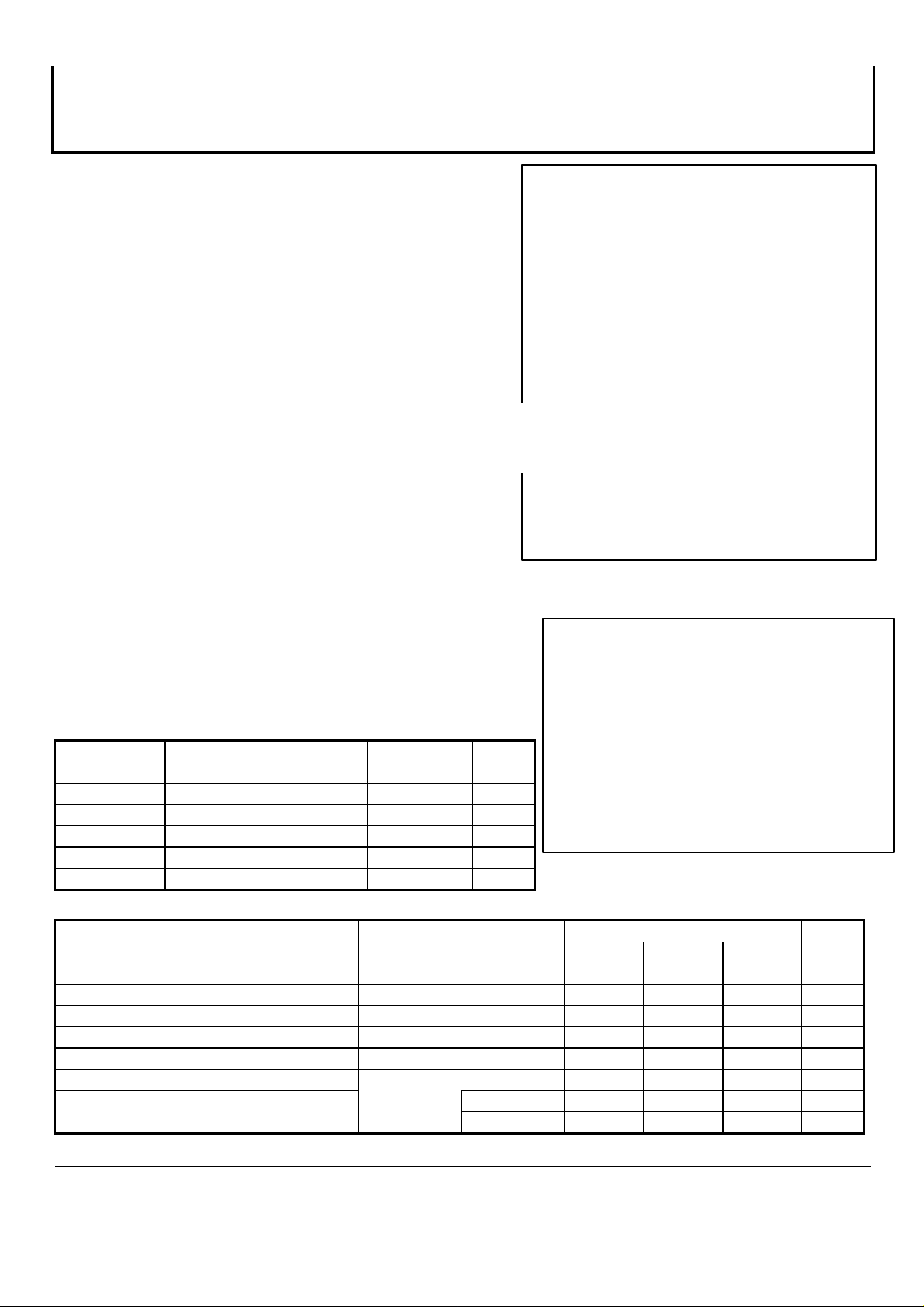
ABSOLUTE MAXIMUM RATINGS
Symbol Parameter Ratings Unit
V
GDO
V
GSO
ID
PT Total power dissipation 50 mW
Tch
T
stg
Gate to drain voltage -4 V
Gate to source voltage -4 V
Drain current 60 mA
Channel temperature 125 °C
Storage temperature -65 to +125 °C
(Ta=25°C )
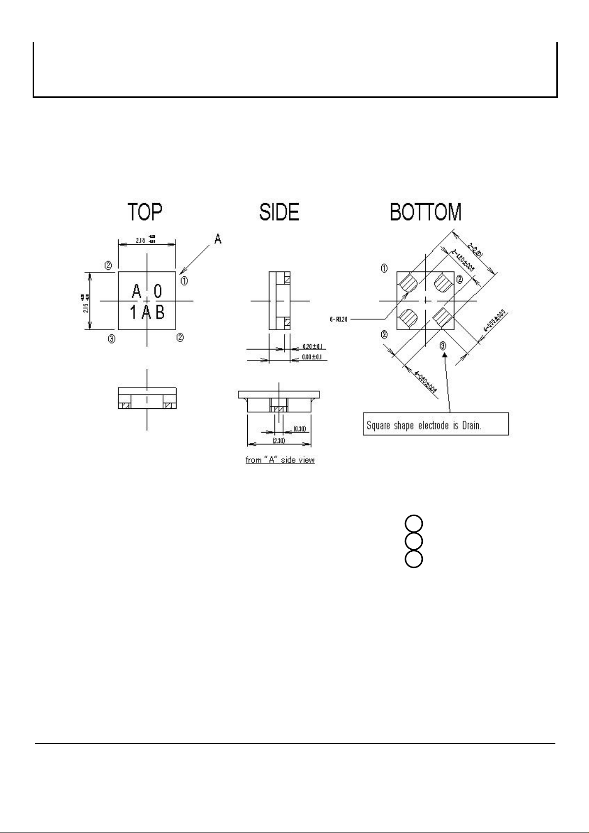
Outline Drawing
Fig.1
Keep Safety first in your circuit designs!
Mitsubishi Electric Corporation puts the maximum
effort into making semiconductor products better
and more reliable , but there is always the
possibility that trouble may occur with them.
Trouble with semiconductors may lead to personal
injury , fire or property damage. Remember to give
due consideration to safety when making your
circuit designs , with appropriate measure such
as (I) placement of substitutive , auxiliary circuits ,
(ii) use of non-flammable material or (iii) prevention
against any malfunction or mishap.
ELECTRICAL CHARACTERISTICS
Synbol Parameter Test conditions Limits Unit
MIN. TYP. MAX
V
(BR)GDO
V
NFmin.
I
GSS
I
DSS
GS(off)
gm
Gs
Gate to drain breakdown voltage
Gate to source leakage current
Saturated drain current
Gate to source cut-off voltage
Transconductance
Associated gain
Minimum noise figure
(Ta=25°C )
IG=-10µA
VGS=-2V,VDS=0V
VGS=0V,VDS=2V
VDS=2V,ID=500µA
VDS=2V,ID=10mA
VDS=2V,
ID=10mA
f=12GHz
-3 -- -- V
-- -- 50 µA
15 -- 60 mA
-0.1 -- -1.5 V
-- 70 -- mS
11.0 12.0 -- dB
MGF4951A
MGF4952A
-- 0.40 0.50 dB
-- 0.60 0.80 dB
MITSUBISHI
(1/5)
June/2004
Page 2
June/2004
MITSUBISHI SEMICONDUCTOR <GaAs FET>
MGF4951A/MGF4952A
SUPER LOW NOISE InGaAs HEMT (Leadless Ceramic Package)
Fig.1
Unit : mm
1 Gate
2 Source
3 Drain
MITSUBISHI
(2/5)
June/2004
Page 3
June/2004
MITSUBISHI SEMICONDUCTOR <GaAs FET>
MGF4951A/MGF4952A
SUPER LOW NOISE InGaAs HEMT (Leadless Ceramic Package)
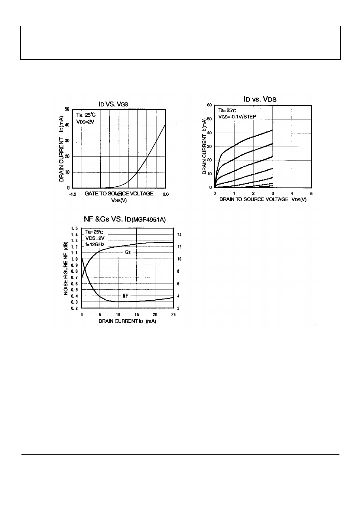
TYPICAL CHARACTERISTICS
(Ta=25°C)
MITSUBISHI
(3/5)
June/2004
Page 4
June/2004
MITSUBISHI SEMICONDUCTOR <GaAs FET>
MGF4951A/MGF4952A
SUPER LOW NOISE InGaAs HEMT (Leadless Ceramic Package)
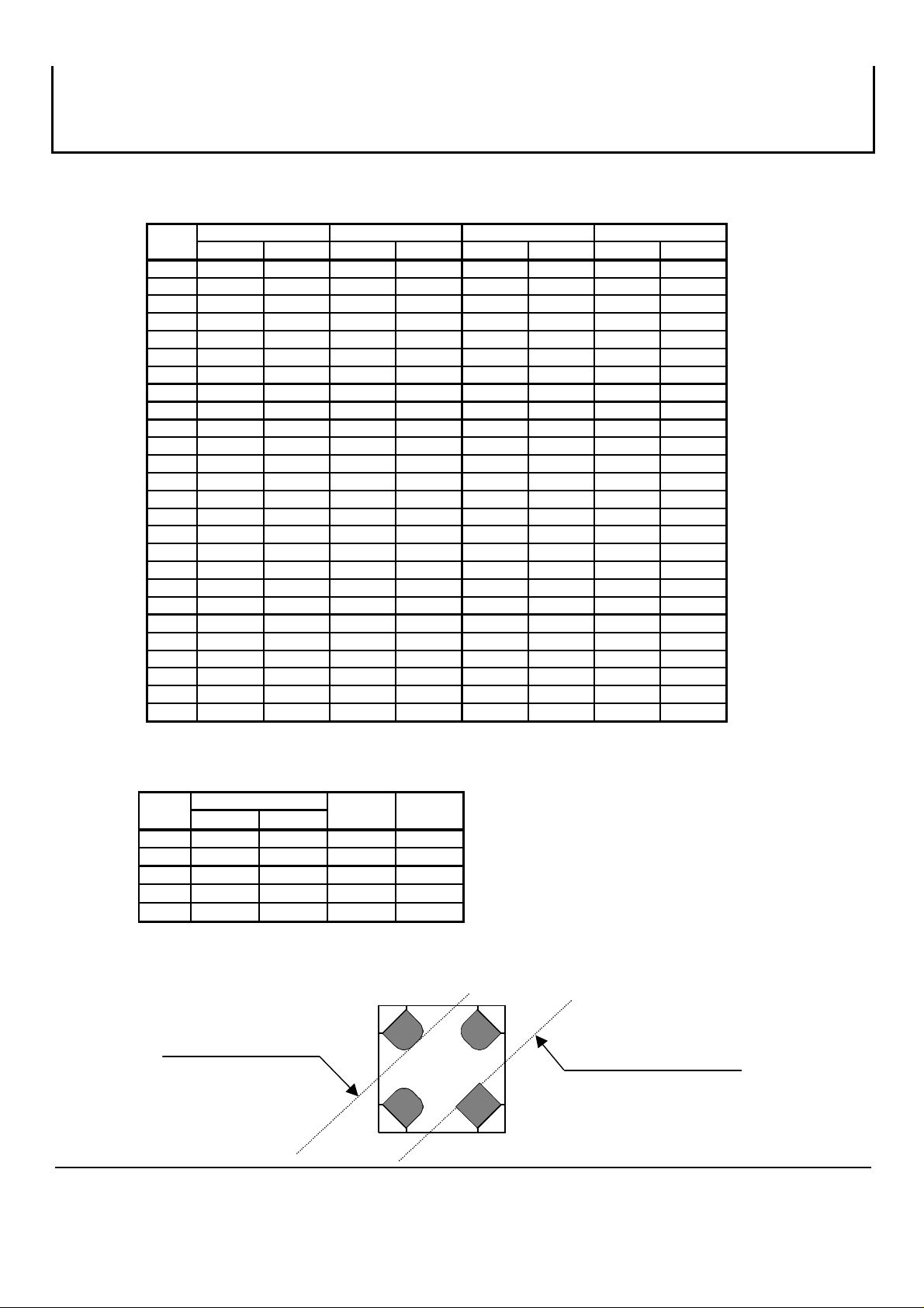
S PARAMETERS
f S11 S21 S12 S22
(GHz) Magn. Angle Magn. Angle Magn. Angle Magn. Angle
1.0 0.978 -14.5 4.800 163.6 0.019 78.3 0.525 -13.5
2.0 0.930 -26.3 4.857 152.8 0.037 72.5 0.513 -22.5
3.0 0.884 -43.8 4.702 133.4 0.053 59.5 0.491 -37.6
4.0 0.818 -59.6 4.514 119.5 0.066 51.1 0.458 -47.5
5.0 0.768 -71.1 4.224 108.2 0.076 44.7 0.449 -54.6
6.0 0.722 -80.2 4.008 98.9 0.084 40.1 0.444 -58.7
7.0 0.681 -88.9 3.841 89.8 0.092 36.6 0.439 -61.2
8.0 0.652 -100.4 3.681 45.6 0.099 27.8 0.440 -68.2
9.0 0.627 -17.3 3.540 66.6 0.108 24.0 0.444 -70.2
10.0 0.593 -114.4 3.476 57.5 0.117 21.3 0.442 -72.3
11.0 0.542 -123.2 3.474 47.7 0.130 15.6 0.418 -76.0
12.0 0.475 -133.8 3.487 37.0 0.142 9.6 0.380 -78.3
13.0 0.406 -148.6 3.458 25.5 0.153 2.4 0.326 -82.4
14.0 0.333 -178.7 3.415 7.5 0.162 -11.0 0.234 -90.5
15.0 0.298 147.3 3.309 -5.6 0.172 -20.2 0.132 -83.7
16.0 0.338 110.1 3.150 -20.1 0.175 -30.0 0.068 -20.3
17.0 0.443 81.5 2.965 -34.2 0.176 -39.6 0.169 25.0
18.0 0.564 60.0 2.670 -48.8 0.171 -50.4 0.301 26.1
19.0 0.675 44.4 2.323 -62.6 0.159 -60.0 0.431 21.3
20.0 0.763 32.1 2.030 -74.2 0.146 -69.4 0.537 15.7
21.0 0.846 18.5 1.714 -90.8 0.133 -80.3 0.612 4.5
22.0 0.892 8.8 1.457 -101.1 0.119 -86.8 0.684 1.2
23.0 0.912 1.4 1.233 -109.9 0.104 -92.2 0.749 -2.5
24.0 0.927 -4.8 1.026 -118.4 0.093 -95.3 0.796 -5.5
25.0 0.932 -9.4 0.864 -124.7 0.080 -98.0 0.843 -7.1
26.0 0.933 -14.0 0.732 -130.2 0.069 -100.6 0.881 -8.6
(Ta=25°C,VDS=2V,ID=10mA)
NOISE PARAMETERS
f Ganma-opt Rn NF
(GHz) Magn. Angle (ohm) (dB)
4.0 0.64 49.7 0.21 0.21
8.0 0.61 100.5 0.12 0.31
12.0 0.55 143.4 0.04 0.45
14.0 0.51 158.9 0.03 0.52
18.0 0.41 172.5 0.06 0.66
Note) Rn is normalized by 50-ohm
Reference Point
(Ta=25°C,VDS=2V,ID=10mA)
Gate
Source
Source
Reference Point
Drain
MITSUBISHI
(4/5)
June/2004
Page 5

June/2004
MITSUBISHI SEMICONDUCTOR <GaAs FET>
MGF4951A/MGF4952A
SUPER LOW NOISE InGaAs HEMT (Leadless Ceramic Package)
Requests Regarding Safety Designs
Mitsubishi Electric constantly strives to raise the level of its quality and reliability. Despite these concerted efforts,
however, there will be occasions when our semiconductor products suffer breakdowns, malfunctions or other problems.
In view of this reality, it is requested that every feasible precaution be taken in the pursuit of redundancy design,
malfunction prevention design and other safety- related designs, to prevent breakdowns or malfunctions in our products
from resulting in accidents involving people, fires, social losses or other problems, thereby upholding the highest levels of
safety in the products when in use by customers.
Matters of Importance when Using these Materials
1. These materials are designed as reference materials to ensure that all customers purchase Mitsubishi Electric
semiconductors best suited to their specific use applications. Please be aware, however, that the technical information
contained in these materials does not comprise consent for the execution or use of intellectual property rights or other
rights owned by Mitsubishi Electric Corporation.
2. Mitsubishi Electric does not assume responsibility for damages resulting from the use of product data, graphs, charts,
programs, algorithms or other applied circuit examples described in these materials, or for the infringement of the
rights of third-party owners resulting from such use.
3. The data, graphs, charts, programs, algorithms and all other information described in these materials were current at
the issue of these materials, with Mitsubishi Electric reserving the right to make any necessary updates or changes in
the products or specifications in these materials without prior notice. Before purchasing Mitsubishi Electric
semiconductor products, therefore, please obtain the latest available information from Mitsubishi Electric directly or an
authorized dealer.
4. Every possible effort has been made to ensure that the information described in these materials is fully accurate.
However, Mitsubishi Electric assumes no responsibility for damages resulting from inaccuracies occurring within these
materials.
5. When using the product data, technical contents indicated on the graphs, charts, programs or algorithms described in
these materials, assessments should not be limited to only the technical contents, programs and algorithm units.
Rather, it is requested that ample evaluations be made of each individual system as a whole, with the customer
assuming full responsibility for decisions on the propriety of application. Mitsubishi Electric does not accept
responsibility for the propriety of application.
6. The products described in these materials, with the exception of special mention concerning use and reliability, have
been designed and manufactured with the purpose of use in general electronic machinery. Accordingly these products
have not been designed and manufactured with the purpose of application in machinery or systems that will be used
under conditions that can affect human life, or in machinery or systems used in social infrastructure that demand a
particularly high degree of reliability. When considering the use of the products described in these materials in
transportation machinery (automobiles, trains, vessels), for objectives related to medical treatment, aerospace, nuclear
power control, submarine repeaters or systems or other specialized applications, please consult with Mitsubishi Electric
directly or an authorized dealer.
7. When considering use of products for purposes other than the specific applications described in these materials,
please inquire at Mitsubishi Electric or an authorized dealer.
8. The prior consent of Mitsubishi Electric in writing is required for any reprinting or reproduction of these materials.
9. Please direct any inquiries regarding further details of these materials, or any other comments or matters of attention,
to Mitsubishi Electric or an authorized dealer.
MITSUBISHI
(5/5)
June/2004
 Loading...