

Page 1
MITSUBISHI Proprietary
< Low Noise GaAs HEMT >
MGF4941AL
Micro-X type plastic package
DESCRIPTION
The MGF4941AL super-low noise InGaAs HEMT (High Electron Mobility
Transistor) is designed for use in Ku band amplifiers.
FEATURES
Low noise figure @ f=12GHz
NFmin. = 0.35dB (Typ.)
High associated gain @ f=12GHz
Gs = 13.5dB (Typ.)
APPLICATION
L to K band low noise amplifiers
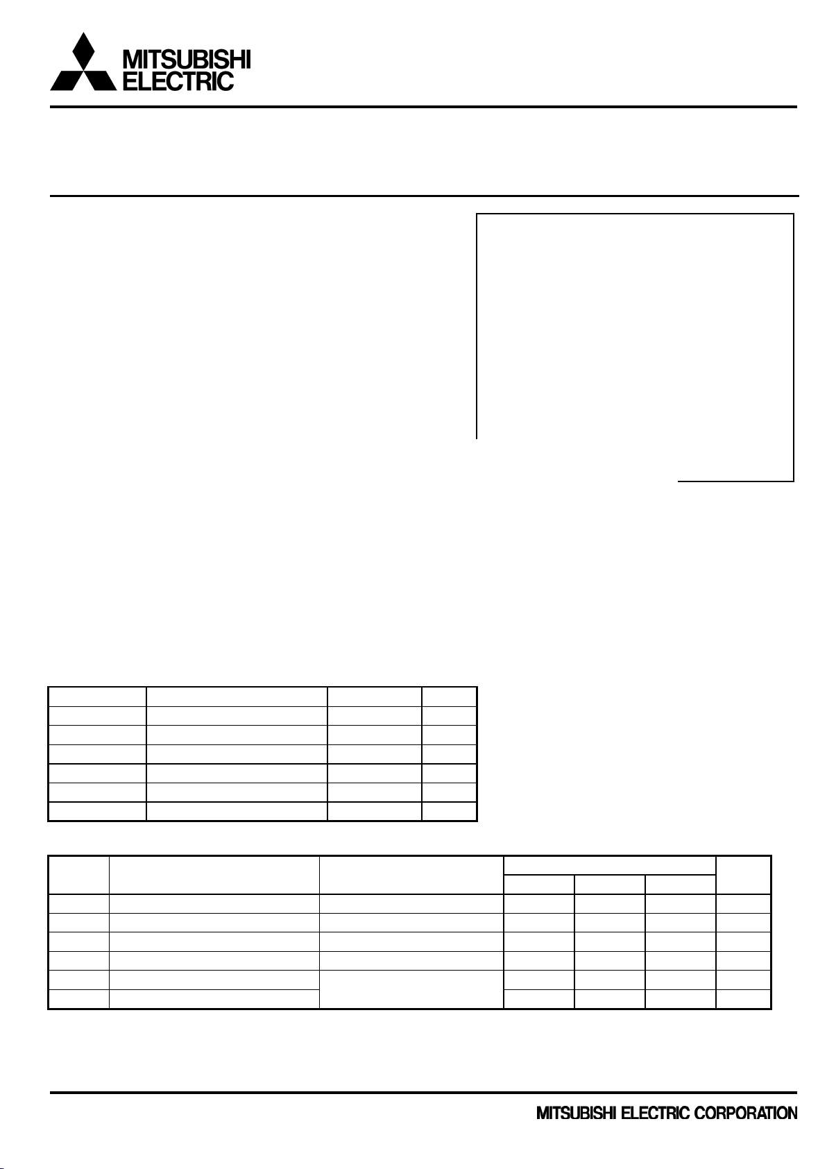
Outline Drawing
Fig.1
QUALITY GRADE
GG
RECOMMENDED BIAS CONDITIONS
=2V, ID=10mA
V
DS
ORDERRING INFORMATION
Tape & reel 4000pcs./reel
Not to be reproduced or disclosed without
permission by Mitsubishi Electric
RoHS COMPLIANT
MGF4941AL is a RoHS compliant product. RoHS compliance is indicated by the letter “G” after the Lot Marking.
ABSOLUTE MAXIMUM RATINGS
Symbol Parameter Ratings Unit
V
GDO
V
GSO
ID
PT Total power dissipation 50 mW
Tch
T
stg
Gate to drain voltage -3 V
Gate to source voltage -3 V
Drain current IDSS mA
Channel temperature 125 °C
Storage temperature -55 to +125 °C
(Ta=25°C )
ELECTRICAL CHARACTERISTICS
Symbol
V
(BR)GDO
I
I
V
GS(off)
NFmin. Minimum noise figure
Note: Gs and NFmin. are tested with sampling inspection.
Gate to drain breakdown voltage
Gate to source leakage current
GSS
Saturated drain current
DSS
Gate to source cut-off voltage
Gs Associated gain
Parameter Test conditions
IG=-10µA
VGS=-2V,VDS=0V
VGS=0V,VDS=2V
VDS=2V,ID=500µA
VDS=2V,
ID=10mA,f=12GHz
(Ta=25°C )
Limits Unit
MIN. TYP. MAX
-3 -- -- V
-- -- 50 µA
15 -- 60 mA
-0.1 -- -1.5 V
12.0 13.5 -- dB
-- 0.35 0.5 dB
Publication Date : Apr., 2011
1
Page 2
<Low Noise GaAs HEMT>
A
MGF4941AL
Micro-X type plastic package
Fig.1
①
3.2±0.1
2.6±0.1(0.30)
0.5±0.1
(0.30)
Bottom
(2.3)
(0.30)
Top
②
rAA
②
0.65±0.1
3.2±0.1
2.6±0.1
(2.3)
(0.30)
③
2.2±0.1
1.7±0.1
Unit : mm
Side
0.15±0.05
1.35±0.2
① Gate
② Source
③ Drain
(GD-32)
Publication Date : Apr., 2011
2
Page 3
<Low Noise GaAs HEMT>
V
V
MGF4941AL
Micro-X type plastic package
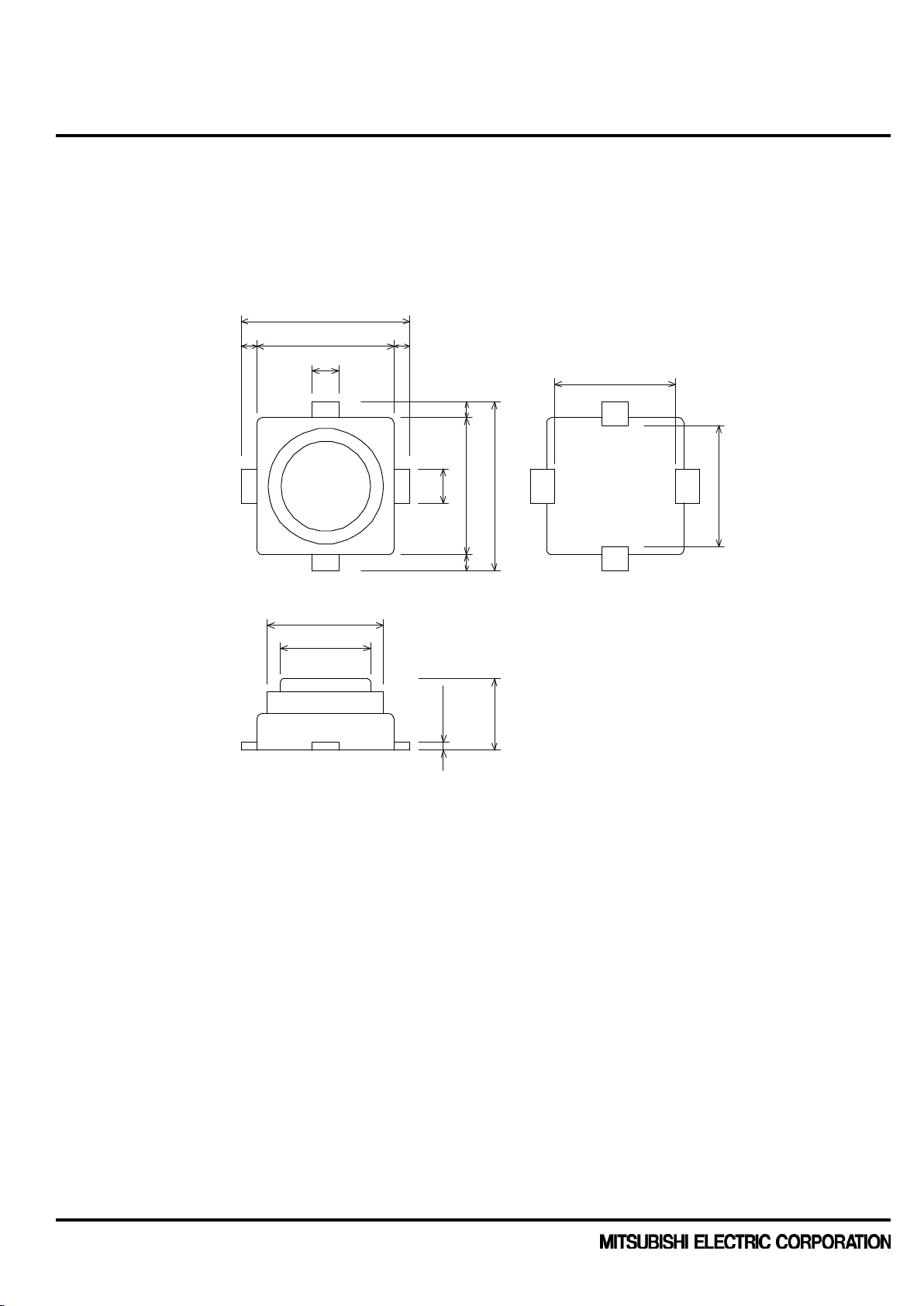
TYPICAL CHARACTERISTICS
Ta=25°C)
(
50
40
(mA )
D
I
30
20
=-0.1V /STEP
GS
ID vs. V
DS
ID vs. V
50
VDS=2V
40
(mA)
D
30
20
GS
10
DRAIN CURRENT
0
0 1 2 3
Drain to Sourc e voltage VDS(V)
1.2
1.0
=2V
DS
f=12GHz
NF & Gs vs. I
D
16
14
Gs
10
DRAIN CURRENT, I
0
-1.0 -0.5 0.0
Gate to Source voltage, VGS(V)
0.8
12
0.6
10
0.4
NOISE FIGURE, NF (dB )
NF
8
ASSOCIAT ED GAIN, Gs (dB)
0.2
0 5 10 15 20
DRAIN CURRE NT, ID (m A )
6
Publication Date : Apr., 2011
3
Page 4

<Low Noise GaAs HEMT>
(GHz)
(mag)
(ang)
(mag)
(ang)
(mag)
(ang)
(mag)
(ang)
18
0.643
73.3
2.620
-65.9
0.153
-26.4
0.317
106.1
Freq.
NFmin
Rn
(GHz)
(dB)
(mag)
(ang)
(Ω)
18
0.72
0.66
-47.0
8.7
Γ
MGF4941AL
Micro-X type plastic package
S PARAMETERS
Freq.
1 0.997 -18.3 5.603 158.4 0.023 73.4 0.702 -11.1
2 0.976 -30.0 5.399 145.6 0.033 67.2 0.668 -20.1
3 0.944 -41.7 5.195 132.7 0.043 61.0 0.634 -29.1
4 0.880 -53.4 4.991 119.8 0.053 54.8 0.600 -38.1
5 0.804 -67.6 4.874 105.3 0.064 46.8 0.563 -47.6
6 0.728 -82.3 4.743 90.7 0.074 39.0 0.519 -57.2
7 0.640 -98.0 4.569 76.0 0.082 31.0 0.467 -66.6
8 0.563 -116.4 4.389 61.2 0.091 22.3 0.406 -77.4
9 0.476 -134.2 4.123 47.5 0.095 15.2 0.343 -86.1
10 0.408 -153.5 3.898 34.7 0.095 9.9 0.285 -94.4
11 0.381 -174.5 3.736 22.2 0.101 5.8 0.245 -105.3
12 0.370 163.2 3.559 9.8 0.105 1.9 0.203 -119.0
13 0.385 141.3 3.391 -2.6 0.110 -3.1 0.167 -137.9
14 0.415 124.1 3.275 -14.2 0.113 -5.8 0.156 -157.0
15 0.458 109.1 3.148 -26.2 0.117 -10.7 0.153 178.7
16 0.529 94.8 2.961 -40.7 0.131 -15.1 0.214 144.7
17 0.586 83.3 2.817 -53.4 0.142 -19.9 0.257 125.9
Noise Parameter
Note
1 0.18 0.96 -32.8 17.0
2 0.19 0.93 -17.9 15.5
3 0.19 0.90 -3.0 14.0
4 0.20 0.84 11.9 12.5
5 0.23 0.79 26.8 11.0
6 0.24 0.74 41.7 9.5
7 0.26 0.65 56.6 8.0
8 0.29 0.53 73.6 6.0
9 0.31 0.44 92.6 4.5
10 0.34 0.34 113.6 3.5
11 0.37 0.28 136.5 2.5
12 0.40 0.25 161.2 2.5
13 0.45 0.25 -172.3 2.5
14 0.50 0.27 -144.2 3.0
15 0.55 0.33 -122.0 4.0
16 0.61 0.44 -97.0 5.6
17 0.66 0.55 -73.0 7.0
:
We are ready to provide nonlinear model for ADS and MWO users. If you are interested, please contact our sales
(VDS=2V,ID=10mA,Ta=room temperature)
(VDS=2V,ID=10mA, Ta=room temperature)
opt
S22S11 S21 S12
Measurement plane (2.6mm)
Recommended foot pattern;
RO4003C/Rogers (εr=3.38, t=0.508mm)
offices.
Publication Date : Apr., 2011
4
Page 5

<Low Noise GaAs HEMT>
Freq.
rn
NFmin
(GHz)
(mag)
(ang)
(dB)
22
0.467
-42.7
0.180
0.96
Γ
opt
MGF4941AL
Micro-X type plastic package
S PARAMETERS
(VDS=2V,ID=10mA,Ta=room temperature)
Freq. S22
(GHz) (mag) (ang) (mag) (ang) (mag) (ang) (mag) (ang)
1 0.989 -13.9 5.497 164.6 0.017 78.9 0.637 -10.6
2 0.967 -28.2 5.416 149.6 0.028 70.9 0.626 -21.1
3 0.929 -41.5 5.278 135.0 0.040 61.7 0.610 -31.1
4 0.882 -54.4 5.172 121.5 0.051 53.3 0.586 -40.5
5 0.822 -65.9 4.932 108.0 0.061 45.9 0.572 -50.8
6 0.757 -79.5 4.959 94.1 0.071 37.6 0.538 -60.3
7 0.686 -93.3 4.826 80.4 0.080 29.9 0.502 -69.8
8 0.611 -108.8 4.732 66.8 0.086 22.7 0.456 -78.6
9 0.533 -125.1 4.587 53.6 0.092 16.2 0.408 -86.5
10 0.463 -143.6 4.403 40.5 0.096 10.2 0.359 -93.8
11 0.411 -164.1 4.140 27.8 0.100 4.8 0.311 -100.7
12 0.382 174.7 4.010 15.6 0.105 0.1 0.267 -108.9
13 0.378 152.3 3.782 3.3 0.111 -4.7 0.221 -119.3
14 0.395 131.4 3.653 -9.1 0.115 -9.7 0.182 -135.4
15 0.435 113.6 3.514 -21.3 0.121 -14.6 0.152 -157.0
16 0.486 99.0 3.366 -32.9 0.126 -19.8 0.134 177.7
17 0.543 86.2 3.172 -45.3 0.133 -25.5 0.139 145.4
18 0.603 73.7 3.049 -57.7 0.140 -31.2 0.183 115.8
19 0.663 61.2 2.877 -70.2 0.147 -37.9 0.251 95.1
20 0.704 50.1 2.641 -81.3 0.152 -45.0 0.309 80.2
21 0.746 40.5 2.470 -91.5 0.156 -52.4 0.363 70.0
22 0.778 32.3 2.311 -102.3 0.156 -58.0 0.411 59.8
S11 S21 S12
NOISE PARAMETERS
2 0.671 13.9 0.370 0.20
4 0.598 37.2 0.262 0.22
6 0.537 60.8 0.197 0.25
8 0.474 86.2 0.155 0.29
10 0.399 119.2 0.102 0.32
12 0.329 147.6 0.062 0.35
14 0.299 173.6 0.069 0.40
16 0.349 -143.9 0.083 0.49
18 0.392 -106.5 0.109 0.59
20 0.432 -73.0 0.146 0.73
Note: rn is normarised by 50 ohm.
(VDS=2V,ID=10mA, Ta=25°C)
Board: εr=2.2
Thickness: 0.25mm
(4-φ0.3: through-hole)
Reference
(Unit: mm)
2.60
Reference
0.74
(1.0mm)
1.30
Note
:
We are ready to provide nonlinear model for ADS and MWO users. If you are interested, please contact our sales
offices.
2.08
Publication Date : Apr., 2011
5
Page 6

<Low Noise GaAs HEMT>
our sales offices.
MGF4941AL
Micro-X type plastic package
S PARAMETERS
(VDS=0V,VGS=0V,Ta=room temperature)
(V
Freq. S22
(GHz) (mag) (ang) (mag) (ang) (mag) (ang) (mag) (ang)
1 0.996 -12.6 0.008 90.7 0.008 93.1 0.700 167.0
2 0.998 -25.4 0.019 92.4 0.019 92.2 0.696 154.5
3 0.988 -38.1 0.032 90.0 0.032 90.6 0.703 142.2
4 0.984 -50.8 0.048 86.4 0.048 86.3 0.708 129.1
5 0.971 -62.6 0.068 80.5 0.069 81.0 0.710 117.1
6 0.963 -77.1 0.092 72.6 0.092 72.7 0.718 104.8
7 0.949 -92.8 0.119 62.9 0.120 62.9 0.730 92.6
8 0.936 -110.9 0.149 51.8 0.150 52.2 0.739 81.3
9 0.915 -131.2 0.181 39.2 0.182 39.5 0.750 70.7
10 0.892 -153.9 0.211 25.5 0.211 25.9 0.760 60.8
11 0.878 -178.2 0.235 10.8 0.237 11.1 0.769 51.6
12 0.870 157.5 0.252 -3.9 0.252 -3.9 0.785 42.8
13 0.868 133.9 0.258 -18.6 0.259 -18.6 0.795 34.7
14 0.875 113.0 0.257 -32.0 0.257 -32.0 0.805 26.9
15 0.883 94.9 0.250 -44.4 0.249 -44.1 0.815 19.2
16 0.895 79.7 0.238 -55.0 0.238 -54.9 0.824 11.6
17 0.901 66.6 0.225 -64.2 0.225 -64.0 0.833 5.2
18 0.912 54.7 0.213 -72.0 0.215 -71.8 0.845 0.1
19 0.923 43.8 0.205 -78.8 0.205 -78.7 0.856 -3.7
20 0.934 34.0 0.201 -85.1 0.202 -85.5 0.861 -8.4
21 0.947 25.0 0.195 -92.1 0.193 -92.7 0.859 -13.1
22 0.945 17.6 0.188 -98.3 0.188 -98.5 0.854 -18.2
DS
=0V,VGS=-2.5V,Ta=room temperature)
Freq. S22
(GHz) (mag) (ang) (mag) (ang) (mag) (ang) (mag) (ang)
1 1.003 -8.2 0.022 80.5 0.023 79.5 0.998 -9.2
2 0.998 -16.7 0.045 72.1 0.045 71.9 0.990 -18.6
3 0.994 -24.6 0.067 62.9 0.067 63.2 0.995 -27.7
4 0.991 -32.2 0.088 54.8 0.089 54.7 0.993 -36.7
5 0.986 -38.9 0.109 46.3 0.110 46.5 0.993 -46.8
6 0.983 -46.7 0.133 37.4 0.132 37.5 0.985 -56.3
7 0.977 -54.4 0.157 28.6 0.158 28.7 0.982 -65.6
8 0.972 -63.3 0.183 18.8 0.184 18.6 0.970 -75.4
9 0.963 -72.7 0.211 8.3 0.210 8.5 0.962 -85.2
10 0.950 -83.2 0.237 -2.6 0.238 -2.7 0.956 -95.5
11 0.938 -94.7 0.263 -14.9 0.264 -14.8 0.945 -106.4
12 0.929 -107.7 0.289 -27.8 0.289 -27.8 0.932 -118.6
13 0.916 -121.9 0.310 -42.3 0.312 -42.2 0.921 -132.8
14 0.911 -137.5 0.326 -58.6 0.327 -58.7 0.914 -149.6
15 0.904 -155.7 0.324 -76.7 0.325 -76.6 0.909 -167.8
16 0.903 -175.3 0.305 -95.2 0.306 -95.4 0.911 173.5
17 0.910 163.6 0.269 -114.1 0.271 -114.4 0.916 153.5
18 0.914 142.1 0.219 -131.5 0.220 -131.6 0.924 133.0
19 0.912 121.4 0.172 -145.0 0.172 -144.9 0.926 114.9
20 0.927 103.4 0.136 -160.1 0.136 -160.2 0.939 99.3
21 0.955 87.0 0.089 -178.2 0.090 -176.6 0.961 84.2
22 0.971 72.1 0.048 167.9 0.049 171.4 0.968 69.8
S11 S21 S12
S11 S21 S12
Note: We are ready to provide nonlinear model for ADS and MWO users. If you are interested, please contact
Publication Date : Apr., 2011
6
Page 7

<Low Noise GaAs HEMT>
MGF4941AL
Micro-X type plastic package
•
Mitsubishi Electric Corporation puts the maximum effort into making semiconductor products better and
more reliable, but there is always the possibility that trouble may occur with them. Trouble with
semiconductors may lead to personal injury, fire ore property damage. Remember to give due
consideration to safety when making your circuit designs, with appropriate measures such as (i) placement
of substitutive, auxiliary circuits, (ii) use of non-flammable material or (iii) prevention against any
malfunction or mishap.
•
These materials are intended as a reference to assist our customers in the selection of the Mitsubishi
semiconductor product best suited to the customer’s application; they do not convey any license under any
intellectual property rights, or any other rights, belonging to Mitsubishi Electric Corporation or a third party.
•
Mitsubishi Electric Corporation assumes no responsibility for any damage, or infringement of any third-
party’s rights, originating in the use of any product data, diagrams, charts, programs, algorithms, or circuit
application examples contained in these materials.
•
All information contained in these materials, including product data, diagrams, charts, programs and
algorithms represents information on products at the time of publication of these materials, and are subject
to change by Mitsubishi Electric Corporation without notice due to product improvements or other reasons.
It is therefore recommended that customers contact Mitsubishi Electric Corporation or an authorized
Mitsubishi Semiconductor product distributor for the latest product information before purchasing a product
listed herein.
The information described here may contain technical in accuracies or typographical errors.
Mitsubishi Electric Corporation assumes no responsibility for any damage, liability, or other loss rising from
these inaccuracies or errors.
Please also pay attention to information published by Mitsubishi Electric Corporation by various means,
including the Mitsubishi Semiconductor home page (http://www.mitsubishielectric.com/).
•
When using any or all of the information contained in these materials, including product data, diagrams,
charts, programs, and algorithms, please be sure to evaluate all information as a total system before
making a final decision on the applicability of the information and products. Mitsubishi Electric Corporation
assumes no responsibility for any damage, liability or other loss resulting from the information contained
herein.
•
Mitsubishi Electric Corporation semiconductors are not designed or manufactured for use in a device or
system that is used under circumstances in which human life is potentially at stake. Please contact
Mitsubishi Electric Corporation or an authorized Mitsubishi Semiconductor product distributor when
considering the use of a product contained herein for any specific purposes, such as apparatus or systems
for transportation, vehicular, medical, aerospace, nuclear, or undersea repeater use.
•
The prior written approval of Mitsubishi Electric Corporation is necessary to reprint or reproduce in whole
ore in part these materials.
•
If these products or technologies are subject to the Japanese export control restrictions, they must be
exported under a license from the Japanese government and cannot be imported into a country other than
the approved destination.
Any diversion or re-export contrary to the export control laws and regulations of Japan and/or the country
of destination is prohibited.
•
Please contact Mitsubishi Electric Corporation or an authorized Mitsubishi Semiconductor product
distributor for further details on these materials or the products contained therein.
© 2011 MITSUBISHI ELECTRIC CORPORATION. ALL RIGHTS RESERVED.
Keep safety first in your circuit designs!
Notes regarding these materials
Publication Date : Apr., 2011
7
 Loading...