

Page 1
MITSUBISHI Proprietary
< Low Noise GaAs HEMT >
MGF4935AM
4pin flat lead package
DESCRIPTION
The MGF4935AM super-low noise InGaAs HEMT (High Electron Mobility
Transistor) is designed for use in S to Ku band amplifiers.
The 4pin flat lead package is small-thin size, and offers high cost
performance.
FEATURES
Low noise figure @ f=12GHz
NFmin. = 0.45dB (Typ.)
High associated gain @ f=12GHz
Gs = 12.0dB (Typ.)
APPLICATION
S to Ku band low noise amplifiers
QUALITY GRADE
GG
RECOMMENDED BIAS CONDITIONS
VDS=2V , ID=10mA
Not to be reproduced or disclosed without
permission by Mitsubishi Electric
ORDERING INFORMATION
Tape & reel 15000pcs/reel
RoHS COMPLIANT
MGF4935AM is a RoHS compliant product. RoHS compliance is indicated by the letter “G” after the Lot Marking.
ABSOLUTE MAXIMUM RATINGS
Symbol Parameter Ratings Unit
V
GDO
V
GSO
ID
PT Total power dissipation 50 mW
Tch
T
stg
Gate to drain voltage -3 V
Gate to source voltage -3 V
Drain current IDSS mA
Channel temperature 125 °C
Storage temperature -55 to +125 °C
(Ta=25°C )
ELECTRICAL CHARACTERISTICS
Symbol
V
(BR)GDO
I
I
V
GS(off)
NFmin. Minimum noise figure
Note: Gs and NFmin. are tested with sampling inspection.
Gate to drain breakdown voltage
Gate to source leakage current
GSS
Saturated drain current
DSS
Gate to source cut-off voltage
Gs Associated gain
Parameter Test conditions
IG=-10µA
VGS=-2V,VDS=0V
VGS=0V,VDS=2V
VDS=2V,ID=500µA
VDS=2V,
ID=10mA,f=12GHz
(Ta=25°C )
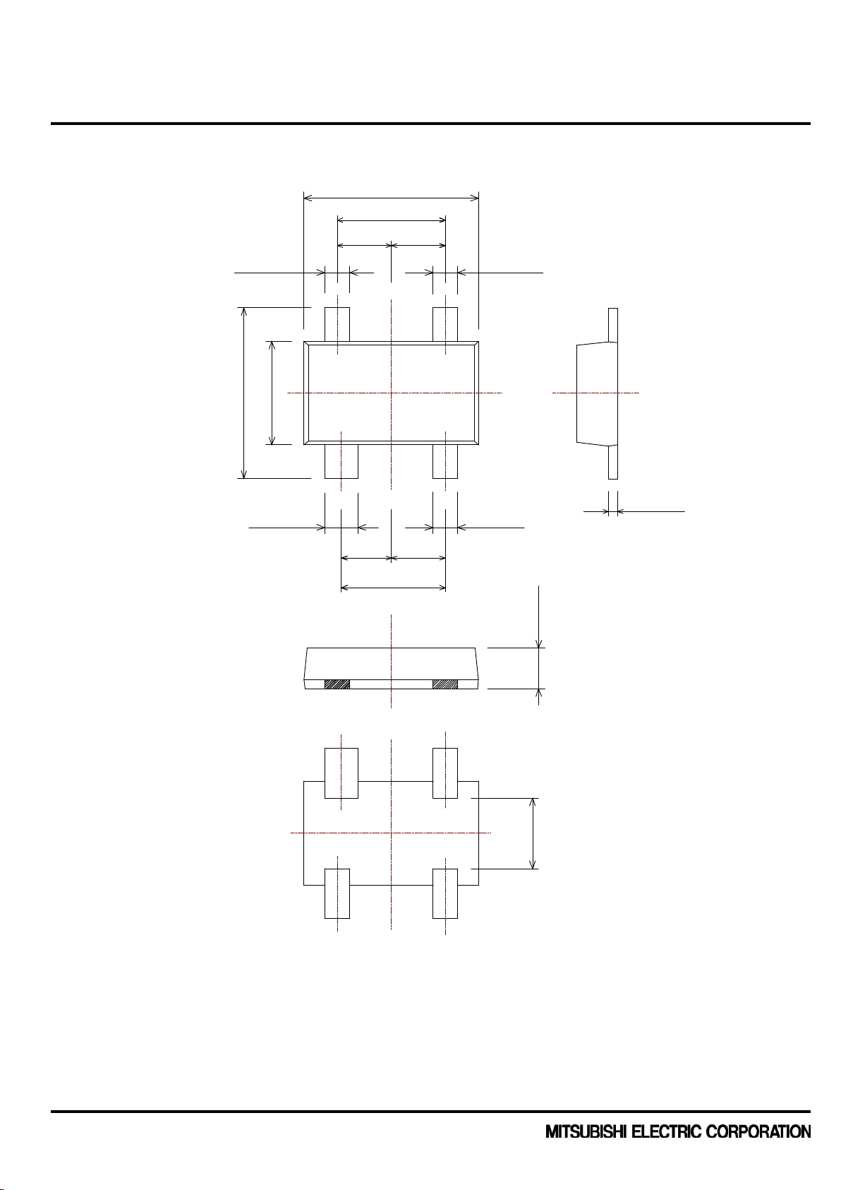
Outline Drawing
Fig.1
Limits Unit
MIN. TYP. MAX
-3.5 -- -- V
-- -- 50 µA
12 -- 60 mA
-0.1 -- -1.5 V
11.0 12.0 -- dB
-- 0.45 0.65 dB
Publication Date : Apr., 2011
1
Page 2
< Low Noise GaAs HEMT >
MGF4935AM
4pin flat lead package
Fig.1
Top
0.30
±0.1
±0.1
+0.1
-0.05
(0.65)
②
2.10
1.30
1.30
±0.1
±0.05
(0.65)
(0.65)
①
0.30
+0.1
-0.05
E □
2.05
1.25
0.40
+0.1
-0.05
③
(0.60)
(0.60)
1.25
1.25
(0.65)
±0.05
②
0.30
+0.1
-0.05
+0.05
-0
0.11
±0.05
0.49
Side
Bottom
③
②
②
①
Unit: mm
(0.85)
① Gate
② Source
③ Drain
(GD-30)
Publication Date : Apr., 2011
2
Page 3

< Low Noise GaAs HEMT >
V
MGF4935AM
4pin flat lead package
TYPICAL CHARACTERISTICS
50
40
(mA )
D
30
20
Drain Current, I
10
2.2
2.0
1.8
1.6
1.4
1.2
1.0
0.8
0.6
Nois e Figure, NF (dB)
0.4
0.2
0.0
IIII
DDDD
vs. V
vs. V
vs. V vs. V
0
0 1 2 3 4
Drain to Sourc e voltage, VDS(V)
NF & Gs vs. I
NF & Gs vs. I
NF & Gs vs. INF & Gs vs. I
Ta=25
=2V
DS
f=12GHz
0 5 10 15 20
DS
DS
IIII
DSDS
DDDD
℃
Drain c urrent, ID (m A )
(Ta=25°C)
15
14
13
12
11
10
9
8
7
6
5
4
DDDD
vs. V
vs. V
vs. V vs. V
50
40
(mA )
D
30
20
Drain Current, I
10
0
-1.0 -0 .5 0.0
Gate to Souc e voltage, VGS(V)
Associated Gain, Gs (dB)
GS
GS
GSGS
(VDS=2V) (VGS=~0.1V/STEP)
Publication Date : Apr., 2011
3
Page 4

< Low Noise GaAs HEMT >
No
te:
MGF4935AM
4pin flat lead package
S PARAMETERS
Freq. S22
(GHz) (mag) (ang) (mag) (ang) (mag) (ang) (mag) (ang)
1 0.990 -13.4 4.592 164.5 0.013 80.2 0.669 -10.6
2 0.964 -26.9 4.545 149.2 0.027 71.6 0.658 -21.3
3 0.923 -40.6 4.476 134.3 0.039 62.7 0.636 -31.2
4 0.866 -54.5 4.463 119.5 0.051 54.6 0.603 -41.8
5 0.804 -68.1 4.370 105.1 0.061 46.8 0.569 -51.7
6 0.734 -82.3 4.241 91.0 0.069 39.3 0.529 -61.1
7 0.659 -96.5 4.113 77.4 0.076 33.2 0.488 -69.7
8 0.582 -111.0 3.965 64.0 0.082 28.2 0.446 -77.6
9 0.507 -126.1 3.804 51.4 0.086 24.0 0.404 -84.9
10 0.438 -142.0 3.660 38.9 0.091 20.9 0.368 -91.9
11 0.381 -158.6 3.548 26.9 0.097 19.0 0.338 -99.5
12 0.340 -178.7 3.440 14.7 0.106 16.9 0.320 -109.4
13 0.319 158.0 3.355 2.2 0.118 13.2 0.303 -120.9
14 0.327 133.9 3.276 -10.8 0.131 8.5 0.300 -137.1
15 0.370 112.0 3.191 -24.0 0.146 2.8 0.307 -157.2
16 0.440 93.2 3.080 -37.9 0.159 -4.2 0.327 179.4
17 0.520 78.4 2.914 -51.9 0.173 -11.5 0.369 157.8
18 0.601 64.0 2.690 -66.0 0.183 -19.4 0.419 137.5
19 0.672 50.4 2.405 -78.6 0.190 -27.1 0.472 122.4
20 0.737 38.9 2.146 -88.9 0.195 -34.2 0.510 110.5
21 0.800 30.7 1.931 -99.1 0.197 -42.0 0.548 98.5
22 0.847 27.2 1.738 -108.8 0.196 -49.0 0.582 83.9
23 0.886 25.8 1.574 -118.1 0.195 -55.9 0.619 68.2
24 0.920 23.1 1.459 -127.4 0.193 -61.4 0.652 52.9
25 0.948 16.5 1.382 -137.6 0.202 -67.4 0.693 40.5
26 0.954 3.1 1.332 -150.9 0.213 -77.2 0.730 31.4
Noise Parameter
We are ready to provide nonlinear model for ADS and MWO users. If you are interested, please contact our sales
offices.
Fr eq. NFmin Rn
(GHz) (dB) (mag) (ang) (Ω )
1 0.20 0.99 3.1 18.0
2 0.20 0.98 8.3 16.5
3 0.21 0.98 14.9 15.0
4 0.22 0.97 20.4 13.5
5 0.24 0.95 30.4 12.0
6 0.26 0.90 41.5 10.5
7 0.29 0.83 52.7 9.0
8 0.31 0.71 68.0 7.0
9 0.34 0.60 83.3 5.5
10 0.37 0.50 99.7 4.0
11 0.40 0.41 117.8 3.0
12 0.44 0.33 137.8 2.5
13 0.47 0.27 162.0 2.5
14 0.51 0.24 -178.1 2.5
Not e ; Rn is normalized by 50 ohm .
(VDS=2V,ID=10mA,Ta=room temperature)
S12S11 S21
(VDS=2V,ID=10mA, Ta=room temperature)
opt
Γ
Reference point
Gate
2.5mm
Board: εr=2.6
Thickness: 0.4mm
(4-
φ
0.4: through-hole)
Reference point
Drain
0.96
45゚
Publication Date : Apr., 2011
4
Page 5

< Low Noise GaAs HEMT >
Freq.
S22
(GHz)
(mag)
(ang)
(mag)
(ang)
(mag)
(ang)
(mag)
(ang)
22
0.942
10.5
0.193
-94.8
0.193
-94.7
0.749
-0.3
26
0.951
-10.3
0.151
-117.4
0.149
-118.2
0.789
-36.1
22
0.970
29.8
0.143
-40.0
0.143
-39.8
0.951
76.5
26
0.960
2.8
0.168
-75.8
0.168
-75.4
0.990
24.2
Note:
MGF4935AM
4pin flat lead package
S PARAMETERS
10 0.896 -155.7 0.235 32.2 0.237 32.2 0.725 67.5
11 0.881 -179.8 0.269 17.4 0.269 17.5 0.732 59.1
12 0.865 154.3 0.292 2.2 0.294 2.2 0.739 51.4
13 0.863 127.9 0.306 -13.3 0.307 -13.6 0.747 44.3
14 0.873 103.1 0.306 -28.4 0.307 -28.4 0.751 36.9
15 0.885 82.6 0.294 -41.6 0.295 -41.5 0.755 29.4
16 0.901 66.1 0.280 -52.6 0.280 -52.5 0.764 22.4
17 0.912 52.7 0.264 -61.5 0.265 -61.5 0.768 16.4
18 0.922 40.6 0.252 -69.0 0.252 -69.0 0.778 12.5
19 0.926 28.9 0.242 -76.7 0.242 -76.8 0.784 11.1
20 0.933 19.0 0.224 -84.1 0.225 -83.9 0.777 10.0
21 0.941 12.3 0.210 -89.8 0.210 -89.2 0.761 6.6
23 0.943 10.3 0.176 -100.3 0.175 -100.9 0.743 -9.5
24 0.958 9.3 0.163 -103.8 0.163 -103.9 0.755 -19.4
25 0.970 3.2 0.158 -109.2 0.157 -109.0 0.781 -28.9
(VDS=0V,VGS=-2V,Ta=room temperature)
Freq. S22
(GHz) (mag) (ang) (mag) (ang) (mag) (ang) (mag) (ang)
10 0.942 -104.7 0.216 -17.7 0.216 -17.8 0.950 -101.6
11 0.938 -119.1 0.221 -32.2 0.220 -32.3 0.942 -114.0
12 0.934 -136.1 0.217 -47.7 0.218 -47.8 0.942 -127.8
13 0.928 -156.1 0.201 -65.7 0.201 -65.7 0.934 -143.2
14 0.935 -178.9 0.170 -85.7 0.169 -85.7 0.941 -161.1
15 0.939 155.9 0.119 -107.4 0.119 -107.2 0.945 179.1
16 0.943 130.2 0.057 -127.3 0.057 -127.6 0.954 158.6
17 0.949 105.8 0.005 -25.0 0.005 -27.7 0.963 139.9
18 0.952 83.3 0.051 6.5 0.050 7.1 0.970 123.7
19 0.957 63.4 0.086 -4.4 0.086 -4.4 0.978 112.1
20 0.963 46.8 0.115 -16.6 0.115 -16.8 0.976 101.9
21 0.972 35.0 0.133 -29.5 0.132 -28.8 0.961 90.3
(VDS=0V,VGS=0V,Ta=room temperature)
S11 S21 S12
1 0.999 -11.6 0.008 97.0 0.008 96.6 0.648 168.2
2 0.996 -24.0 0.018 98.4 0.018 100.0 0.648 156.5
3 0.990 -36.5 0.032 97.9 0.032 98.7 0.652 144.6
4 0.988 -50.0 0.050 94.7 0.050 94.7 0.664 133.1
5 0.981 -64.3 0.073 87.6 0.074 87.8 0.674 121.4
6 0.972 -79.2 0.099 79.4 0.100 79.7 0.682 109.6
7 0.958 -95.5 0.130 69.2 0.130 69.1 0.693 97.9
8 0.944 -113.8 0.165 58.0 0.165 58.2 0.706 87.1
9 0.918 -133.8 0.200 45.6 0.200 45.8 0.717 76.9
S21 S12S11
1 0.997 -9.0 0.022 81.0 0.023 79.7 0.997 -9.9
2 0.997 -18.1 0.045 70.6 0.045 70.6 0.995 -19.8
3 0.997 -27.7 0.068 60.4 0.068 61.1 0.993 -29.2
4 0.993 -37.3 0.092 50.9 0.092 50.6 0.987 -39.0
5 0.988 -47.1 0.116 40.8 0.116 40.9 0.980 -49.4
6 0.985 -57.4 0.139 30.9 0.139 30.6 0.979 -59.2
7 0.972 -68.0 0.162 19.9 0.162 19.8 0.974 -69.1
8 0.973 -79.2 0.184 8.1 0.185 8.1 0.966 -79.5
9 0.956 -91.8 0.201 -4.1 0.202 -4.2 0.957 -89.9
23 0.967 27.0 0.145 -49.6 0.147 -49.5 0.941 61.2
24 0.974 24.0 0.149 -56.9 0.149 -57.0 0.953 46.5
25 0.983 17.1 0.159 -64.6 0.159 -64.7 0.974 33.8
We are ready to provide nonlinear model for ADS and MWO users. If you are interested, please contact our sales
offices.
Publication Date : Apr., 2011
5
Page 6

< Low Noise GaAs HEMT >
MGF4935AM
4pin flat lead package
•
Mitsubishi Electric Corporation puts the maximum effort into making semiconductor products better and
more reliable, but there is always the possibility that trouble may occur with them. Trouble with
semiconductors may lead to personal injury, fire ore property damage. Remember to give due
consideration to safety when making your circuit designs, with appropriate measures such as (i) placement
of substitutive, auxiliary circuits, (ii) use of non-flammable material or (iii) prevention against any
malfunction or mishap.
•
These materials are intended as a reference to assist our customers in the selection of the Mitsubishi
semiconductor product best suited to the customer’s application; they do not convey any license under any
intellectual property rights, or any other rights, belonging to Mitsubishi Electric Corporation or a third party.
•
Mitsubishi Electric Corporation assumes no responsibility for any damage, or infringement of any third-
party’s rights, originating in the use of any product data, diagrams, charts, programs, algorithms, or circuit
application examples contained in these materials.
•
All information contained in these materials, including product data, diagrams, charts, programs and
algorithms represents information on products at the time of publication of these materials, and are subject
to change by Mitsubishi Electric Corporation without notice due to product improvements or other reasons.
It is therefore recommended that customers contact Mitsubishi Electric Corporation or an authorized
Mitsubishi Semiconductor product distributor for the latest product information before purchasing a product
listed herein.
The information described here may contain technical in accuracies or typographical errors.
Mitsubishi Electric Corporation assumes no responsibility for any damage, liability, or other loss rising from
these inaccuracies or errors.
Please also pay attention to information published by Mitsubishi Electric Corporation by various means,
including the Mitsubishi Semiconductor home page (http://www.mitsubishielectric.com/).
•
When using any or all of the information contained in these materials, including product data, diagrams,
charts, programs, and algorithms, please be sure to evaluate all information as a total system before
making a final decision on the applicability of the information and products. Mitsubishi Electric Corporation
assumes no responsibility for any damage, liability or other loss resulting from the information contained
herein.
•
Mitsubishi Electric Corporation semiconductors are not designed or manufactured for use in a device or
system that is used under circumstances in which human life is potentially at stake. Please contact
Mitsubishi Electric Corporation or an authorized Mitsubishi Semiconductor product distributor when
considering the use of a product contained herein for any specific purposes, such as apparatus or systems
for transportation, vehicular, medical, aerospace, nuclear, or undersea repeater use.
•
The prior written approval of Mitsubishi Electric Corporation is necessary to reprint or reproduce in whole
ore in part these materials.
•
If these products or technologies are subject to the Japanese export control restrictions, they must be
exported under a license from the Japanese government and cannot be imported into a country other than
the approved destination.
Any diversion or re-export contrary to the export control laws and regulations of Japan and/or the country
of destination is prohibited.
•
Please contact Mitsubishi Electric Corporation or an authorized Mitsubishi Semiconductor product
distributor for further details on these materials or the products contained therein.
© 2011 MITSUBISHI ELECTRIC CORPORATION. ALL RIGHTS RESERVED.
Keep safety first in your circuit designs!
Notes regarding these materials
Publication Date : Apr., 2011
6
 Loading...