

Page 1
< Low Noise GaAs HEMT >
MGF4934CM
4pin flat lead package
DESCRIPTION
The MGF4934CM super-low noise InGaAs HEMT (High Electron Mobility
Transistor) is designed for use in S to Ku band amplifiers.
The 4pin flat lead package is small-thin size, and offers high cost
performance.
FEATURES
Low noise figure @ f=12GHz
NFmin. = 0.50dB (Typ.)
High associated gain @ f=12GHz
Gs = 13.0dB (Typ.)
APPLICATION
S to Ku band low noise amplifiers
QUALITY GRADE
GG
RECOMMENDED BIAS CONDITIONS
VDS=2V , ID=10mA
MITSUBISHI Proprietary
Not to be reproduced or disclosed without
permission by Mitsubishi Electric
ORDERING INFORMATION
General part number: MGF4934CM-75
Tape & reel 15000pcs/reel
RoHS COMPLIANT
MGF4934CM is a RoHS compliant product. RoHS compliance is indicated by the letter “G” after the Lot Marking.
ABSOLUTE MAXIMUM RATINGS
Symbol Parameter Ratings Unit
V
GDO
V
GSO
ID
PT Total power dissipation 50 mW
Tch
T
stg
Gate to drain voltage -3 V
Gate to source voltage -3 V
Drain current IDSS mA
Channel temperature 125 C
Storage temperature -55 to +125 C
ELECTRICAL CHARACTERISTICS
Symbol Parameter Test conditions Limits Unit
MIN. TYP. MAX
V
V
NFmin. Minimum noise figure
Note: Gs and NFmin. are tested with sampling inspection.
(BR)GDO
I
I
GS(off)
Gate to drain breakdown voltage
Gate to source leakage current
GSS
Saturated drain current
DSS
Gate to source cut-off voltage
Gs Associated gain
(Ta=25C )
IG=-10A
VGS=-2V,VDS=0V
VGS=0V,VDS=2V
VDS=2V,ID=500A
VDS=2V,
ID=10mA,f=12GHz
(Ta=25C )
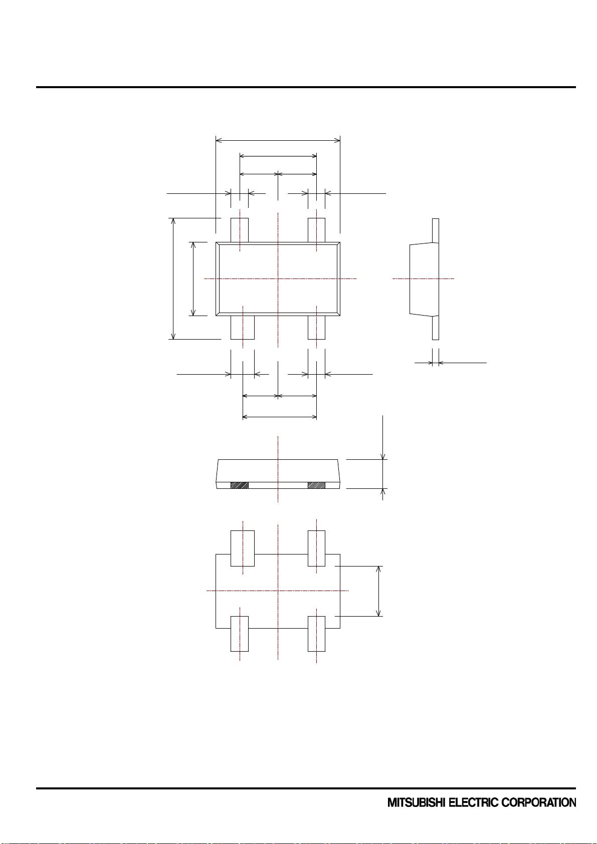
Outline Drawing
Fig.1
-3.5 -- -- V
-- -- 50 A
12 -- 60 mA
-0.1 -- -1.5 V
11.5 13.0 -- dB
-- 0.50 0.75 dB
Publication Date : Apr., 2011
1
Page 2
< Low Noise GaAs HEMT >
MGF4934CM
4pin flat lead package
Fig.1
Top
0.30
±0.1
±0.1
+0.1
-0.05
(0.65)
②
2.10
1.30
1.30
±0.1
±0.05
(0.65)
(0.65)
①
0.30
+0.1
-0.05
D □
2.05
1.25
0.40
+0.1
-0.05
③
(0.60)
(0.60)
1.25
1.25
(0.65)
±0.05
②
0.30
+0.1
-0.05
±0.05
0.49
0.11
+0.05
-0
Side
Bottom
③
②
②
①
(0.85)
Unit: mm
① Gate
② Source
③ Drain
(GD-30)
Publication Date : Apr., 2011
2
Page 3

< Low Noise GaAs HEMT >
MGF4934CM
4pin flat lead package
TYPICAL CHARACTERISTICS
50
40
30
20
10
Drain Current, ID (mA)
0
-1 -0.5 0
Gate to Source Voltage, V
2.20
2.00
1.80
1.60
1.40
1.20
1.00
0.80
0.60
Noise Figure, NF (dB)
0.40
0.20
0.00
Ta =2 5 ℃
VDS=2V
Freq=12GHz
0 5 10 15 20
ID vs. VDS ID vs. VGS
GS=~0.1V/STEP)
(V
NF & Gs vs. ID
Gs
NF
Drain Current, ID (mA)
(Ta=25°C)
GS (V)
50
40
30
20
10
Drain Current, ID (mA)
0
01234
Drain to Source Voltage, V
15
14
13
12
11
10
9
8
7
Associated Gain, Gs (dB)
6
5
4
(VDS=2V)
DS (V)
Publication Date : Apr., 2011
3
Page 4

< Low Noise GaAs HEMT >
MGF4934CM
4pin flat lead package
S PARAMETERS
Freq.
(GHz) (mag) (ang) (mag) (ang) (mag) (ang) (mag) (ang)
1 0.997 -24.9 5.499 155.2 0.031 68.3 0.750 -15.2
2 0.981 -38.3 5.255 141.5 0.037 60.1 0.720 -26.2
3 0.931 -51.7 5.010 127.8 0.043 51.9 0.690 -37.2
4 0.881 -65.1 4.766 114.1 0.049 43.6 0.660 -48.2
5 0.819 -81.5 4.601 98.8 0.057 33.5 0.627 -59.6
6 0.760 -97.5 4.434 83.8 0.062 24.4 0.591 -70.7
7 0.697 -114.1 4.249 68.9 0.065 15.0 0.551 -81.5
8 0.646 -131.5 4.070 54.1 0.070 5.7 0.509 -92.9
9 0.585 -147.6 3.864 40.6 0.068 -2.3 0.467 -102.5
10 0.538 -163.8 3.709 27.4 0.062 -7.5 0.435 -111.8
11 0.516 179.9 3.612 14.5 0.062 -8.9 0.417 -121.6
12 0.498 162.7 3.521 1.4 0.062 -10.4 0.400 -132.4
13 0.491 144.8 3.445 -11.9 0.064 -13.5 0.387 -144.3
14 0.497 128.1 3.424 -25.3 0.064 -13.9 0.392 -155.9
15 0.513 111.8 3.385 -39.3 0.067 -18.8 0.396 -169.8
16 0.547 94.1 3.227 -55.4 0.079 -23.6 0.415 167.7
17 0.579 78.4 3.136 -70.5 0.085 -30.0 0.427 150.4
18 0.611 64.3 2.976 -85.4 0.093 -38.3 0.441 129.8
Noise Parameter
Freq. NFmin Rn
(GHz) (dB) (mag) (ang) (Ω)
1 0.20 0.98 -8.9 16.5
2 0.21 0.95 5.3 15.0
3 0.22 0.89 19.5 13.5
4 0.24 0.82 33.7 12.1
5 0.26 0.76 47.9 10.6
6 0.28 0.69 62.1 9.1
7 0.32 0.63 76.3 7.6
8 0.34 0.56 91.5 6.2
9 0.37 0.50 107.8 4.6
10 0.42 0.45 125.1 3.1
11 0.47 0.41 143.3 2.6
12 0.51 0.38 162.5 2.0
13 0.56 0.35 -177.3 2.0
14 0.61 0.35 -156.2 2.4
15 0.65 0.36 -134.2 3.3
16 0.69 0.39 -111.1 4.8
17 0.74 0.43 -88.1 6.2
18 0.79 0.46 -65.0 7.7
Note:
We are ready to provide nonlinear model for ADS and MWO users. If you are interested, please contact our sales
offices.
(VDS=2V,ID=10mA,Ta=room temperature)
(VDS=2V,ID=10mA, Ta=room temperature)
opt
S22S11 S21 S12
Measurement plane (2.5mm)
Recommended foot pattern;
RO4003C/Rogers (r=3.38, t=0.508mm)
Publication Date : Apr., 2011
4
Page 5

< Low Noise GaAs HEMT >
MGF4934CM
4pin flat lead package
S PARAMETERS
(VDS=2V,ID=10mA,Ta=room temperature)
Noise Parameter
(VDS=2V,ID=10mA, Ta=room temperature))
Note:
We are ready to provide nonlinear model for ADS and MWO users. If you are interested, please contact our sales
offices.
Freq.
(GHz) (mag) (ang) (mag) (ang) (mag) (ang) (mag) (ang)
1 0.990 -16.3 5.156 158.7 0.032 79.5 0.758 -9.2
2 0.985 -30.1 4.971 145.3 0.037 70.2 0.728 -19.5
3 0.930 -43.8 4.787 131.9 0.042 60.9 0.698 -29.9
4 0.860 -57.5 4.602 118.5 0.047 51.6 0.668 -40.3
5 0.802 -72.1 4.470 103.9 0.055 43.4 0.634 -50.0
6 0.737 -87.3 4.343 89.3 0.061 36.2 0.594 -59.5
7 0.668 -103.2 4.212 74.6 0.066 29.7 0.555 -68.9
8 0.599 -119.6 4.042 60.2 0.070 24.0 0.514 -78.3
9 0.533 -136.5 3.852 46.4 0.072 18.9 0.473 -87.3
10 0.477 -152.0 3.672 33.9 0.072 17.3 0.440 -95.2
11 0.442 -168.0 3.537 21.6 0.076 17.1 0.418 -104.2
12 0.421 175.7 3.429 9.5 0.083 17.2 0.400 -114.1
13 0.406 159.0 3.331 -2.4 0.090 15.9 0.383 -124.4
14 0.405 142.8 3.264 -14.1 0.099 14.1 0.375 -135.6
15 0.425 126.5 3.236 -26.9 0.115 10.1 0.379 -150.3
16 0.460 110.8 3.214 -40.8 0.137 5.3 0.403 -168.9
17 0.503 94.9 3.149 -54.5 0.156 -2.2 0.417 172.6
18 0.547 80.2 3.058 -68.3 0.175 -11.2 0.448 153.5
opt
Freq. NFmin Rn
(GHz) (dB) (mag) (ang) (Ω)
1 0.25 0.97 8.2 17.5
2 0.25 0.97 14.5 15.4
3 0.26 0.94 22.9 14.0
4 0.29 0.91 30.2 12.5
5 0.30 0.88 40.2 11.0
6 0.32 0.82 48.2 9.5
7 0.35 0.74 61.2 8.0
8 0.37 0.65 75.5 6.5
9 0.39 0.57 91.3 5.0
10 0.42 0.49 108.4 3.6
11 0.46 0.44 127.0 2.6
12 0.49 0.39 146.9 1.9
13 0.53 0.34 168.2 1.8
14 0.57 0.30 -169.1 2.0
Reference point
Gate
S22S11 S21 S12
2.5mm
Board: r=2.6
Thickness: 0.4mm
(4-φ0.4: through-hole)
Reference point
Drain
0.96
45゚
Publication Date : Apr., 2011
5
Page 6

< Low Noise GaAs HEMT >
MGF4934CM
4pin flat lead package
Mitsubishi Electric Corporation puts the maximum effort into making semiconductor products better and
more reliable, but there is always the possibility that trouble may occur with them. Trouble with
semiconductors may lead to personal injury, fire ore property damage. Remember to give due
consideration to safety when making your circuit designs, with appropriate measures such as (i) placement
of substitutive, auxiliary circuits, (ii) use of non-flammable material or (iii) prevention against any
malfunction or mishap.
These materials are intended as a reference to assist our customers in the selection of the Mitsubishi
semiconductor product best suited to the customer’s application; they do not convey any license under any
intellectual property rights, or any other rights, belonging to Mitsubishi Electric Corporation or a third party.
Mitsubishi Electric Corporation assumes no responsibility for any damage, or infringement of any third-
party’s rights, originating in the use of any product data, diagrams, charts, programs, algorithms, or circuit
application examples contained in these materials.
All information contained in these materials, including product data, diagrams, charts, programs and
algorithms represents information on products at the time of publication of these materials, and are subject
to change by Mitsubishi Electric Corporation without notice due to product improvements or other reasons.
It is therefore recommended that customers contact Mitsubishi Electric Corporation or an authorized
Mitsubishi Semiconductor product distributor for the latest product information before purchasing a product
listed herein.
The information described here may contain technical in accuracies or typographical errors.
Mitsubishi Electric Corporation assumes no responsibility for any damage, liability, or other loss rising from
these inaccuracies or errors.
Please also pay attention to information published by Mitsubishi Electric Corporation by various means,
including the Mitsubishi Semiconductor home page (http://www.mitsubishielectric.com/).
When using any or all of the information contained in these materials, including product data, diagrams,
charts, programs, and algorithms, please be sure to evaluate all information as a total system before
making a final decision on the applicability of the information and products. Mitsubishi Electric Corporation
assumes no responsibility for any damage, liability or other loss resulting from the information contained
herein.
Mitsubishi Electric Corporation semiconductors are not designed or manufactured for use in a device or
system that is used under circumstances in which human life is potentially at stake. Please contact
Mitsubishi Electric Corporation or an authorized Mitsubishi Semiconductor product distributor when
considering the use of a product contained herein for any specific purposes, such as apparatus or systems
for transportation, vehicular, medical, aerospace, nuclear, or undersea repeater use.
The prior written approval of Mitsubishi Electric Corporation is necessary to reprint or reproduce in whole
ore in part these materials.
If these products or technologies are subject to the Japanese export control restrictions, they must be
exported under a license from the Japanese government and cannot be imported into a country other than
the approved destination.
Any diversion or re-export contrary to the export control laws and regulations of Japan and/or the country
of destination is prohibited.
Please contact Mitsubishi Electric Corporation or an authorized Mitsubishi Semiconductor product
distributor for further details on these materials or the products contained therein.
© 2011 MITSUBISHI ELECTRIC CORPORATION. ALL RIGHTS RESERVED.
Keep safety first in your circuit designs!
Notes regarding these materials
Publication Date : Apr., 2011
6
 Loading...