

Page 1
< Low Noise GaAs HEMT >
MGF4934BM
4pin flat lead package
DESCRIPTION
The MGF4934BM super-low noise InGaAs HEMT (High Electron Mobility
Transistor) is designed for use in S to Ku band amplifiers.
The 4pin flat lead package is small-thin size, and offers high cost
performance.
FEATURES
Low noise figure @ f=12GHz
NFmin. = 0.50dB (Typ.)
High associated gain @ f=12GHz
Gs = 12.5dB (Typ.)
APPLICATION
S to Ku band low noise amplifiers
QUALITY GRADE
GG
RECOMMENDED BIAS CONDITIONS
VDS=2V , ID=10mA
MITSUBISHI Proprietary
Not to be reproduced or disclosed without
permission by Mitsubishi Electric
ORDERING INFORMATION
General part number: MGF4934BM-75
Tape & reel 15000pcs/reel
RoHS COMPLIANT
MGF4934BM is a RoHS compliant product. RoHS compliance is indicated by the letter “G” after the Lot Marking.
ABSOLUTE MAXIMUM RATINGS
Symbol Parameter Ratings Unit
V
GDO
V
GSO
ID
PT Total power dissipation 50 mW
Tch
T
stg
Gate to drain voltage -3 V
Gate to source voltage -3 V
Drain current IDSS mA
Channel temperature 125 C
Storage temperature -55 to +125 C
ELECTRICAL CHARACTERISTICS
Symbol Parameter Test conditions Limits Unit
MIN. TYP. MAX
V
V
NFmin. Minimum noise figure
Note: Gs and NFmin. are tested with sampling inspection.
(BR)GDO
I
I
GS(off)
Gate to drain breakdown voltage
Gate to source leakage current
GSS
Saturated drain current
DSS
Gate to source cut-off voltage
Gs Associated gain
(Ta=25C )
IG=-10A
VGS=-2V,VDS=0V
VGS=0V,VDS=2V
VDS=2V,ID=500A
VDS=2V,
ID=10mA,f=12GHz
(Ta=25C )
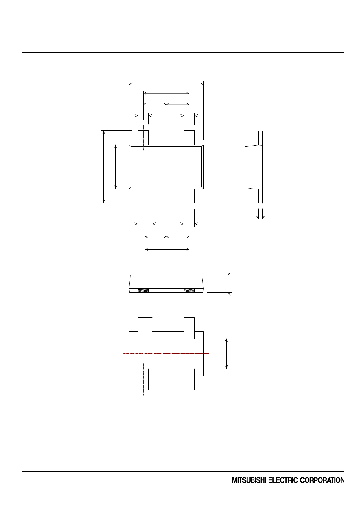
Outline Drawing
Fig.1
-3.5 -- -- V
-- -- 50 A
12 -- 60 mA
-0.1 -- -1.5 V
11.5 12.5 -- dB
-- 0.50 0.80 dB
Publication Date : Apr., 2011
1
Page 2
< Low Noise GaAs HEMT >
MGF4934BM
4pin flat lead package
Fig.1
Top
0.30
±0.1
±0.1
+0.1
-0.05
(0.65)
②
2.10
1.30
1.30
±0.1
±0.05
(0.65)
(0.65)
①
0.30
+0.1
-0.05
B □
2.05
1.25
0.40
+0.1
-0.05
③
(0.60)
(0.60)
1.25
1.25
(0.65)
±0.05
②
0.30
+0.1
-0.05
±0.05
0.49
0.11
+0.05
-0
Side
Bottom
③
②
②
①
(0.85)
Unit: mm
① Gate
② Source
③ Drain
(GD-30)
Publication Date : Apr., 2011
2
Page 3

< Low Noise GaAs HEMT >
MGF4934BM
4pin flat lead package
TYPICAL CHARACTERISTICS
50
40
(mA)
D
30
20
Drain Current, I
10
0
01234
2.2
Ta=25
2.0
VDS=2V
1.8
f=12GHz
1.6
1.4
1.2
1.0
0.8
0.6
Noise Figure, NF (dB)
0.4
0.2
0.0
0 5 10 15 20
ID vs. VDS ID vs. VGS
GS=~0.1V/STEP)
(V
Drain to Source voltage, VDS(V)
NF & Gs vs. ID
℃
Gs
NF
Drain Current, ID (mA)
(Ta=25°C)
Gs
NF
50
40
(mA)
D
30
20
Drain Current, I
10
0
-1.0 -0.5 0.0
Gate to Souce voltage, VGS(V)
15
14
13
12
11
10
9
8
7
6
Associated Gain, Gs (dB)
5
4
(VDS=2V)
Publication Date : Apr., 2011
3
Page 4

< Low Noise GaAs HEMT >
MGF4934BM
4pin flat lead package
S PARAMETERS
Freq.
(GHz) (mag) (ang) (mag) (ang) (mag) (ang) (mag) (ang)
1 0.986 -14.0 4.534 163.6 0.014 79.1 0.676 -11.0
2 0.961 -27.8 4.478 148.2 0.027 70.5 0.663 -22.3
3 0.918 -41.9 4.394 132.8 0.038 61.9 0.638 -32.7
4 0.863 -59.4 4.523 116.2 0.052 50.3 0.580 -45.1
5 0.808 -72.1 4.309 102.2 0.060 43.3 0.559 -53.8
6 0.748 -85.2 4.148 88.6 0.067 36.9 0.530 -62.2
7 0.683 -98.1 4.015 75.1 0.073 30.5 0.496 -70.0
8 0.613 -111.9 3.860 61.9 0.078 25.3 0.454 -76.5
9 0.543 -126.8 3.744 49.0 0.082 20.9 0.411 -83.1
10 0.474 -142.9 3.644 35.8 0.087 17.1 0.364 -91.0
11 0.421 -160.9 3.552 22.8 0.092 14.0 0.321 -100.6
12 0.395 177.9 3.488 9.6 0.100 11.1 0.278 -114.7
13 0.395 154.9 3.396 -4.0 0.111 7.6 0.239 -133.9
14 0.433 132.9 3.295 -17.6 0.122 2.2 0.214 -159.5
15 0.491 114.0 3.183 -31.5 0.133 -4.2 0.219 170.8
16 0.559 97.5 3.056 -45.9 0.144 -11.1 0.256 144.4
17 0.630 83.0 2.886 -60.6 0.154 -18.6 0.315 122.4
18 0.692 70.3 2.662 -74.9 0.161 -26.6 0.379 104.1
19 0.739 60.2 2.401 -87.7 0.169 -34.2 0.440 88.4
20 0.787 52.4 2.198 -98.5 0.174 -42.1 0.484 73.6
21 0.828 45.4 2.060 -109.9 0.179 -50.4 0.527 60.5
22 0.866 39.4 1.940 -120.6 0.180 -58.5 0.575 47.9
23 0.894 33.7 1.810 -131.4 0.183 -65.4 0.632 35.7
24 0.921 26.1 1.710 -142.1 0.184 -71.5 0.695 25.4
25 0.937 16.9 1.632 -152.9 0.187 -78.0 0.770 16.7
26 0.936 5.9 1.541 -165.3 0.186 -86.0 0.846 8.8
Noise Parameter
Freq. NFmin Rn
(GHz) (dB) (mag) (ang) ()
1 0.25 0.99 7.2 17.0
2 0.26 0.98 11.1 15.5
3 0.27 0.95 18.0 13.5
4 0.29 0.92 27.4 12.0
5 0.31 0.89 38.5 10.5
6 0.33 0.82 53.1 9.0
7 0.36 0.75 68.2 7.5
8 0.38 0.67 83.3 6.0
9 0.41 0.60 100.2 4.5
10 0.43 0.53 115.2 3.0
11 0.48 0.47 131.4 2.0
12 0.51 0.42 150.3 1.5
13 0.54 0.37 167.7 1.5
14 0.58 0.35 -178.8 1.5
(VDS=2V,ID=10mA,Ta=room temperature)
S11 S21 S12 S22
(VDS=2V,ID=10mA, Ta=room temperature))
opt
Reference point
Gate
Reference point
Drain
0.96
45゚
2.5mm
Board: r=2.6
Thickness: 0.4mm
(4-φ0.4: through-hole)
Note:
We are ready to provide nonlinear model for ADS and MWO users. If you are interested, please contact our sales
offices.
Publication Date : Apr., 2011
4
Page 5

< Low Noise GaAs HEMT >
MGF4934BM
4pin flat lead package
S PARAMETERS
(VDS=0V,VGS=0V,Ta=room temperature)
(VDS=0V,VGS=-2.5V,Ta=room temperature)
Freq. S22
(GHz) (mag) (ang) (mag) (ang) (mag) (ang) (mag) (ang)
1 0.995 -12.5 0.008 96.4 0.008 97.7 0.673 165.1
2 0.990 -24.6 0.018 100.5 0.018 100.7 0.673 152.1
3 0.991 -37.5 0.032 99.5 0.032 98.9 0.671 138.7
4 0.983 -53.3 0.051 92.5 0.051 94.0 0.694 127.4
5 0.976 -67.1 0.074 85.0 0.075 85.5 0.697 112.5
6 0.961 -81.0 0.099 76.0 0.100 76.5 0.704 97.6
7 0.951 -95.7 0.130 65.5 0.131 65.3 0.719 83.4
8 0.940 -112.3 0.163 53.6 0.163 54.3 0.730 70.8
9 0.913 -130.9 0.196 41.0 0.198 41.3 0.745 59.2
10 0.902 -151.8 0.229 27.1 0.230 27.3 0.759 49.3
11 0.887 -175.9 0.256 12.0 0.257 12.7 0.774 41.2
12 0.883 159.0 0.274 -2.5 0.273 -2.7 0.783 34.8
13 0.884 134.4 0.276 -16.9 0.278 -17.2 0.794 29.2
14 0.889 112.1 0.268 -30.5 0.270 -30.2 0.800 24.0
15 0.896 93.6 0.257 -42.0 0.256 -42.0 0.807 18.7
16 0.907 78.5 0.241 -51.5 0.241 -51.1 0.811 13.2
17 0.911 66.4 0.228 -59.6 0.227 -59.8 0.807 7.1
18 0.919 55.9 0.221 -67.5 0.221 -67.4 0.815 0.6
19 0.924 47.1 0.217 -76.6 0.218 -76.5 0.817 -6.9
20 0.919 38.7 0.204 -87.1 0.204 -86.9 0.814 -14.8
21 0.921 31.2 0.192 -95.0 0.193 -95.3 0.810 -23.2
22 0.924 24.3 0.179 -103.1 0.179 -103.2 0.811 -31.2
23 0.928 18.1 0.168 -110.3 0.168 -110.6 0.817 -39.2
24 0.950 11.6 0.159 -116.7 0.157 -116.3 0.816 -46.5
25 0.970 5.4 0.149 -122.1 0.150 -122.1 0.830 -53.8
26 0.978 -1.5 0.141 -128.2 0.141 -128.3 0.844 -61.8
Freq. S22
(GHz) (mag) (ang) (mag) (ang) (mag) (ang) (mag) (ang)
1 0.993 -9.6 0.022 78.7 0.022 79.0 0.998 -10.6
2 0.996 -18.9 0.044 68.6 0.044 68.8 1.000 -21.3
3 0.992 -28.3 0.065 59.8 0.065 59.2 0.991 -31.2
4 0.987 -39.7 0.092 48.4 0.092 48.4 0.984 -42.1
5 0.981 -49.5 0.112 38.8 0.112 38.8 0.986 -51.5
6 0.975 -59.1 0.131 28.8 0.130 29.1 0.980 -60.6
7 0.968 -68.8 0.150 19.2 0.150 19.2 0.975 -70.1
8 0.963 -79.2 0.169 7.7 0.168 8.0 0.968 -80.7
9 0.949 -89.9 0.185 -4.5 0.186 -4.3 0.959 -92.1
10 0.943 -102.2 0.200 -18.4 0.200 -18.5 0.949 -105.6
11 0.932 -117.2 0.209 -34.7 0.209 -34.4 0.943 -121.1
12 0.929 -134.6 0.207 -52.4 0.207 -52.8 0.932 -139.6
13 0.932 -155.8 0.187 -73.4 0.188 -73.6 0.928 -160.7
14 0.938 -179.2 0.148 -96.3 0.149 -96.7 0.942 176.8
15 0.940 156.2 0.091 -119.2 0.091 -119.3 0.947 153.6
16 0.948 133.1 0.033 -137.6 0.034 -136.8 0.953 132.4
17 0.951 112.7 0.018 9.9 0.018 9.0 0.957 112.9
18 0.952 95.4 0.058 0.6 0.058 0.5 0.965 94.8
19 0.956 80.9 0.091 -11.2 0.090 -11.3 0.964 79.2
20 0.951 68.1 0.117 -24.5 0.118 -24.3 0.960 64.6
21 0.953 57.2 0.138 -37.5 0.137 -37.3 0.954 50.5
22 0.946 47.5 0.150 -49.7 0.150 -49.6 0.947 37.4
23 0.950 38.8 0.157 -60.4 0.157 -60.2 0.952 24.9
24 0.965 30.8 0.161 -69.7 0.161 -70.1 0.963 13.3
25 0.982 23.3 0.162 -77.8 0.162 -77.6 0.981 1.6
26 0.993 15.4 0.163 -85.8 0.163 -85.8 0.995 -10.3
S11 S21 S12
S11 S21 S12
Note:
We are ready to provide nonlinear model for ADS and MWO users. If you are interested, please contact our sales
offices.
Publication Date : Apr., 2011
5
Page 6

< Low Noise GaAs HEMT >
MGF4934BM
4pin flat lead package
Mitsubishi Electric Corporation puts the maximum effort into making semiconductor products better and
more reliable, but there is always the possibility that trouble may occur with them. Trouble with
semiconductors may lead to personal injury, fire ore property damage. Remember to give due
consideration to safety when making your circuit designs, with appropriate measures such as (i) placement
of substitutive, auxiliary circuits, (ii) use of non-flammable material or (iii) prevention against any
malfunction or mishap.
These materials are intended as a reference to assist our customers in the selection of the Mitsubishi
semiconductor product best suited to the customer’s application; they do not convey any license under any
intellectual property rights, or any other rights, belonging to Mitsubishi Electric Corporation or a third party.
Mitsubishi Electric Corporation assumes no responsibility for any damage, or infringement of any third-
party’s rights, originating in the use of any product data, diagrams, charts, programs, algorithms, or circuit
application examples contained in these materials.
All information contained in these materials, including product data, diagrams, charts, programs and
algorithms represents information on products at the time of publication of these materials, and are subject
to change by Mitsubishi Electric Corporation without notice due to product improvements or other reasons.
It is therefore recommended that customers contact Mitsubishi Electric Corporation or an authorized
Mitsubishi Semiconductor product distributor for the latest product information before purchasing a product
listed herein.
The information described here may contain technical in accuracies or typographical errors.
Mitsubishi Electric Corporation assumes no responsibility for any damage, liability, or other loss rising from
these inaccuracies or errors.
Please also pay attention to information published by Mitsubishi Electric Corporation by various means,
including the Mitsubishi Semiconductor home page (http://www.mitsubishielectric.com/).
When using any or all of the information contained in these materials, including product data, diagrams,
charts, programs, and algorithms, please be sure to evaluate all information as a total system before
making a final decision on the applicability of the information and products. Mitsubishi Electric Corporation
assumes no responsibility for any damage, liability or other loss resulting from the information contained
herein.
Mitsubishi Electric Corporation semiconductors are not designed or manufactured for use in a device or
system that is used under circumstances in which human life is potentially at stake. Please contact
Mitsubishi Electric Corporation or an authorized Mitsubishi Semiconductor product distributor when
considering the use of a product contained herein for any specific purposes, such as apparatus or systems
for transportation, vehicular, medical, aerospace, nuclear, or undersea repeater use.
The prior written approval of Mitsubishi Electric Corporation is necessary to reprint or reproduce in whole
ore in part these materials.
If these products or technologies are subject to the Japanese export control restrictions, they must be
exported under a license from the Japanese government and cannot be imported into a country other than
the approved destination.
Any diversion or re-export contrary to the export control laws and regulations of Japan and/or the country
of destination is prohibited.
Please contact Mitsubishi Electric Corporation or an authorized Mitsubishi Semiconductor product
distributor for further details on these materials or the products contained therein.
© 2011 MITSUBISHI ELECTRIC CORPORATION. ALL RIGHTS RESERVED.
Keep safety first in your circuit designs!
Notes regarding these materials
Publication Date : Apr., 2011
6
 Loading...