

Page 1
MITSUBISHI Proprietary
< Power GaAs HEMT >
MGF4851A
Leadless ceramic package
DESCRIPTION
The MGF4851A power InGaAs HEMT (High Electron Mobility Transistor)
is designed for use in S to K band amplifiers.
The lead-less ceramic package assures minimum parasitic losses.
FEATURES
High gain and High P1dB
Glp=11dB , P1dB=14.5dBm (Typ.) @ f=12GHz
APPLICATION
S to K band low noise amplifiers
QUALITY GRADE
GG
RECOMMENDED BIAS CONDITIONS
VDS=2.5V , ID=25mA
Not to be reproduced or disclosed without
permission by Mitsubishi Electric
ORDERING INFORMATION
Tape & reel 3,000pcs/reel
RoHS COMPLIANT
MGF4851A is a RoHS compliant product. RoHS compliance is indicated by the letter “G” after the Lot Marking.
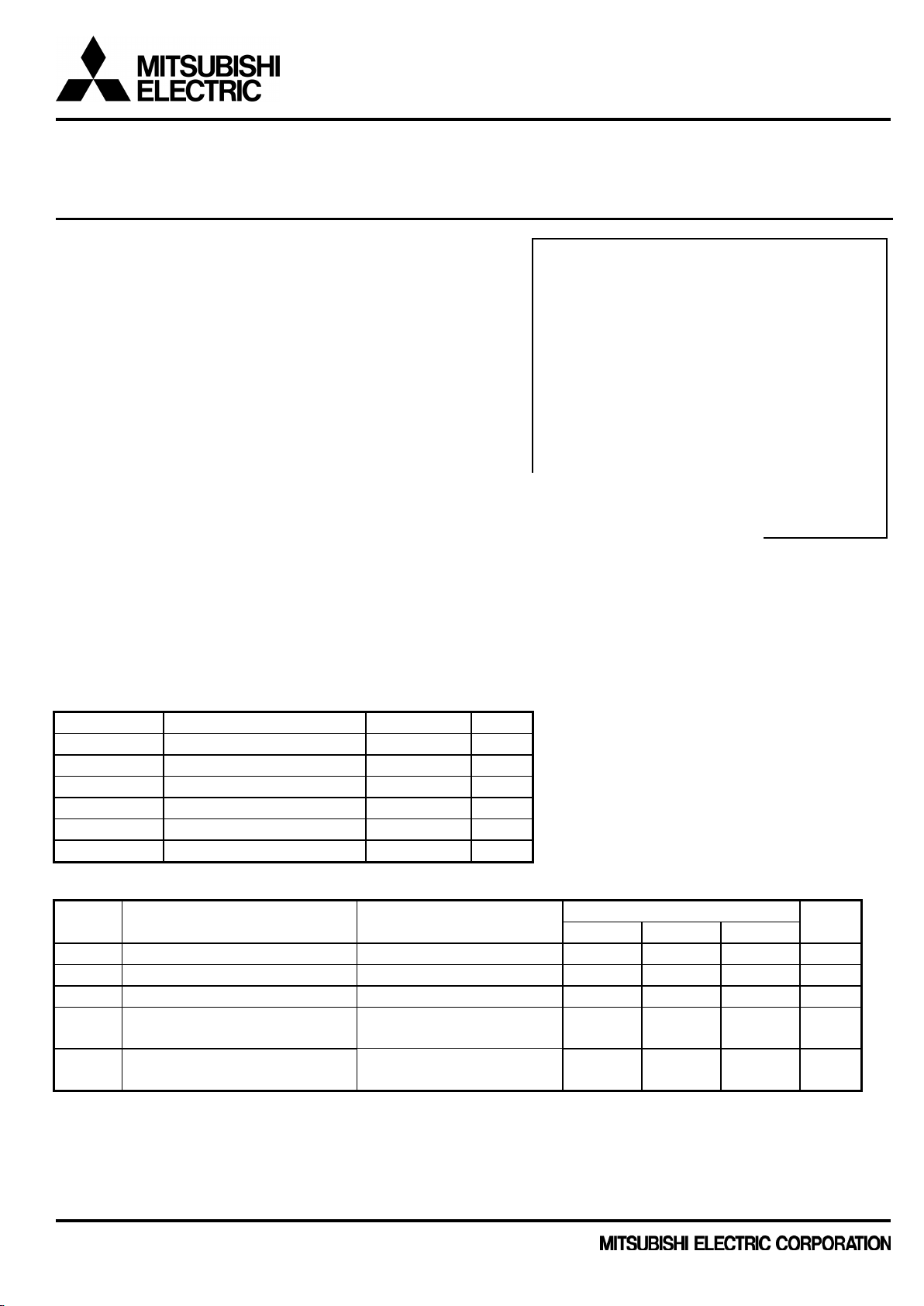
ABSOLUTE MAXIMUM RATINGS
Symbol Parameter Ratings Unit
V
GDO
V
GSO
ID
PT Total power dissipation 100 mW
Tch
T
stg
Gate to drain voltage -5 V
Gate to source voltage -5 V
Drain current IDSS mA
Channel temperature 125 °C
Storage temperature -65 to +125 °C
(Ta=25°C )
ELECTRICAL CHARACTERISTICS
Symbol
V
(BR)GDO
I
V
GS(off)
P1dB Output Power at 1dB gain
Glp Linear Power Gain
Note: P1dB and Glp are tested with sampling inspection.
Gate to drain breakdown voltage
Saturated drain current
DSS
Gate to source cut-off voltage
Compression
Parameter Test conditions
IG=-10µA
VGS=0V,VDS=2.5V
VDS=2.5V,ID=500µA
VDS=2.5V,ID=25mA
f=12GHz
VDS=2.5V,ID=25mA
f=12GHz,Pin=-5dBm
(Ta=25°C )
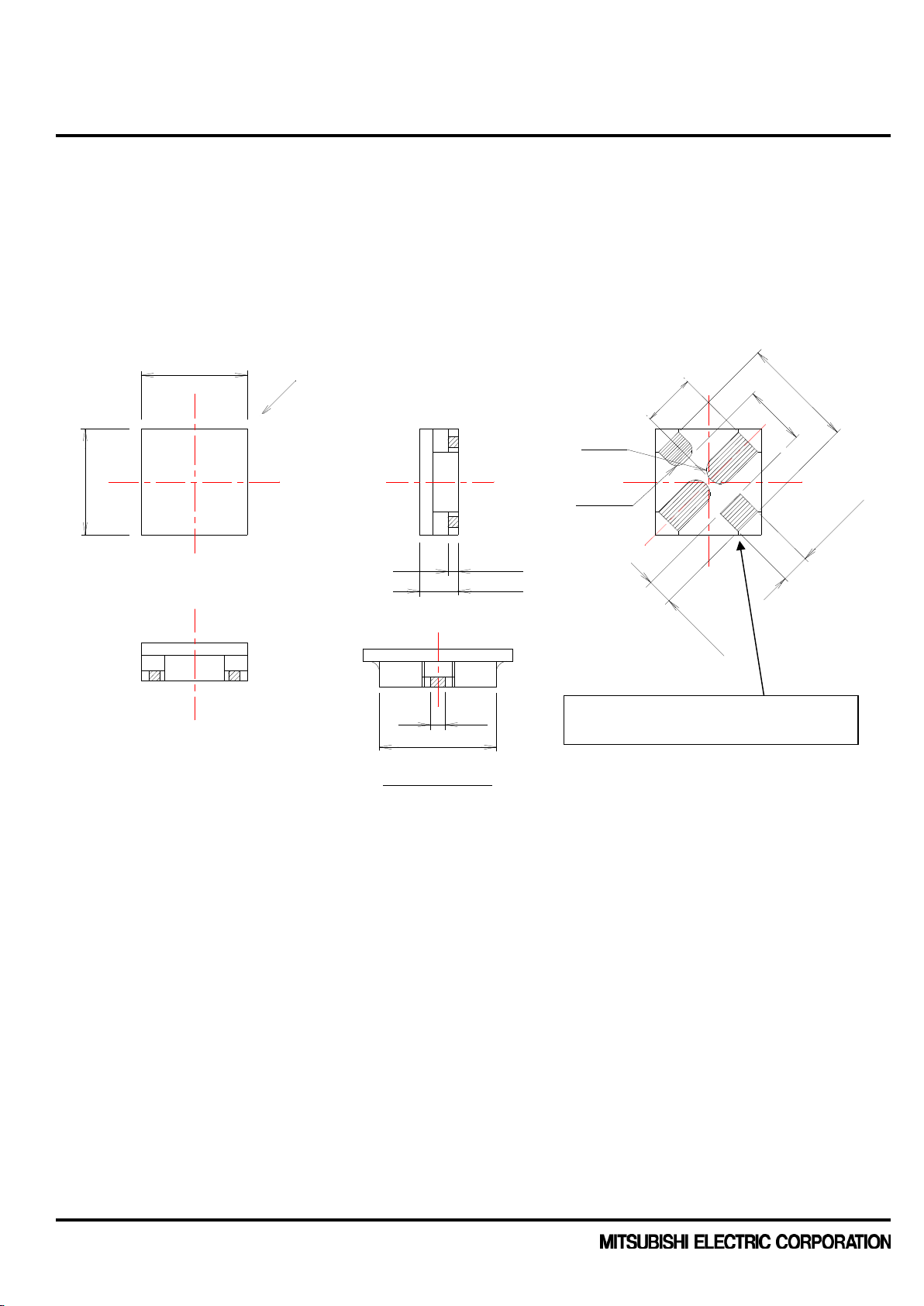
Outline Drawing
Fig.1
Limits Unit
MIN. TYP. MAX
-3 -- -- V
30 60 120 mA
-0.1 -0.8 -2.0 V
12 14.5 -- dBm
9 11 -- dB
Publication Date : Apr., 2011
1
Page 2
< Power GaAs HEMT >
ℵ
ℑ
ℵ
ℑ
G
7
1 A A
MGF4851A
Leadless ceramic package
Fig.1
Top
+0.20
-0.102.15
A
②
①
0
0
2
1
.
.
0
0
+
-
5
1
.
2
③
②
Side
0.20±0.1
0.80±0.1
2-R0.275
2-R0.20
①
②
Bottom
)
2
0
.
1
(
-
2
2
-
0
2
-
(
2
②
.
2
1
0
.
)
2
0
±
0
.
0
5
5
0
.
③
.
5
0
±
0
.
0
5
0
±
5
5
.
0
-
4
(0.30)
(2.30)
from "A" side view
Square shape electrode is Drain
Unit: mm
① Gate
② Source
③ Drain
Publication Date : Apr., 2011
2
Page 3
< Power GaAs HEMT >
MGF4851A
Leadless ceramic package
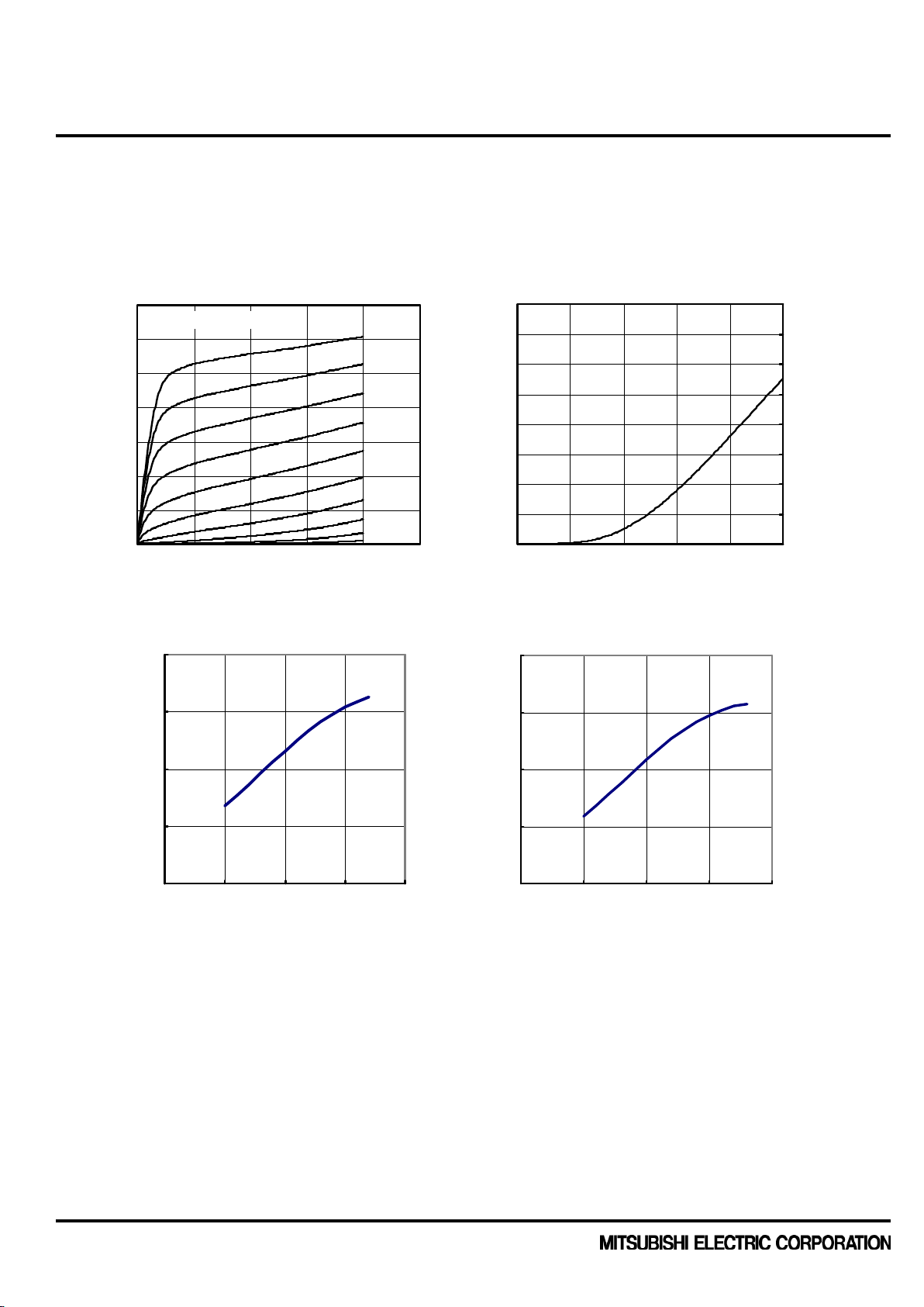
TYPICAL CHARACTERISTICS
70
VGS=-0.1V/STEP
60
50
(mA)
D
40
30
20
DRAIN CURRENT I
10
0
0 1 2 3 4 5
DRAIN TO SOURCE VOLTAGE VDS(V)
20.00
15.00
VDS=2.5V
ID=25mA
f=12GHz
10.00
5.00
Output Power Po (dBm)
0.00
-10 -5 0 5 10
ID vs. VDS
Po vs. Pin
Input Power Pin (dBm)
(Ta=25°C)
VGS=0V
ID vs. VGS
80
VDS=2V
70
60
(mA)
D
I
50
40
30
20
DRAIN CURRENT
10
0
-1.0 -0.8 -0.6 -0.4 -0.2 0.0
GATE TO SOURCE VOLTAGE VGS(V)
Po vs. Pin
20
VDS=2V
ID=10mA
f=12GHz
15
10
5
Output Power Pout (dBm)
0
-10 -5 0 5 10
Input Power Pin (dBm)
Publication Date : Apr., 2011
3
Page 4

< Power GaAs HEMT >
Note:
offices.
(GHz)
(mag)
(ang)
(mag)
(ang)
(mag)
(ang)
(mag)
(ang)
26
0.908
-73.2
1.625
171.0
0.068
171.0
0.530
-73.6
MGF4851A
Leadless ceramic package
S PARAMETERS
]
Freq.
1 0.988 -17.6 5.833 163.3 0.014 76.8 0.550 -14.2
2 0.969 -34.6 5.713 147.5 0.028 64.2 0.543 -28.1
3 0.942 -51.1 5.536 132.3 0.040 52.7 0.534 -41.2
4 0.908 -67.4 5.339 117.4 0.052 40.8 0.519 -53.9
5 0.874 -82.6 5.125 103.4 0.061 30.1 0.508 -65.4
6 0.841 -97.4 4.942 89.7 0.070 19.8 0.494 -76.3
7 0.806 -111.9 4.769 76.2 0.078 9.8 0.478 -86.7
8 0.766 -126.6 4.603 62.7 0.086 -0.2 0.455 -97.5
9 0.714 -140.8 4.408 50.2 0.091 -12.4 0.415 -107.0
10 0.670 -154.5 4.277 37.8 0.093 -22.2 0.384 -115.3
11 0.638 -169.3 4.211 25.3 0.096 -31.4 0.351 -124.1
12 0.608 174.5 4.176 12.4 0.099 -40.7 0.318 -132.9
13 0.581 157.3 4.131 -0.9 0.102 -49.9 0.274 -143.7
14 0.569 137.4 4.114 -15.3 0.106 -61.5 0.226 -153.8
15 0.565 115.0 4.038 -30.5 0.103 -71.2 0.184 -165.4
16 0.566 91.9 3.890 -45.6 0.106 -79.8 0.130 177.0
17 0.592 69.4 3.763 -60.3 0.109 -91.6 0.085 130.2
18 0.624 48.6 3.608 -76.1 0.108 -103.7 0.075 59.9
19 0.680 28.2 3.372 -92.2 0.107 -116.0 0.132 18.2
20 0.739 7.7 3.099 -107.8 0.100 -129.0 0.188 -4.6
21 0.771 -9.2 2.815 -122.3 0.093 -138.2 0.251 -20.0
22 0.818 -23.0 2.576 -136.1 0.093 -149.6 0.314 -32.0
23 0.863 -38.7 2.313 -151.8 0.087 -160.1 0.394 -44.3
24 0.877 -51.5 2.018 -165.3 0.077 -173.8 0.447 -56.9
25 0.893 -63.1 1.799 -177.3 0.069 176.9 0.499 -66.2
(VDS=2.5V,ID=25mA,Ta=room temperature)
S22S11 S21 S12
Measurement plane (2.2mm)
Recommended foot pattern; RO4350B/ROGERS(εr=3.48, t=0.254mm)
We are ready to provide nonlinear model for ADS and MWO users. If you are interested, please contact our sales
Publication Date : Apr., 2011
4
Page 5

< Power GaAs HEMT >
(GHz)
Note
MGF4851A
Leadless ceramic package
S PARAMETERS
10 0.744 -123.4 4.500 66.5 0.083 10.6 0.483 -81.1
11 0.709 -133.5 4.514 57.5 0.092 3.1 0.468 -86.3
12 0.658 -146.0 4.549 47.0 0.099 -4.6 0.437 -91.4
13 0.607 -160.7 4.589 36.3 0.106 -12.3 0.392 -97.5
14 0.561 176.4 4.607 20.9 0.113 -25.3 0.324 -109.3
15 0.523 151.0 4.547 7.2 0.116 -36.3 0.241 -118.6
16 0.542 123.0 4.470 -6.8 0.120 -48.5 0.140 -131.0
17 0.598 95.1 4.267 -21.7 0.119 -59.8 0.030 -165.6
18 0.679 70.3 3.880 -37.6 0.113 -71.3 0.097 43.6
19 0.760 51.1 3.447 -51.9 0.105 -83.2 0.214 30.0
20 0.827 35.4 3.005 -65.2 0.094 -94.0 0.323 19.9
21 0.890 21.0 2.560 -80.4 0.084 -106.2 0.407 8.0
22 0.921 10.8 2.187 -90.3 0.074 -111.9 0.481 2.4
23 0.932 2.6 1.879 -100.1 0.064 -117.3 0.570 -2.3
24 0.933 -3.9 1.555 -108.1 0.056 -124.3 0.625 -6.3
25 0.947 -9.0 1.330 -114.7 0.049 -127.9 0.681 -7.6
26 0.947 -14.4 1.146 -121.8 0.042 -128.9 0.730 -8.8
Reference Point
(Conditions : VDS=2.5V,ID=25mA,Ta=25deg.C)
f S11 S21 S12 S22
Magn. Angle Magn. Angle Magn. Angle Magn. Angle
1 0.986 -16.1 6.558 165.2 0.015 79.0 0.539 -13.6
2 0.959 -35.1 6.385 148.7 0.028 65.3 0.531 -30.0
3 0.933 -47.6 6.118 136.8 0.040 56.6 0.525 -38.9
4 0.898 -64.4 5.865 123.4 0.050 46.8 0.502 -49.8
5 0.867 -76.5 5.505 112.8 0.058 38.6 0.498 -58.1
6 0.840 -86.5 5.187 103.8 0.064 32.3 0.492 -63.8
7 0.813 -96.0 4.891 94.8 0.069 26.7 0.487 -67.9
8 0.792 -106.6 4.710 83.6 0.073 18.8 0.487 -74.3
9 0.766 -114.9 4.538 74.9 0.077 14.2 0.486 -77.8
Gate
Source
Reference Point
Drain
Source
:
We are ready to provide nonlinear model for ADS and MWO users. If you are interested, please contact our sales
offices.
Publication Date : Apr., 2011
5
Page 6
< Power GaAs HEMT >
MGF4851A
Leadless ceramic package
• Mitsubishi Electric Corporation puts the maximum effort into making semiconductor products better and
more reliable, but there is always the possibility that trouble may occur with them. Trouble with
semiconductors may lead to personal injury, fire ore property damage. Remember to give due
consideration to safety when making your circuit designs, with appropriate measures such as (i) placement
of substitutive, auxiliary circuits, (ii) use of non-flammable material or (iii) prevention against any
malfunction or mishap.
• These materials are intended as a reference to assist our customers in the selection of the Mitsubishi
semiconductor product best suited to the customer’s application; they do not convey any license under any
intellectual property rights, or any other rights, belonging to Mitsubishi Electric Corporation or a third party.
• Mitsubishi Electric Corporation assumes no responsibility for any damage, or infringement of any thirdparty’s rights, originating in the use of any product data, diagrams, charts, programs, algorithms, or circuit
application examples contained in these materials.
• All information contained in these materials, including product data, diagrams, charts, programs and
algorithms represents information on products at the time of publication of these materials, and are subject
to change by Mitsubishi Electric Corporation without notice due to product improvements or other reasons.
It is therefore recommended that customers contact Mitsubishi Electric Corporation or an authorized
Mitsubishi Semiconductor product distributor for the latest product information before purchasing a product
listed herein.
The information described here may contain technical in accuracies or typographical errors.
Mitsubishi Electric Corporation assumes no responsibility for any damage, liability, or other loss rising from
these inaccuracies or errors.
Please also pay attention to information published by Mitsubishi Electric Corporation by various means,
including the Mitsubishi Semiconductor home page (http://www.mitsubishielectric.com/).
• When using any or all of the information contained in these materials, including product data, diagrams,
charts, programs, and algorithms, please be sure to evaluate all information as a total system before
making a final decision on the applicability of the information and products. Mitsubishi Electric Corporation
assumes no responsibility for any damage, liability or other loss resulting from the information contained
herein.
• Mitsubishi Electric Corporation semiconductors are not designed or manufactured for use in a device or
system that is used under circumstances in which human life is potentially at stake. Please contact
Mitsubishi Electric Corporation or an authorized Mitsubishi Semiconductor product distributor when
considering the use of a product contained herein for any specific purposes, such as apparatus or systems
for transportation, vehicular, medical, aerospace, nuclear, or undersea repeater use.
• The prior written approval of Mitsubishi Electric Corporation is necessary to reprint or reproduce in whole
ore in part these materials.
• If these products or technologies are subject to the Japanese export control restrictions, they must be
exported under a license from the Japanese government and cannot be imported into a country other than
the approved destination.
Any diversion or re-export contrary to the export control laws and regulations of Japan and/or the country
of destination is prohibited.
• Please contact Mitsubishi Electric Corporation or an authorized Mitsubishi Semiconductor product
distributor for further details on these materials or the products contained therein.
© 2011 MITSUBISHI ELECTRIC CORPORATION. ALL RIGHTS RESERVED.
Keep safety first in your circuit designs!
Notes regarding these materials
Publication Date : Apr., 2011
6
 Loading...