

MITSUBISHI SEMICONDUCTOR <GaAs FET>
MGF431xG
Super Low Noise InGaAs HEMT
DESCRIPTION
The MGF431xG series super-low-noise HEMT(High Electron
Mobility Transistor) is designed for use in L to K band amplifiers.
The hermetically sealed metal-ceramic package assures
minimum parasitic losses, and has a configuration suitable for
microstrip circuits.
FEATURES
Low noise figure @ f=12GHz
MGF4316G : NF min.=0.80dB (MAX.)
MGF4319G : NF min.=0.50dB (MAX.)
High associated gain
Gs=12.0 dB (MIN.) @ f=12GHz
APPLICATION
L to K band low noise amplifiers.
QUALITY GRADE
GG
RECOMMENDED BIAS CONDITIONS
VDS=2V , ID=10mA
Refer to Bias Procedure
ABSOLUTE MAXIMUM RATINGS
Symbol
VGDO
VGSO
ID
PT
Tch
Tstg
Gate to drain voltage -4 V
Total power dissipation
Channel temperature
Storage temperature
Parameter Ratings Unit
( Ta=25°C )
-4Gate to source voltage
60Drain current mA
50 mW
125
-65 ~ +125 °C
°C
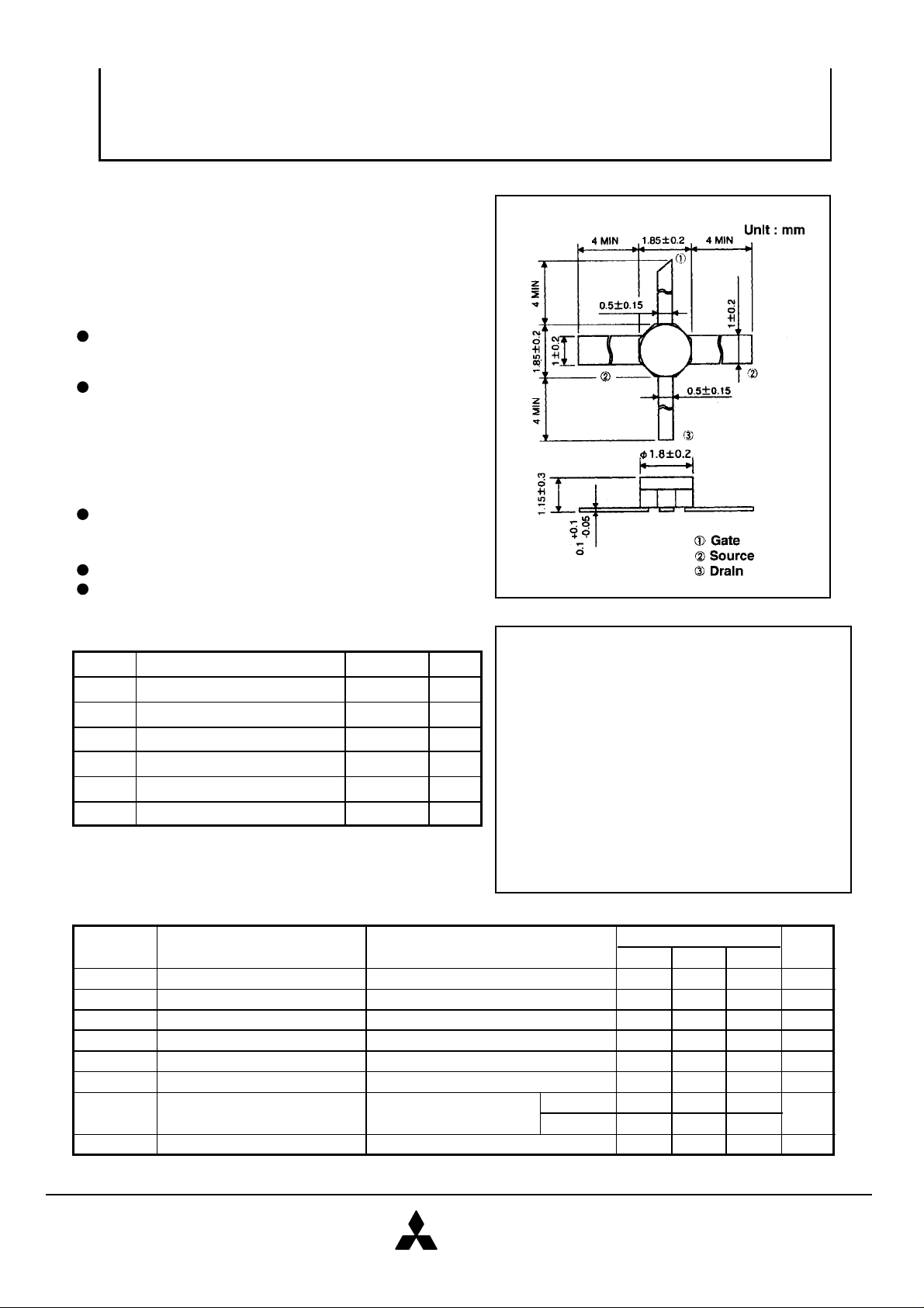
OUTLINE DRAWING
GD-4
< Keep safety first in your circuit designs! >
Mitsubishi Electric Corporation puts the maximum effort into
V
making semiconductor products better and more reliable,
but there is always the possibility that trouble may occur
with them.Trouble with semiconductors may lead to personal
injury, fire or property damage. Remember to give due
consideration to safety when making your circuit designs,
with appropriate measures such as (i)placement of
substitutive, auxiliary circuits, (ii)use of non-flammable
material or (iii)prevention against any malfunction or mishap.
ELECTRICAL CHARACTERISTICS
Symbol Parameter Test conditions
IGSS
VGS (off)
gm
Gs Associated gain 13.5
NFmin Minimum noise figure
*1 : Channel to ambient
Gate to source leakage current
Saturated drain currentIDSS
Gate to Source cut-off voltage
Transconductance
( Ta=25°C )
Min. Typ. Max
IG= -10µA —-3Gate to drain breakdown voltageV(BR)GDO —
VGS= -2V, VDS=0V
VGS=0V, VDS=2V
VDS=2V, ID=500µA
VDS=2V, ID=10mA —
VDS=2V, ID=10mA, f=12GHz 12
VDS=2V, ID=10mA, f=12GHz
*1
MGF4316G
MGF4319G
—
MITSUBISHI
ELECTRIC
Limits
—
—
75 mS—
——
Unit
50 µA
6015
-1.5—-0.1
—
0.8
0.5——
mA
dB
dB
˚C/W—— 625Rth (ch-a) ∆Vf methodThermal resistance
as of Apr.'98
V
V
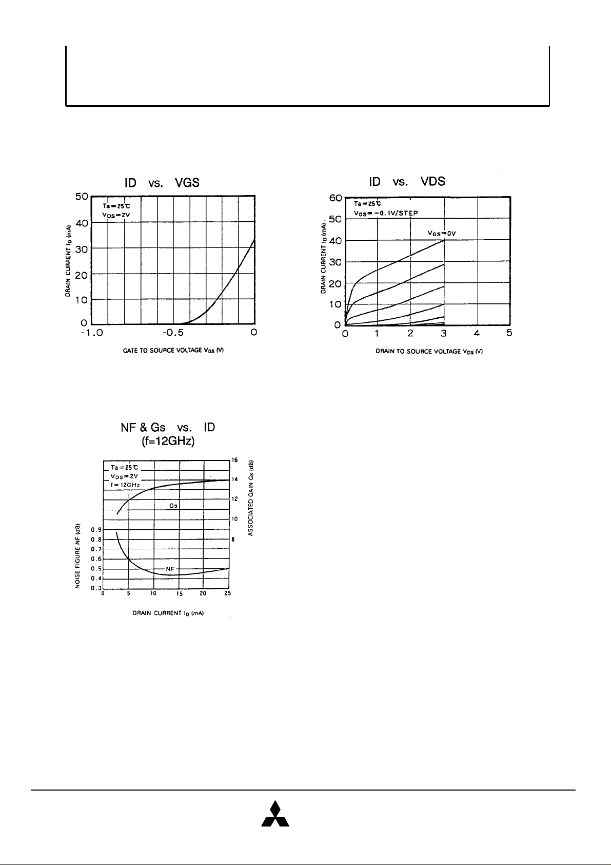
Typical Characteristics
MITSUBISHI SEMICONDUCTOR <GaAs FET>
MGF431xG
Super Low Noise InGaAs HEMT
MITSUBISHI
ELECTRIC
as of Apr.'98

MITSUBISHI SEMICONDUCTOR <GaAs FET>
MGF431xG
Super Low Noise InGaAs HEMT
Typical Characteristics
S Parameters (Ta=25˚C , VDS=2V , ID=10mA )
f S11 S21 S12 S22 MSG/MAG K
(GHz) Magn. Angle Magn. Angle Magn. Angle Magn. Angle (dB)
1 0.990 -22.3 5.775 158.1 0.020 71.9 0.533 -19.2 28.8 0.10
2 0.967 -40.6 5.585 140.6 0.035 61.8 0.514 -33.4 26.5 0.19
3 0.925 -53.2 5.401 128.9 0.051 53.3 0.489 -42.9 24.3 0.27
4 0.874 -70.9 5.161 111.8 0.064 42.4 0.457 -58.2 21.6 0.35
5 0.831 -88.8 4.899 96.8 0.075 29.3 0.424 -71.6 19.8 0.43
6 0.783 -105.7 4.626 80.8 0.083 19.0 0.391 -87.5 18.1 0.50
7 0.743 -120.6 4.316 67.9 0.087 9.1 0.369 -100.6 16.8 0.57
8 0.706 -132.1 4.100 56.4 0.090 4.1 0.357 -110.8 15.9 0.64
9 0.682 -144.7 3.887 43.2 0.093 -6.4 0.357 -122.3 15.1 0.69
10 0.670 -159.1 3.765 30.1 0.094 -14.3 0.351 -133.0 14.7 0.72
11 0.639 -171.8 3.617 17.5 0.095 -24.4 0.339 -143.5 14.0 0.80
12 0.617 175.3 3.526 4.5 0.096 -33.5 0.329 -154.0 13.5 0.86
13 0.591 163.1 3.421 -8.1 0.094 -42.5 0.328 -163.9 13.0 0.91
14 0.571 152.9 3.349 -17.4 0.094 -50.9 0.328 -171.3 12.7 0.95
15 0.565 140.1 3.333 -29.6 0.096 -61.1 0.343 179.5 12.7 0.96
16 0.560 125.8 3.349 -44.4 0.098 -74.1 0.351 170.5 12.7 0.98
17 0.533 109.8 3.356 -59.9 0.101 -88.8 0.337 161.8 12.5 1.01
18 0.484 91.2 3.337 -77.0 0.104 -105.1 0.310 151.6 12.1 1.11
Noise Parameters (Ta=25˚C , VDS=2V , ID=10mA )
f
(GHz)
4 0.76 49 12.5 0.31 18.3
8 0.59 95 4.7 0.47 15.9
12 0.48 139 2.3 0.60 13.5
14 0.41 166 1.8 0.69 12.3
18 0.34 -142 1.5 0.88 9.9
G opt.
Magn. Angle
Rn
(Ω)
NFmin.(dB)
MGF4316G MGF4319G
0.24
0.35
0.45
0.50
0.61
MITSUBISHI
ELECTRIC
Gs
(dB)
as of Apr.'98
 Loading...