

Page 1
MITSUBISHI Proprietary
< Power GaAs FET >
MGF1953A
Leadless ceramic package
DESCRIPTION
The MGF1953A power MES FET is designed for use in S to Ku band
power amplifiers.
The lead-less ceramic package assures minimum parasitic losses.
FEATURES
High gain and High P1dB
Glp=6.0dB , P1dB=20dBm (Typ.) @ f=12GHz
APPLICATION
S to Ku band low noise amplifiers
QUALITY GRADE
GG
RECOMMENDED BIAS CONDITIONS
VDS=4V , ID=100mA
Not to be reproduced or disclosed without
permission by Mitsubishi Electric
ORDERING INFORMATION
Tape & reel 3,000pcs/reel
RoHS COMPLIANT
MGF1953A is a RoHS compliant product. RoHS compliance is indicated by the letter “G” after the Lot Marking.
ABSOLUTE MAXIMUM RATINGS
Symbol Parameter Ratings Unit
V
GDO
V
GSO
ID
PT Total power dissipation 1 W
Tch
T
stg
Gate to drain voltage -8 V
Gate to source voltage -8 V
Drain current 400 mA
Channel temperature 125 °C
Storage temperature -65 to +125 °C
(Ta=25°C )
ELECTRICAL CHARACTERISTICS
Symbol
V
(BR)GDO
I
V
GS(off)
P1dB Output power at 1dB gain
Glp Linear power gain
Note: P1B and Glp are tested with sampling inspection.
Gate to drain breakdown voltage
Saturated drain current
DSS
Gate to source cut-off voltage
compression
Parameter Test conditions
IG=-100µA
VGS=0V,VDS=3V
VDS=3V,ID=1mA
(Ta=25°C )
VDS=4V, ID=100mA,
f=12GHz
VDS=4V, ID=100mA,
f=12GHz, Pin=-5dBm
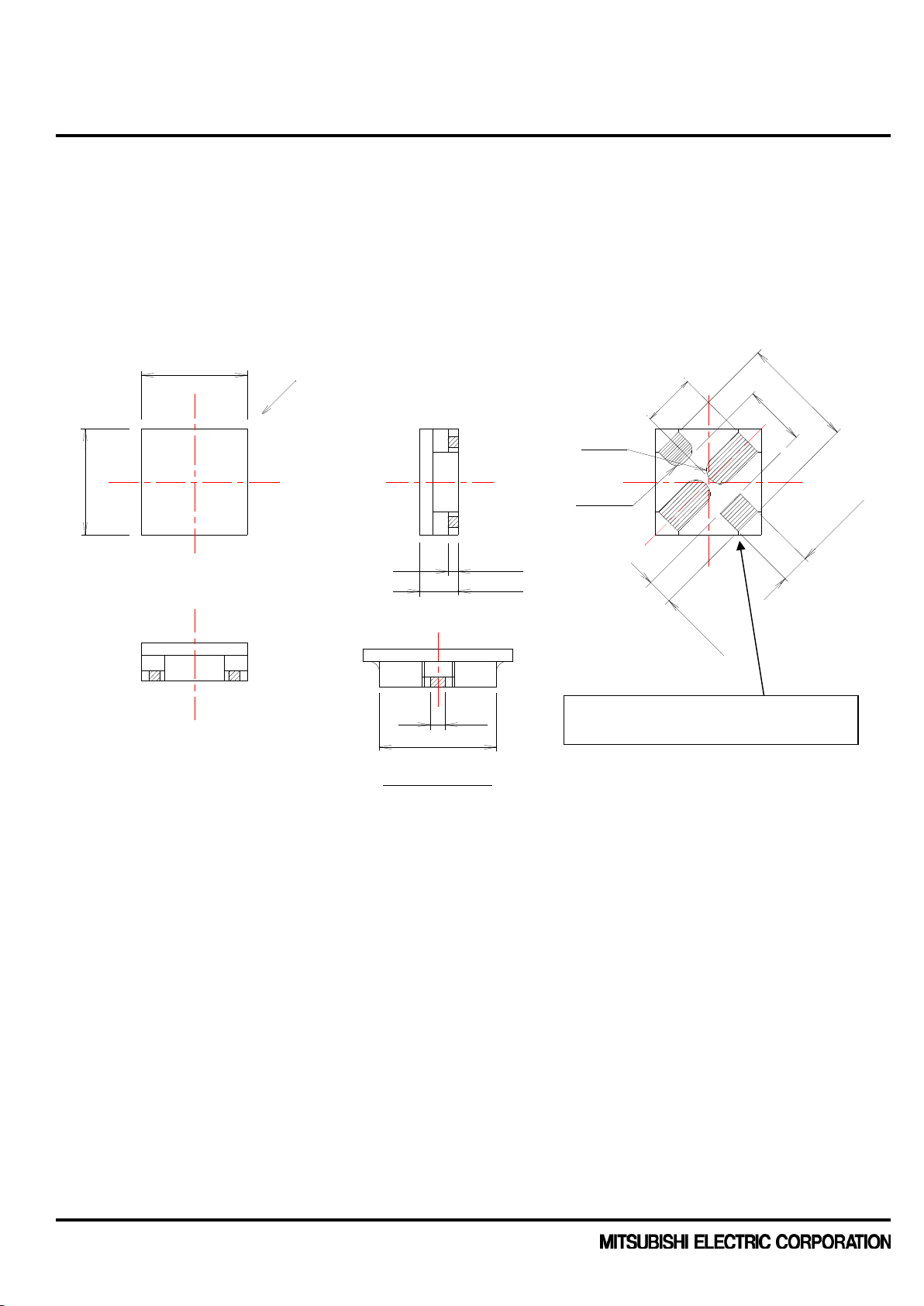
Outline Drawing
Fig.1
Limits Unit
MIN. TYP. MAX
-8 -15 -- V
105 200 400 mA
-0.3 -1.4 -3.5 V
18 20 -- dBm
4 6 -- dB
Publication Date : Apr., 2011
1
Page 2
< Power GaAs FET >
ℵ
ℑ
ℵ
ℑ
E
2
4 A A
MGF1953A
Leadless ceramic package
Fig.1
Top
+0.20
-0.102.15
A
②
①
0
0
2
1
.
.
0
0
+
-
5
1
.
2
③
②
Side
0.20±0.1
0.80±0.1
2-R0.275
2-R0.20
①
②
Bottom
)
2
0
.
1
(
-
2
2
-
0
2
-
(
2
②
.
2
1
0
.
)
2
0
±
0
.
0
5
5
0
.
③
.
5
0
±
0
.
0
5
0
±
5
5
.
0
-
4
(0.30)
(2.30)
from "A" side view
Square shape electrode is Drain
Unit: mm
① Gate
② Source
③ Drain
Publication Date : Apr., 2011
2
Page 3

< Power GaAs FET >
MGF1953A
Leadless ceramic package
TYPICAL CHARACTERISTICS
300
250
200
Ta=25deg.C
VGS=-0.2V/STEP
ID vs. V
150
100
DRAIN CURRENT ID(mA)
50
0
0.0 1.0 2.0 3.0 4.0 5.0 6.0 7.0 8.0 9.0 10.0
DRAIN TO SOURCE VOLTAGE VDS(V)
Po vs. Pin
Po vs. Pin
Po vs. PinPo vs. Pin
30
30
3030
25
25
2525
20
20
2020
Ta= 2 5 d e g.C
Ta= 2 5 d e g.C
Ta= 2 5 d e g.CTa= 2 5 d e g.C
VD S = 4 V
VD S = 4 V
VD S = 4 VVD S = 4 V
ID= 10 0 m A
ID= 10 0 m A
ID= 10 0 m AID= 10 0 m A
f= 1 2GH z
f= 1 2GH z
f= 1 2GH zf= 1 2GH z
15
15
1515
Po (dBm )
Po (dBm )
Po (dBm )
Po (dBm )
10
10
1010
5555
0000 5555 10
DS
VGS=0V
10 15
1010
Pin (d Bm)
Pin (d Bm)
Pin (d Bm)Pin (d Bm)
15 20
1515
(Ta=25°C)
20 25
2020
25
2525
300
Ta=25deg.C
VDS=4V
250
(mA)
D
200
I
150
100
DRAIN CURRENT
50
0
-3.0 -2.5 -2.0 -1.5 -1.0 -0.5 0.0
GATE TO SOURCE VOLTAGE VGS(V)
ID vs. V
GS
Publication Date : Apr., 2011
3
Page 4

< Power GaAs FET >
MGF1953A
Leadless ceramic package
S PARAMETERS
f S11 S21 S12 S22 K
(GHz) Mag. Angle Mag. Angle Mag. Angle Mag. Angle (dB)
1 0.907 -51.1 8.288 143.0 0.026 63.3 0.148 -62.0 0.40 25.0
2 0.775 -95.1 6.461 112.7 0.041 42.5 0.161 -105.9 0.73 21.9
3 0.702 -121.5 5.090 95.3 0.049 34.4 0.173 -123.3 0.99 20.1
4 0.674 -144.5 4.128 79.9 0.055 28.9 0.187 -138.9 1.16 16.3
5 0.661 -161.3 3.521 66.9 0.060 23.7 0.190 -145.1 1.29 14.5
6 0.653 -175.4 3.105 54.6 0.065 20.8 0.185 -146.9 1.38 13.1
7 0.650 170.8 2.810 41.7 0.071 17.5 0.175 -147.3 1.41 12.2
8 0.650 157.4 2.609 28.9 0.078 12.7 0.164 -149.1 1.40 11.5
9 0.642 143.3 2.440 16.2 0.086 6.9 0.142 -154.0 1.40 10.8
10 0.640 127.4 2.270 2.4 0.096 -0.1 0.114 -165.1 1.39 10.0
11 0.623 109.0 2.091 -12.5 0.103 -10.3 0.083 166.0 1.50 8.9
12 0.619 90.0 1.908 -27.6 0.106 -20.4 0.085 113.6 1.63 7.9
13 0.634 71.7 1.710 -42.4 0.108 -29.8 0.140 75.8 1.75 7.0
14 0.666 54.3 1.507 -57.2 0.107 -41.2 0.217 54.5 1.86 6.2
15 0.713 39.4 1.314 -70.2 0.105 -50.7 0.300 41.8 1.89 5.5
16 0.769 27.0 1.139 -82.8 0.101 -59.9 0.378 32.0 1.84 5.2
17 0.822 15.6 0.976 -95.2 0.097 -68.4 0.455 23.4 1.76 5.0
18 0.865 5.9 0.821 -107.2 0.091 -77.2 0.513 15.3 1.67 4.7
Reference Point
(Conditions : VDS=4V,ID=100mA,Ta=25deg.C)
Gate
Source
Source
Reference Point
Drain
Note
We are ready to provide nonlinear model for ADS and MWO users. If you are interested, please contact our
sales offices.
Publication Date : Apr., 2011
4
Page 5

< Power GaAs FET >
MGF1953A
Leadless ceramic package
• Mitsubishi Electric Corporation puts the maximum effort into making semiconductor products better and
more reliable, but there is always the possibility that trouble may occur with them. Trouble with
semiconductors may lead to personal injury, fire ore property damage. Remember to give due
consideration to safety when making your circuit designs, with appropriate measures such as (i) placement
of substitutive, auxiliary circuits, (ii) use of non-flammable material or (iii) prevention against any
malfunction or mishap.
• These materials are intended as a reference to assist our customers in the selection of the Mitsubishi
semiconductor product best suited to the customer’s application; they do not convey any license under any
intellectual property rights, or any other rights, belonging to Mitsubishi Electric Corporation or a third party.
• Mitsubishi Electric Corporation assumes no responsibility for any damage, or infringement of any thirdparty’s rights, originating in the use of any product data, diagrams, charts, programs, algorithms, or circuit
application examples contained in these materials.
• All information contained in these materials, including product data, diagrams, charts, programs and
algorithms represents information on products at the time of publication of these materials, and are subject
to change by Mitsubishi Electric Corporation without notice due to product improvements or other reasons.
It is therefore recommended that customers contact Mitsubishi Electric Corporation or an authorized
Mitsubishi Semiconductor product distributor for the latest product information before purchasing a product
listed herein.
The information described here may contain technical in accuracies or typographical errors.
Mitsubishi Electric Corporation assumes no responsibility for any damage, liability, or other loss rising from
these inaccuracies or errors.
Please also pay attention to information published by Mitsubishi Electric Corporation by various means,
including the Mitsubishi Semiconductor home page (http://www.mitsubishielectric.com/).
• When using any or all of the information contained in these materials, including product data, diagrams,
charts, programs, and algorithms, please be sure to evaluate all information as a total system before
making a final decision on the applicability of the information and products. Mitsubishi Electric Corporation
assumes no responsibility for any damage, liability or other loss resulting from the information contained
herein.
• Mitsubishi Electric Corporation semiconductors are not designed or manufactured for use in a device or
system that is used under circumstances in which human life is potentially at stake. Please contact
Mitsubishi Electric Corporation or an authorized Mitsubishi Semiconductor product distributor when
considering the use of a product contained herein for any specific purposes, such as apparatus or systems
for transportation, vehicular, medical, aerospace, nuclear, or undersea repeater use.
• The prior written approval of Mitsubishi Electric Corporation is necessary to reprint or reproduce in whole
ore in part these materials.
• If these products or technologies are subject to the Japanese export control restrictions, they must be
exported under a license from the Japanese government and cannot be imported into a country other than
the approved destination.
Any diversion or re-export contrary to the export control laws and regulations of Japan and/or the country
of destination is prohibited.
• Please contact Mitsubishi Electric Corporation or an authorized Mitsubishi Semiconductor product
distributor for further details on these materials or the products contained therein.
© 2011 MITSUBISHI ELECTRIC CORPORATION. ALL RIGHTS RESERVED.
Keep safety first in your circuit designs!
Notes regarding these materials
Publication Date : Apr., 2011
5
 Loading...