

Mitsubishi MF-622DF-T12-430, MF-622DS-R13-242, MF-622DS-R13-241, MF-622DF-T12-462, MF-622DF-T12-460 Datasheet
...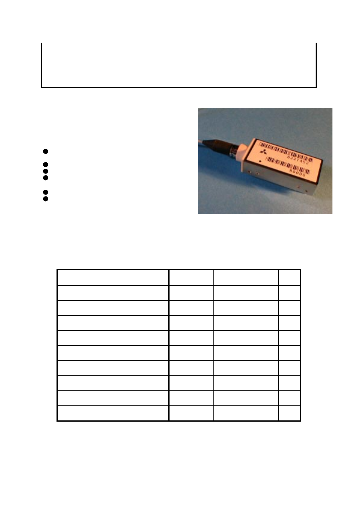
MITSUBISHI (OPTICAL DEVICES)
MF-622DF-T12-43x/45x/46x
MF-622DS-R13-24x
SONET/SDH TRANSMITTER & RECEIVER
DESCRIPTION
Transmitter uses uncooled laser in a hermetic pigtail
coaxial module with drivered by specific integrated
circuit.
Receiver uses PIN preamp in a hermetic pigtail
coaxial module and integrated circuits for reshaping,
retiming and regenerating optical signal.
FEATURES
SONET,SDH system from intra-office to longleach application fully line up
Low cost and Low power consumption
Multisourced 20-Pin DIP with pigtail fiber
Single +5V power supply and P-ECL compatible
input and output
Operating case temperature range -40 to 85°C.
With clock recovery and digital alarm function
APPLICATION
Short haul and long haul telecommunication systems
for SDH STM-4 / SONET OC-12.
ABSOLUTE MAXIMUM RATINGS
Stress below listed absolute maximum rating may cause permanent damage to the module.
This is a stress only and functional operation of the module at these or any other conditions in excess of those
given in the operational sections of this data sheet.
Exposure to Absolute Maximum Rating for extended periods may affect module reliability.
Ta=25°C
Parameters Symbol Ratings Unit
Supply voltage Vcc +6 to 0 V
PECL high output current - -50 to 0 mA
PECL input voltage - 0 to Vcc+0.4 V
Storage temperature Tstg -40 to 85
Operating case temperature Tc -40 to 85
Soldering Temperature - +260
Soldering Time - 10 sec
Relative humidity(non condensation) - 10 to 80 %
Fiber bend radius from package rF 32 mm
C
°
C
°
C
°
MITSUBISHI (OPTICAL DEVICES)
MF-622DS-T12-43x/45x/46x
MF-622DS-R13-24x
SONET/SDH TRANSMITTER & RECEIVER
ELECTRICAL CHARACTERISTICS
All parameters are specified over the operating case temperature.
Measurement conditions are at 622.08Mb/s+/-20ppm, NRZ PN2
The DATA input/output and CLOCK output signal levels are PECL compatible.
The transmitter disable input signal level is CMOS/TTL compatible.
The Signal Detect output signal level is PECL level compatible.
Transmitter
Parameters Condition Symbol Min. Typ. Max. Unit
Supply voltage - Vcc 4.75 5.0 5.25 V
Power consumption - Pc - 0.75 1.5 W
PECL input voltage note 1 - PECL -
Transmitter Disable voltage note 2 Vd Vcc-2.0V - Vcc V
23
-1 and 50%duty cycle data signal.
Transmitter Enable voltage note 2 Ve 0 - 0.8 V
Laser bias monitor voltage note 3 Vb 0.01 - 0.70 V
Laser backface monitor voltage note 3 Vbf 0.01 - 0.20 V
Receiver
Parameters Condition Symbol Min. Typ. Max. Unit
Supply voltage Vcc 4.75 5.0 5.25 V
Power consumption Pc - 1.2 1.5 W
PECL input voltage note 4,5 - PECL -
Data/Clock external Load note 4 RI 50 ohm
Data to clock phase note 6 Tcda -200 - 200 psec.
Clock duty note 6 - 45 - 55 %
Jitter - ITU Rec.compliant -
Signal Detect Response Time:
Decreasing Light Input
Signal Detect Response Time:
Increasing Light Input
Photo Bias Current Responsity note 8 PBr 0.6 - - A/W
note 5,7 SDRTd - - 100 us
note 5,7 SDRTi - - 100 us
OPTICAL CHARACTERISTICS
Parameter Specification Unit
ITU code S-4.1 L-4.1 L-4.2
Optical Budget 0 17 10 28.5 10 29 dB
Transmitter
Wavelength 1274 1356 1280 1335 1480 1580 nm
Optical source MLM SLM SLM Optical power at pigtail -14 -8 -2.5 +2 -2 +2 dBm
Optical power when disable - -45 - -45 - -45 dBm
Spectral width(rms) - 2.5 - - - - nm
Spectral width(-20dB) - - - 1 - 1 nm
MITSUBISHI (OPTICAL DEVICES)
MF-622DS-T12-43x/45x/46x
MF-622DS-R13-24x
SONET/SDH TRANSMITTER & RECEIVER
Min. Max. Min. Max. Min. Max.
SMSR - - 30 - 30 - dB
Extinction ratio 8.2 - 10 - 10 - dB
Optical wave form SONET/SDH Mask compliant -
Path penalty
(dispersion=ITU-T compliant)
Receiver
Wavelength 1260 1580 nm
Sensitivity - -33 -31 dBm
Overload -8 -3 - dBm
ORDERING INFORMATION
Transmitter
Part number ITU-code Optical connector type
MF-622DF-T12-430 S-4.1 FC
MF-622DF-T12-431 S-4.1 SC
MF-622DF-T12-432 S-4.1 ST
MF-622DF-T12-450 L-4.1 FC
MF-622DF-T12-451 L-4.1 SC
MF-622DF-T12-452 L-4.1 ST
MF-622DF-T12-460 L-4.2 FC
MF-622DF-T12-461 L-4.2 SC
MF-622DF-T12-462 L-4.2 ST
Receiver
Part number ITU-code Optical connector type
MF-622DS-R13-240 STM-4 FC
MF-622DS-R13-241 STM-4 SC
MF-622DS-R13-242 STM-4 ST
-1-1-1dB
Min. Typ. Max.

MITSUBISHI (OPTICAL DEVICES)
MF-622DS-T12-43x/45x/46x
MF-622DS-R13-24x
SONET/SDH TRANSMITTER & RECEIVER
TRANSMITTER PIN ALLOCATION
No. Symbol Description No. Symbol Description
1 NC No user connection 20 NC No user connection
2 Lbs(+) Laser-bias monitor(+) 19 Lbf(+) Laser-backface monitor(+)
3 NC No user connection 18 Vcc Vcc
4 Lbs(-) Laser-bias monitor(-) 17 Lbf(-) Laser-backface monitor(-)
5 GND Ground 16 Data Data
6 Vcc Vcc 15 Data Data
7 Td Transmitter disable 14 GND Ground
8 Vcc Vcc 13 GND Ground
9 Vcc Vcc 12 Vcc Vcc
10 NC No user connection 11 GND Ground
PIN DESCRIPTIONS
Pin No. Function I/O Pin description
5,11,
13,14
6,8,9,
12,18
15,16 Data & Data I This data input pin modulates the laser diode. When th e Data input is asser ted, the
7 Transmitter disable I The transmitter is nomally enabled and only requires an external voltage to disable.
2,4 Laser-bias
17,19 Laser-backface
1,3,
10,20
GND I These pin are the module’s ground connections.
Vcc I This is the power supply pin for the module.
monitor(+),
Laser-bias monitor(-)
monitor(+),
Laser-backface
monitor(-)
NC - These pin are No user connection and should be left open.
They should be connected to a low impedance ground plane (0V).
It should be connected to +5.0V.
Recommended power supply decoupling.
laser diode is turned on.
Si g nal l e v el of th es e pi n are PEC L le vel a nd i nte rn al Vb b bi as. Re f er t o e le c tr i c al
interface in NOTE1.
Refer to electrical interface in NOTE2.
O The laser bias current is calculated as a ratio of the voltage to an internal 10-ohm
sensing resistor.
Ib[mA]={Lbs(+)-Lbs(-)}[mV]/10
Refer to electrical interface in NOTE3.
O Th e laser b ackface monit or is calculated as a rati o of the volt age to an i nternal 200-
ohm sensing resistor.
Ibf[mA]={Lbf(+)-Lbf(-)}[mV]/200
Refer to electrical interface in NOTE3.

MITSUBISHI (OPTICAL DEVICES)
MF-622DS-T12-43x/45x/46x
MF-622DS-R13-24x
SONET/SDH TRANSMITTER & RECEIVER
RECEIVER PIN ALLOCATION
No. Symbol Description No. Symbol Description
1 GND Ground 20 NC No user connection
2 GND Ground 19 NC No user connection
3 GND Ground 18 NC No user connection
4 CLK Clock 17 NC No user connection
5 CLK Clock 16 GND Ground
6 GND Ground 15 GND Ground
7 Data Data 14 SD Signal Detect
8 GND Ground 13 GND Ground
9 Data Data 12 SD Signal Detect
10 PDB Photo Detector Bias 11 Vcc Vcc
RECEIVER PIN DESCRIPTIONS
Pin No. Function I/O Pin description
1,2,3,
6,8,13,
15,16
11 Vcc I This is the power supply pin for the module.
7,9 Data & Data O There are Data output pin (Differential PECL output).
4,5 Clock & Clock O There are recovered clock output pin (Differential PECL output).
12,14 Signal Detect
10 Photo Detector Bias I This pin supplies th e bias for the PIN Photo Detector and it should be connecte d to
17,18,
19,20
GND I These pin are the module’s ground connections.
&
Signal Detect
NC - These pin are No user connection and should be left open.
They should be connected to a low impedance ground plane (0V).
It should be connected to +5.0V.
Recommended power supply decoupling.
Signal level of these pin are PECL level.
Refer to electrical interface in NOTE4.
Signal level of these pin are PECL level.
Refer to electrical interface in NOTE4.
O When the optical input signal fall bellow the SD threshold level, The Signal Detect
is deasserted and its output logic level changes form a PECL HIGH to PECL LOW.
Signal Detect pin is differential PECL output pin.
Refer to electrical interface in NOTE5.
+5.0V.
Ad dition ally, by usin g Exter nal Resi sto r in seri es with this pin, it is po ssible to
measure the photocurrent.
Refer to electrical interface in NOTE8.

MITSUBISHI (OPTICAL DEVICES)
MF-622DS-T12-43x/45x/46x
MF-622DS-R13-24x
SONET/SDH TRANSMITTER & RECEIVER
GENERAL OUTLINE DRAWING
Transmitter / Receiver (FC/PC, SC/PC and ST/PC connector are available)
NOTE: TOLERANCES UNLESS NOTED +/-0.5
DIMENSIONS ARE IN MILLIMETERS
L=900+/-100

BLOCK DIAGRAM
DRIVER IC
MF-622DS-T12-43x/45x/46x
LD Module
MITSUBISHI (OPTICAL DEVICES)
MF-622DS-R13-24x
SONET/SDH TRANSMITTER & RECEIVER
PD LD
Integrated device
OPT.OUT
DATA IN
DATA IN
OPT.IN
Driver
IC
A.P.C.
Curcuit
Transmitter Block Diagram
PD
Preamp
Rt
Amp
Laser-backface
monitor(+)
Laser-backface
monitor(-)
Laser-bias monitor(+)
Laser-bias monitor(-)
Transmitter disable
Clock recovery ICLimiting IC
DATA Out
Decider
DATA Out
CLK Out
CLK Out
PD-Preamp
Module
Receiver Block Diagram
Alarm
PLL
Signal Detect

NOTE
NOTE1: PECL Input Interface
MITSUBISHI (OPTICAL DEVICES)
MF-622DS-T12-43x/45x/46x
MF-622DS-R13-24x
SONET/SDH TRANSMITTER & RECEIVER
13Kohm
Data
PECL
NOTE2: Transmitter disable Interface
Td
HCMOS
51Kohm
Data
comparator
Transmitter
47Kohm
Transmitter
Disable Input
Optical Output
ON
Vcc
0V
OFF
The transmitter is normally enabled and only requires an external voltage to disable.

MF-622DS-T12-43x/45x/46x
NOTE3: Laser bias / Laser backface monitor Interface.
MITSUBISHI (OPTICAL DEVICES)
MF-622DS-R13-24x
SONET/SDH TRANSMITTER & RECEIVER
Transmitter
NOTE4: PECL Output interface
DC-coupled AC-coupled
Receiver
200ohm
A.P.C.
Curcuit
PD LD
3Kohm
3Kohm
LD
Module
3Kohm
10ohm
3Kohm
Receiver
Laser backface
current monitor
Laser bias
current monitor
Data / Clock
Data / Clock
50ohm
Vcc-2V
NOTE5: Signal Detect Interface
330ohm
Receiver
330ohm
50ohm
PECL
0.1uF
Signal Detect
Signal Detect
PECL
Data / Clock
Data / Clock
330ohm
Optical Signal
Signal Detect
Signal Detect
0.1uF
0.1uF
330ohm
OFF ON
50ohm

NOTE6: Data and Clock relationship
Data
MITSUBISHI (OPTICAL DEVICES)
MF-622DS-T12-43x/45x/46x
MF-622DS-R13-24x
SONET/SDH TRANSMITTER & RECEIVER
Clock
Td
Td < +/-200psec.
NOTE7: Signal Detect Response time: Decreasing Light Input / Increasing Light Input
Optical wave Optical wave
SDRTiSDRTd
NOTE8: Photo current monitor method
Vcc
External resister
(R=<100ohm)
Photo Detector Bias Receiver
45% < Clock duty < 55%
SDRTd < 100usec.
SDRTi < 100usec.
PD
OPT.IN
Preamp
Rt
PD-Preamp Module
The photocurrent will be calculated based on the voltage drop across on external resistor connected between the
monitoring pin and +5V.
 Loading...