

Mitsubishi MF365A-LCDATXX, MF3513-LSDATXX, MF34M1-LSDATXX, MF34M1-LCDATXX, MF3129-LCDATXX Datasheet
...
MITSUBISHI MEMORY CARD
STATIC RAM CARDS
8/16-bit Data Bus
Static RAM Card
Connector Type
Two- piece 68-pin
DESCRIPTION
Mitsubishi’s Static RAM cards provide large
memory capacities on a device approximately the
size of a credit card(85.6mm×54mm×3.3mm).
The cards use a 8/16 bit data bus.The devices
use a replaceable lithium battery to maintain data.
Available in 64K byte-4M byte capacities,
Mitsubishi’s Static RAM cards are available with
a 68-pin, two-piece connector.
MF365A-LCDATXX
MF365A-LSDATXX
MF3129-LCDATXX
MF3129-LSDATXX
MF3257-LCDATXX
MF3257-LSDATXX
MF3513-LCDATXX
MF3513-LSDATXX
MF31M1-LCDATXX
MF31M1-LSDATXX
MF32M1-LCDATXX
MF32M1-LSDATXX
MF34M1-LCDATXX
MF34M1-LSDATXX
Electrostatic discharge protectiton to 15kV
Buffered interface
68-pin connector
8-bit and 16-bit data width
Write protect switch
Battery voltage pin
LS Type Wide Range operating temperature
Ta= -20 to 70°C
FEATURES
Uses TSOP (Thin Small Outline Package) to
achieve very high memory density coupled
with high reliability, without enlarging card
size
PRODUCT LIST
Item Memory Data Bus Attribute Auxialiary Memory Outline Main battery
Type name capacity width(bits) memory battery organization drawing holder
MF365A-LCDATXX 64KB 256K bit SRAM×2
MF3129-LCDATXX 128KB 256K bit SRAM×4
MF3257-LCDATXX 256KB 1M bit SRAM×2
MF3513-LCDATXX 512KB 1M bit SRAM×4
MF31M1-LCDATXX 1MB 1M bit SRAM×8
MF32M1-LCDATXX 2MB 1M bit SRAM×16
MF34M1-LCDATXX 4MB 8/16 NO NO 4M bit SRAM×8 68P-003 Screw type
MF365A-LSDATXX 64KB 256K bit SRAM×2
MF3129-LSDATXX 128KB 256K bit SRAM×4
MF3257-LSDATXX 256KB 1M bit SRAM×2
MF3513-LSDATXX 512KB 1M bit SRAM×4
MF31M1-LSDATXX 1MB 1M bit SRAM×8
MF32M1-LSDATXX 2MB 1M bit SRAM×16
MF34M1-LSDATXX 4MB 4M bit SRAM×8
APPLICATIONS
Office automation Data Communications
Computers Industrial
Telecommunications Consumer
MITSUBISHI
ELECTRIC
1/11
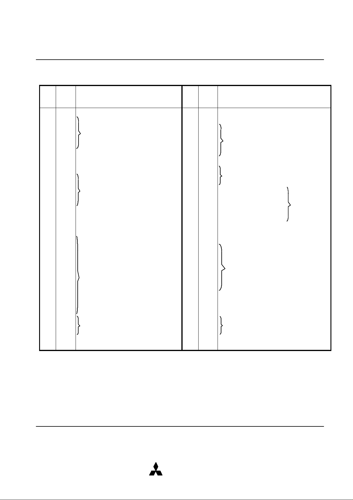
PIN ASSIGNMENT
1
GND
Ground
35
GND
Ground
2D336
CD1#
Card detect 1
3D437
D114D5
Data I/O
38
D125D639D13
Data I/O
6D740
D147CE1#
Card enable 1
41
D158A10
Address input
42
CE2#
Card enable 2
9
OE#
Output enable
43NC10
A1144NC
No connection
11A945NC12A8 Address input
46
A17
A17(NC for≤128KB types)
13
A1347A18
A18(NC for≤256KB types)
14
A1448A19
A19(NC for≤512KB types)
15
WE#
Write enable
49
A20
A20(NC for≤1MB types)
16NCNo connection
50
A21
A21(NC for≤2MB types)
17
VCCPower supply voltage
51
VCCPower supply voltage
18NCNo connection
52NCNo connection
19
A16
A16(NC for 64KB type)
53NCNo connection
20
A1554NC21A1255NC22A756NC23A657NC
No connection
24A5 Address input
58NC25A459NC26A360NC27A261
REG#
REG function
28A162
BVD2
Battery voltage detect 2
29A063
BVD1
Battery voltage detect 1
30D064D831D1 Data I/O
65D9 Data I/O
32D266
D1033WP
Write protect
67
CD2#
Card detect 2
34
GND
Ground
68
GND
Ground
Two-Piece Type (68-pin)
MITSUBISHI MEMORY CARD
STATIC RAM CARDS
Pin Pin
Symbol
No. No.
Function
Symbol
Function
Address input
WRITE PROTECT MODE (WP)
When the write protect switch is switched on, this
card goes into a write protect mode that can read
but not write data.
In this mode, the WP pin becomes “H” level.
At the shipment the write protect switch is switched
off (Normal mode : The card can be written ; WP pin
indicates “L” level).
MITSUBISHI
ELECTRIC
2/11
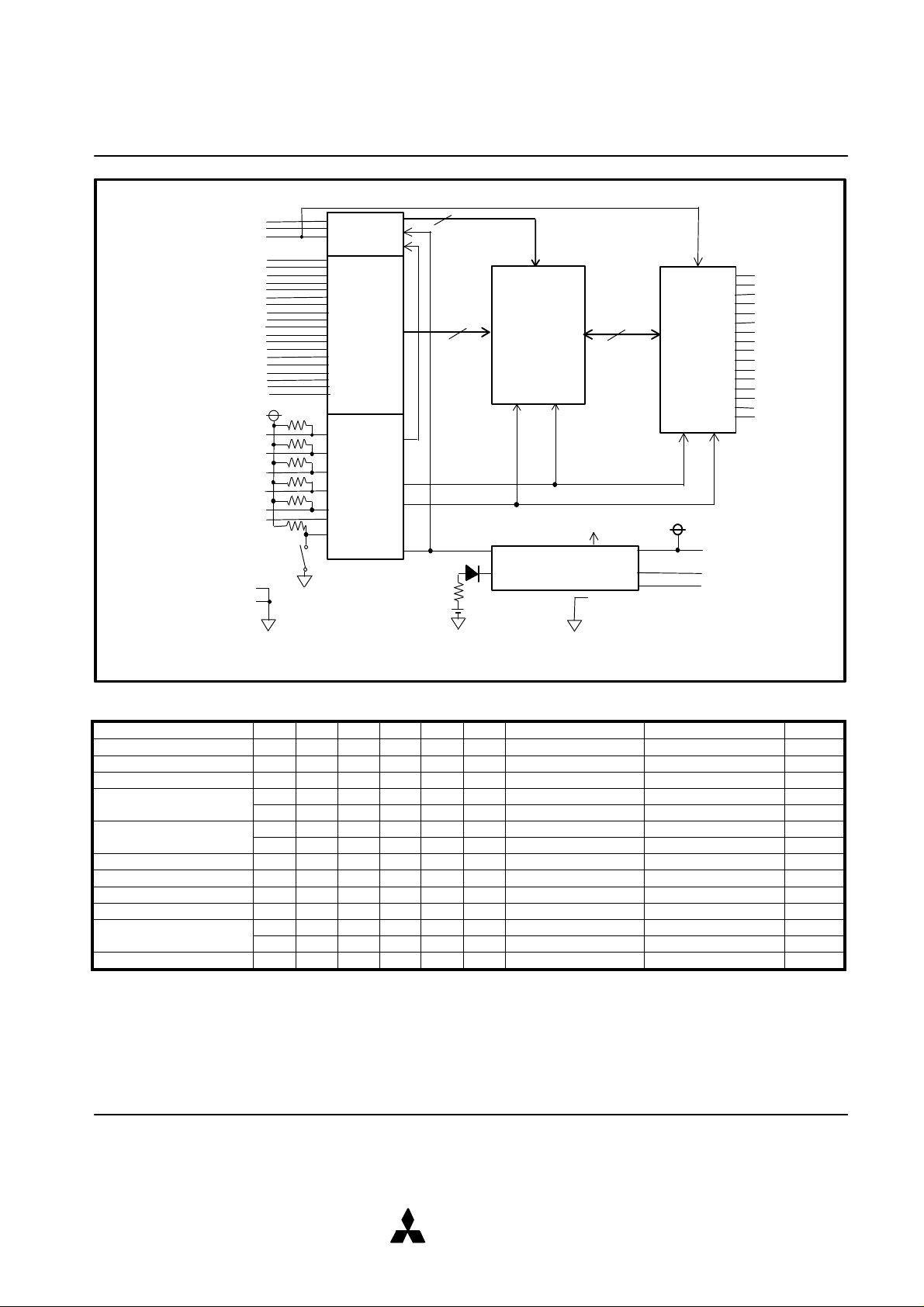
BLOCK DIAGRAM (4MB)
A21
D0
BVD1
WP#
WRITE PROTECT
ON
19
16
BR2325
POWER CONTROLLER
POWER
8
MITSUBISHI MEMORY CARD
STATIC RAM CARDS
CE1#
CE2#
WE#
OE#
REG#
CD1#
CD2#
A20
A0
A19
A18
A17
A16
A15
A14
A13
A12
A11
A10
A9
A8
A7
A6
A5
A4
A3
A2
A1
OFF
ADDRESSDECODER
ADDRESS-
BUS
BUFFERS
MODE
CONTROL
LOGIC
CS#
COMMON
MEMORY
4Mbit SRAM×8
OE# WE#
TO INTERNAL
VOLTAGE DETECTOR
&
GND
DATA-BUS
BUFFERS
VCC
BVD2
D15
D14
D13
D12
D11
D10
D9
D8
D7
D6
D5
D4
D3
D2
D1
FUNCTION TABLE
Mode
REG# CE1# CE2# OE# WE# A0
Standby X H H X X X High-impedance High-impedance Standby
Read A (16bit) common H L L L H X Odd Byte Data out Even Byte Data out Active
Write A (16bit) common H L L H L X Odd Byte Data in Even Byte Data in Active
Read B (8bit) common H L H L H L High-impedance Even Byte Data out Active
H L H L H H High-impedance Odd Byte Data out Active
Write B (8bit) common H L H H L L High-impedance Even Byte Data in Active
H L H H L H High-impedance Odd Byte Data in Active
Read C (8bit) common H H L L H X Odd Byte Data out High-impedance Active
Write C (8bit) common H H L H L X Odd Byte Data in High-impedance Active
Output disable X X X H H X High-impedance High-impedance Active
Read A (16bit) attribute L L L L H X Data out (unknown) Data out (FFh) Active
Read B (8bit) attribute L L H L H L High-impedance Data out (FFh) Active
L L H L H H High-impedance Data out (unknown) Active
Read C (8bit) attribute L H L L H X Data out (unknown) High-impedance Active
I/O (D15~D8) I/O (D7~D0) ICC
Note 1 : H=VIH, L=VIL, X=VIH or VIL
MITSUBISHI
ELECTRIC
3/11
MITSUBISHI MEMORY CARD
STATIC RAM CARDS
ABSOLUTE MAXIMUM RATINGS
Symbol Parameter Conditions Ratings Unit
VCC Supply voltage -0.3~6.0 V
Vi Input voltage With respect to GND -0.3~VCC+0.3 V
Vo Output voltage 0~VCC V
Topr1 Operating temperature 1 Read, Write, Operation LC series 0~70 °C
LS series -20~70 °C
Topr2 Operating temperature 2 Data retention LC series 0~70 °C
LS series -20~70 °C
Tstg Storage temperature -30~80 °C
RECOMMENDED OPERATING CONDITIONS (LC series Ta= 0~55°C, unless otherwise noted)
(LS series Ta=-20~70°C, unless otherwise noted)
Symbol
VCC VCC Supply voltage 4.50 5.0 5.25 V
GND System ground 0 V
VIH High input voltage 3.5 VCC V
VIL Low input voltage 0 0.8 V
Parameter
Min. Typ. Max.
Limits
Unit
MITSUBISHI
ELECTRIC
4/11

MITSUBISHI MEMORY CARD
STATIC RAM CARDS
ELECTRICAL CHARACTERISTICS (LC series Ta= 0~55°C, VCC=4.50~5.25V, unless otherwise noted)
(LS series Ta=-20~70°C, VCC=4.50~5.25V, unless otherwise noted)
Symbol
VOH High output voltage IOH=-1.0mA 2.4 V
VOL Low output voltage IOL=1mA 0.4 V
IIH High input current VI=VCC V 10 µA
IIL Low input current VI=0V CE1#, CE2#, WE#, OE#, REG# -10 -70 µA
IOZH High output current CE1#=CE2#=VIH or OE#=VIH WE#=VIH, 10 µA
IOZL Low output current CE1#=CE2#=VIH or OE#=VIH WE#=VIH, -10 µA
ICC 1 • 1 Active supply Other inputs VIH or VIL 2MB 16bit 160 mA
ICC 1 • 2 Active supply Other inputs ≤0.2V or 2MB 16bit 150 mA
ICC 2 • 1 Standby supply current 1 CE1#=CE2#=VIH
ICC 2 • 2 Standby supply current 2 Other inputs ≤ 0.2V or 256KB~1MB 0.15 0.45 mA
VBDET1 Battery detect Vcc=5V,Ta=25°C V
VBDET2 Battery detect Vcc=5V,Ta=25°C V
Parameter
in off state VO=VCC
in off state VO=0V
CE1#=CE2#=VIL 8bit 110
current 1 Outputs=open 8bit 120
Cycle time=250ns 4MB 16bit 200
CE1#=CE2# ≤ 0.2V 8bit 100
current 2 ≥ VCC-0.2V 8bit 110
Outputs=open 4MB 16bit 190
Cycle time=250ns 8bit 150
Other inputs=VIH or VIL
CE1#=CE2# ≥ VCC-0.2V 64KB,128KB 0.15 0.30
≥ VCC-0.2V 2MB,4MB 0.30 0.65
reference voltage 1
reference voltage 2
¬
¬
Test conditions Unit
Other inputs -10
64KB~1MB 16bit 150
8bit 160
64KB~1MB 16bit 140
Note 2 : Currents flowing into the IC are taken as positive (unsigned).
3 : Typical values are measured at VCC=5V, Ta=25°C.
¬
Pin asserted when battery voltage drops below specified level.
Limits
Min. Typ. Max.
10 mA
2.37
2.65
2.47
2.75
2.27
2.55
MITSUBISHI
ELECTRIC
5/11

MITSUBISHI MEMORY CARD
STATIC RAM CARDS
CAPACITANCE
Symbol
CI Input capacitance VI=GND, VI=25mVrms 64KB~2MB 45 pF
CO Output capacitance VO=GND, VO=25mVrms, 64KB~2MB 45 pF
Note 4 : These parameters are not 100% tested.
SWITCHING CHARACTERISTICS
Read Cycle (LC series Ta= 0~55°C, VCC=4.50~5.25V, unless otherwise noted)
(LS series Ta=-20~70°C, VCC=4.50~5.25V, unless otherwise noted)
Parameter
f=1 MHZ, Ta=25°C 4MB 30
f=1 MHZ, Ta=25°C 4MB 20
Symbol Parameter
tCR Read cycle time 200 ns
ta(A) Address access time 200 ns
ta(CE) Card enable access time 200 ns
ta(OE) Output enable accese time 100 ns
tdis(CE) Output disable time (from CE#) 90 ns
tdis(OE) Output disable time (from OE#) 90 ns
ten(CE) Output enable time (from CE#) 5 ns
ten(OE) Output enable time (from OE#) 5 ns
tV(A) Data valid time (after address change) 0 ns
Test conditions
Min. Typ. Max.
Limits
Min. Typ. Max.
Limits
Unit
Unit
TIMING REQUIREMENTS
Write Cycle(LC series Ta= 0~55°C, VCC=4.50~5.25V, unless otherwise noted)
(LS series Ta=-20~70°C, VCC=4.50~5.25V, unless otherwise noted)
Limits
Symbol Parameter
tCW Write cycle time 200 ns
tw(WE) Write pulse width 120 ns
tsu(A) Address set up time 20 ns
tsu(A-WEH) Address set up time with respect to WE# high 140 ns
tsu(CE-WEH) Card enable set up time with respect to WE# high 140 ns
tsu(D-WEH) Data set up time with respect to WE# high 60 ns
th(D) Data hold time 30 ns
trec(WE) Write recovery time 30 ns
tdis(WE) Output disable time (from WE#) 90 ns
tdis(OE) Output disable time (from OE#) 90 ns
ten(WE) Output enable time (from WE#) 5 ns
ten(OE) Output enable time (from OE#) 5 ns
tsu(OE-WE) OE# set up time with respect to WE# low 10 ns
th(OE-WE) OE# hold time with respect to WE# high 10 ns
Min. Typ. Max.
Unit
MITSUBISHI
ELECTRIC
6/11

MITSUBISHI MEMORY CARD
t
ta(A)
ta
ten
ten(OE)
tdis
t
ta(OE)
OUTPUT VALID
Hi-Z
t
Hi-Z
ten(OE)
t
tSU(CE-WEH)
tSU(A-WEH)
tSU(A)
th
tW(WE)
tSU(OE-WE)
tdis(OE)
tdis(WE)
trec(WE)
ten(WE)
Hi-Z
STATIC RAM CARDS
TIMING DIAGRAM
Read Cycle
An
VIH
VIL
VIH
CE#
VIL
VIH
OE#
VIL
Dm
(DOUT)
Write Cycle (WE# control)
VOH
VOL
WE#=“H” level
REG#=“H” level
CR
V(A)
(CE)
(CE)
Note 5 : Indicates the don’t care input
CW
dis(CE)
(OE)
An
CE#
OE#
WE#
Dm
(DIN)
Dm
(DOUT)
VIH
VIL
VIH
VIL
VIH
VIL
VIH
VIL
VIH
VIL
VOH
VOL
REG#=“H” level
tSU(D-WEH)
DATA INPUT STABLE
th(D)
(OE-WE)
MITSUBISHI
ELECTRIC
7/11

Write Cycle (CE# control)
tCRR
Read cycle time
300nsta(A)R
Address access time
300nsta(CE)R
Card enable access time
300nsta(OE)R
Output enable access time
150nstdis(CE)R
Output disable time (from CE#)
100nstdis(OE)R
Output disable time (from OE#)
100nsten(CE)R
Output enable time (from CE#)
5nsten(OE)R
Output enable time (from OE#)
5nstV(A)R
Data valid time after address change
0
ns
tCWt
tSU(A)
trec(WE)
Hi-Z
VIH
An
VIL
VIH
CE#
VIL
VIH
WE#
VIL
Dm
(DIN)
VIH
VIL
MITSUBISHI MEMORY CARD
SU(CE-WEH)
tSU(D-WEH)
DATA INPUT STABLE
STATIC RAM CARDS
th(D)
OE#=“H” level
REG#=“H” level
SWITCHING CHARACTERISTICS (Attribute)
Read Cycle(LC series Ta= 0~55°C, VCC=4.50~5.25V, unless otherwise noted)
(LS series Ta=-20~70°C, VCC=4.50~5.25V, unless otherwise noted)
Limits
Symbol Parameter Min. Typ. Max. Unit
MITSUBISHI
ELECTRIC
8/11

TIMING DIAGRAM (Attribute)
tCRR
ta(A)R
ta
R
ten
R
ten
R
tdis
R
t
R
ta(OE)R
OUTPUT VALID
Hi-Z
tdis(CE)R
Read Cycle
VIH
An
VIL
VIH
CE#
VIL
VIH
OE#
VIL
Dm
(DOUT)
VOH
VOL
(CE)
(CE)
(OE)
MITSUBISHI MEMORY CARD
STATIC RAM CARDS
V(A)
(OE)
WE#=“H” level
REG#=“L” level
Note 6 : Test Conditions
Input pulse levels : VIL=0.4V, VIH=4.0V
Input pulse rise, fall time : tr=tf=10ns
Reference voltage
Input : VIL=0.8V, VIH=3.5V
Output : VOL=0.8V, VOH=3.0V
(ten and tdis are measured when output voltage is± 500mV from steady state. )
Load : 100pF+1 TTL gate
5pF+1 TTL gate (at ten and tdis measuring)
7 : Writing is executed in overlap of CE# and WE# are “L” level. (only for Common Memory)
8 : Don’t apply inverted phase signal externally when Dm pin is in output mode.
9 : CE# is indicated as follows:
Read A/Write A : CE#=CE1#=CE2#
Read B/Write B : CE#=CE1#, CE2#=“H” level
Read C/Write C : CE#=CE2#, CE1#=“H” level
MITSUBISHI
ELECTRIC
9/11

MITSUBISHI MEMORY CARD
STATIC RAM CARDS
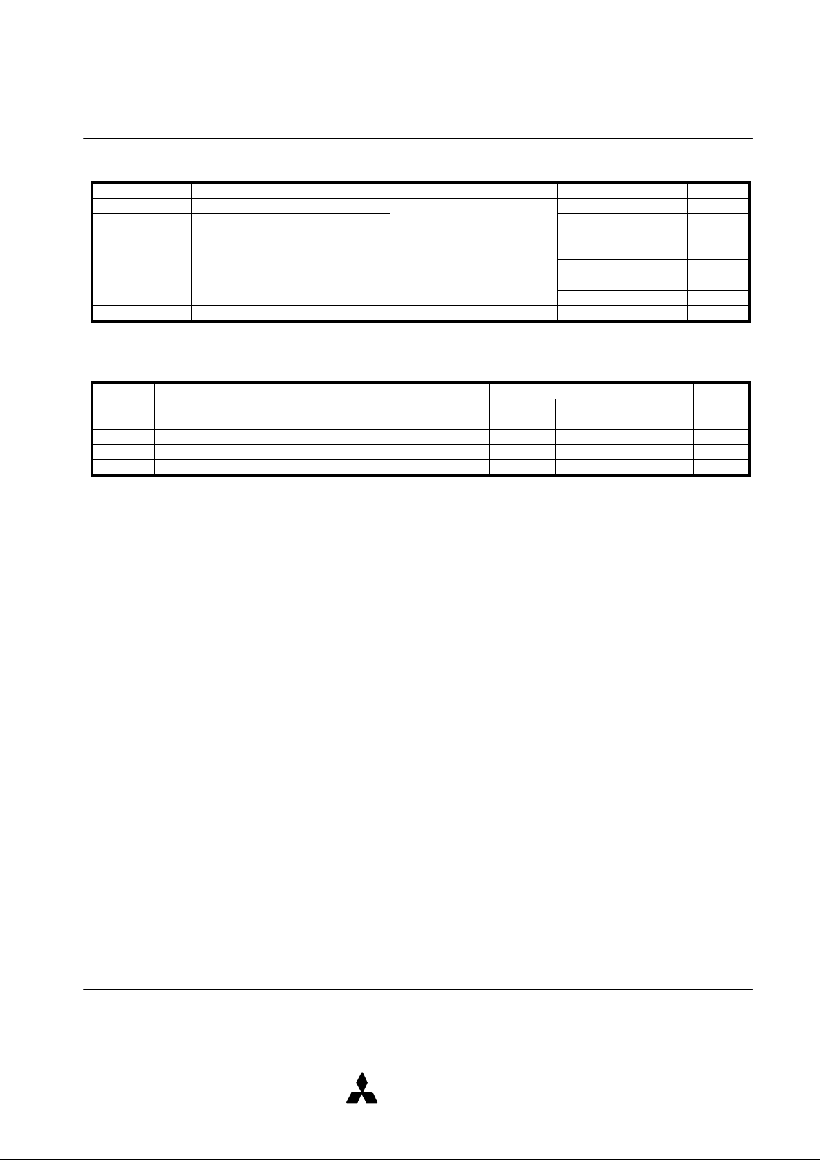
ELECTRICAL CHARACTERISTICS
BATTERY BACKUP (LC series Ta= 0~55°C, unless otherwise noted)
(LS series Ta=-20~70°C, unless otherwise noted)
Limits
Symbol Parameter Test Conditions Min. Typ. Max. Unit
VBATT Back-up enable battery voltage All pins open 2.6 V
VI(CE) Card enable voltage 2.4V≤VCC≤5.25V 2.4 V
0V≤VCC<2.4V VCC-0.1 VCC VCC+0.1
64KB 3
128KB 5
All pins open, 256KB 3
ICC(BUP) Battery back-up supply current VBATT=3V, 512KB 5 µA
Ta=25°C 1MB 9
2MB 17
4MB 9
64KB 40
128KB 70
256KB 100
ICC(BUP) Battery back-up supply current All pins open, 512KB 200 µA
VBATT=3V 1MB 400
2MB 800
4MB 400
TIMING REQUIREMENTS (LC series Ta= 0~55°C, unless otherwise noted)
(LS series Ta=-20~70°C, unless otherwise noted)
Limits
Symbol Parameter Min. Typ. Max. Unit
tpr Power supply rise time 0.1 300 ms
tpf Power supply fall time 3 300 ms
tsu(VCC) Set up time at power on 20 ms
trec(VCC) Recovery time at power off 1000 ns
MITSUBISHI
ELECTRIC
10/11

MITSUBISHI MEMORY CARD
CE2#
90%
CE2
STATIC RAM CARDS
CARD INSERTION/REMOVAL TIMING DIAGRAM
VCC MIN means Minimum Operating Voltage=4.75V.
90%
tpf
VIH
10%
10%
VCC
VCC MIN
trec(VCC)
CE1#,
Note 10: When the card is holding valuable data, the battery must not be removed unless VCC is
present.
BATTERY SPECIFICATIONS
A replaceable battery (type BR2325) with a capacity of 165mAH is used:
Estimated battery life when the card is left continuously.
MF365A-LC/LSDATXX 5.9years
MF3129-LC/LSDATXX 3.6years
MF3257-LC/LSDATXX 5.9years
MF3513-LC/LSDATXX 3.6years
MF31M1-LC/LSDATXX 2.0years
MF32M1-LC/LSDATXX 1.1years
MF34M1-LC/LSDATXX 2.0years
Conditions
Temperature : 25°C
Humidity : 60%RH
VIH
tpr
VCC MIN
tsu(VCC)
VCC
CE1,
MITSUBISHI
ELECTRIC
11/11
 Loading...