

Mitsubishi MF-2500DS-T12-211, MF-2500DS-T12-191, MF-2500DS-T12-200, MF-2500DS-T12-201, MF-2500DS-T12-190 Datasheet
...
MITSUBISHI (OPTICAL DEVICES)
MF-2500DS-T12-18x/19x/20x/21x
MF-2500DS-R13-18x
MF-2500DS-R14-19x/20x/21x
SONET/SDH TRANSMITTER & RECIEVER
DESCRIPTION
This product is designed to provide high optical
performance for SDH STM-16/SONET OC-48.
Transmitter uses uncooled laser module with drivered
by specific integrated circuit.
Receiver uses PD or APD preamp-module and
integrated circuits for reshaping, retiming and
regenerating optical signal.
2.5Gb/s ATM LAN and ATM switching systems.
FEATURES
Full SONET/SDH line up
Low cost
Compact, low power
-5.2V,+5V power supply, DC/DC converter built in
for Rx
Case Temp. Range: Class 1; -5 to +75°C / Class
2; -40 to +85°C
Clock recovery
Multi source
APPLICATION
Short haul and long haul telecommunication systems
for SDH STM-16 / SONET OC-48.
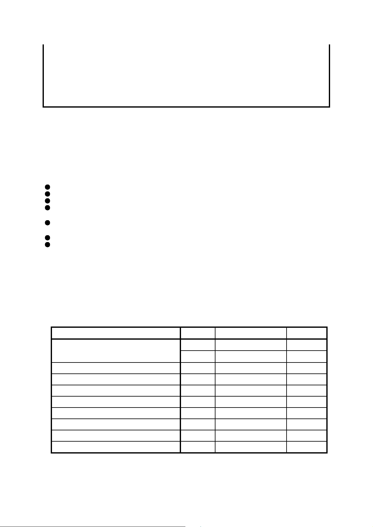
ABSOLUTE MAXIMUM RATINGS
Stress below listed absolute maximum rating may cause permanent damage to the module.
This is a stress o nly and f unctional operat ion of t he m odule at t hese or any ot her c onditions in excess of t hose
given in the operational sections of this data sheet .
Exposure to Absolute Maximum Rating for extended periods may affect module reliability.
Tc=25°C
Parameters Symbol Ratings Unit
Vcc +6.0 V
Supply voltage
High output current - TBD mA
Input voltage - TBD V
Storage temperature Tstg -40 to +85
Operating case temperature Tc
Soldering Temperature - +260
Soldering Time - 10 sec
Relative humidity(non condensation) - 10 to 80 %
Fiber bend radius - 32 mm
Vee -6.0 V
class 1:-5 to +75
class 2:-40 to +85
°C
°C
°C
MITSUBISHI (OPTICAL DEVICES)
MF-2500DS-T12-18x/19x/20x/21x
MF-2500DS-R13-18x
MF-2500DS-R14-19x/20x/21x
SONET/SDH TRANSMITTER & RECIEVER
ELECTRICAL/OPTICAL CHARACTERISTICS
All parameters are specified over the operating case temperature.
Measurement conditions are at 2488.32Mb/s +/-20ppm, NRZ PN223-1 and 50% duty cycle data signal.
Vcc=+5.0V+/-5%, Vee=-5.2V+/-5%, and for Transmitter.
note : Vcc-Vee ; with Vcc at +5V Vee must be at 0V ; with Vee at -5.5V Vcc must be at 0V
note : Internally AC coupled with 50ohm internal termination
(TLD=25°C, unless otherwise noted)
Transmitter
class1 : -5°C to +75°C class2 : -40°C to +85°C
Parameters Condition Symbol Min. Typ. Max. Unit
Supply voltage note 1 - 4.75 5.0 5.5 V
Power consumption total - - 0.8 2.0 W
Input sensitivity data and clock voltage note 2,3 SV 0.6 0.8 1.0 Vpp
Normalized back face voltage note 5 - - 500 - mV
Monitor bias voltage note 5 - - 20 - mV/mA
Logic level note 4 - TTL compatible -
note 1: Vcc-Vee ; with Vcc at +5V Vee must be at 0V ; with Vee at -5.5V Vcc must be at 0V
note 2: Internally AC coupled with 50ohm internal termination
note 3: This sensitivity is achieved by applying at minimum either a 0.6Vpp signal on one input while
the other input is tied to ground or by applying two complementary 0.3Vpp signal on both inputs.
note 4: when Vcc at +5V and Vee at 0V
note 5: This voltage is measured taking Vee as reference.
Receiver
class1 : -5°C to +75°C class2 : -40°C to +85°C
Parameters Condition Symbol Min. Typ. Max. Unit
Positive supply voltage - 4.75 5.0 5.25 V
Negative supply voltage if equired - -5.5 -5.2 -4.94 V
Power consumption total - - 1.3 3 W
Output data and clock voltage single ended SV 0.3 0.4 1 Vpp
Output data and clock voltage differential DV 0.6 0.8 2 Vpp
Jitter generation GR-253/ITU-T G958 Ulrms
Jitter tolerance GR-253/ITU-T G958 Ulpp
Jitter transfer peaking - GR-253/ITU dB
Logic output level note 6 - TTL compatible -
note 6: At the moment the jitter bandwidth performance according GR-253/ITU-T G958 is not met atthe receiver interface level.
Additional clock filtering is supposed to be done at lower data rates.
Jitter transfer bandwidth will be defined at this level which is a parameter of the whole network element and not of the
receiver element.
A further version is under investigation to met simultaneously all the GR-253/ITU-T G958 jitter specifications at the
physical interface level.
MITSUBISHI (OPTICAL DEVICES)
nom
sen
ovr
nom
sen
ovr
MF-2500DS-T12-18x/19x/20x/21x
MF-2500DS-R13-18x
MF-2500DS-R14-19x/20x/21x
SONET/SDH TRANSMITTER & RECIEVER
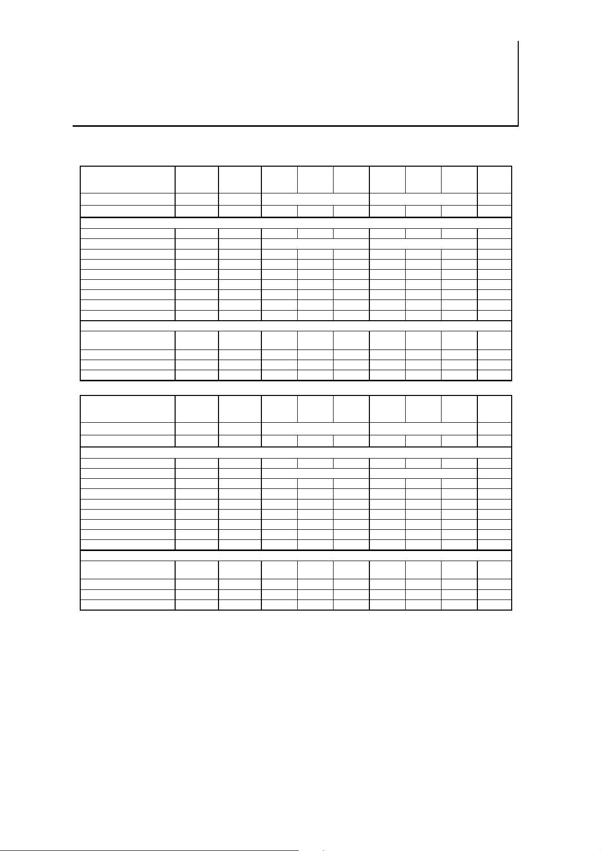
OPTICAL CHARACTERISTICS
cond. symb. Min. Typ. Max. Min Typ. Max
ITU-T/SONET - - S-16.1/IR-1 L-16.1/LR-1 Optical budget note7 - 0 - 12 10 - 24 dB
Transmitter
Center wavelength - - 1270 1310 1360 1280 1310 1335 nm
Optical source - - SLM SLM Optical output power note8 S
Shutdown optical power - Sidle - -50 -40 - -50 -40 dBm
Spectral width note9 - - 0.3 1 - 0.3 1 nm
SMSR - - 30 - - 30 - - dB
Extinction ratio note10 ER 8.2 - - 8.2 - - dB
Dispersion - - 100 - - 250 - - ps/nm
maximum return loss - - - - 24 - - 24 dB
Receiver
Receiver sensitivity
Receiver overload note13 R
Path penalty - - - 0.2 1 - 0.2 1 dB
Maximum reflectance - - - - -27 - - -27 dB
note11
note12
R
-4.5 -2 0 -1.5 0 +3 dBm
- -20.5 -18.5 - -29.5 -27.5 dBm
0 +1 - -8 -7 - dBm
cond. Symb. Min. Typ. Max. Min Typ. Max
ITU-T/SONET - - L-16.1/LR-2 V-16.2 Optical budget note7 - 10 - 24 22 - 33 dB
Transmitter
Center wavelength - - 1500 1530 1580 1530 1545 1565 nm
Optical source - - SLM SLM Optical output power note8 S
Shutdown optical power - Sidle - -50 -40 - -50 -40 dBm
Spectral width note9 - - 0.3 1 - 0.3 0.8 nm
SMSR - - 30 - - 30 - - dB
Extinction ratio note10 ER 8.2 - - 8.2 - - dB
Dispersion - - 1600 - - 2400 - - ps/nm
maximum return loss - - - - 24 - - 24 dB
Receiver
Receiver sensitivity
Receiver overload note13 R
Path penalty - - - 1.3 2 - 1.5 2 dB
Maximum reflectance - - - - -27 - - -27 dB
note7:The V-16.2 version is adapted to standard 10dBm to 13dBm EDFA optical bandwidth.
note8:Measured at the connector interface. Provision of 0.5dB is taken for S point measurement.
note9:The maximum full width of the central wavelength peak, measured 20dB down from maximum amplitude
under modulation condition PRBS 223-1.
note10:Measured at the connector interface under modulation condition PRBS 223-1.
note11:Measured at BER 10
note12:Provision of 0.5dB is taken for R point measurement if SMF fiber is used.
Note13:The device must not be damaged when this optical power is applied to the optical input.
The device is not meant to operate at such an optical input power.
All min and max. parameters are specified End-of-Life within the overall relevant operating temperature range.
The typical values are referenced to +25deg.C ,nominal power supply, beginning of life.
-10
note11
note12
.
R
-1.5 0 +3 -4.5 0 +3 dBm
- -30.5 -28.5 - -27.5 -25.5 dBm
-8 -7 - -9 -8 - dBm

ORDERING INFORMATION
Transmitter
Part number ITU-code Optical connector type
MF-2500DS-T12-180 S-16.1 FC
MF-2500DS-T12-181 S-16.1 SC
MF-2500DS-T12-190 L-16.1 FC
MF-2500DS-T12-191 L-16.1 SC
MF-2500DS-T12-200 L-16.2 FC
MF-2500DS-T12-201 L-16.2 SC
MF-2500DS-T12-210 V-16.2 FC
MF-2500DS-T12-211 V-16.2 SC
Receiver
Part number ITU-code Optical connector type
MF-2500DS-R13-180 S-16.1 FC
MF-2500DS-R13-181 S-16.1 SC
MF-2500DS-R14-190 L-16.1 FC
MF-2500DS-R14-191 L-16.1 SC
MF-2500DS-R14-200 L-16.2 FC
MF-2500DS-R14-201 L-16.2 SC
MF-2500DS-R14-210 V-16.2 FC
MF-2500DS-R14-211 V-16.2 SC
MITSUBISHI (OPTICAL DEVICES)
MF-2500DS-T12-18x/19x/20x/21x
MF-2500DS-R13-18x
MF-2500DS-R14-19x/20x/21x
SONET/SDH TRANSMITTER & RECIEVER

MITSUBISHI (OPTICAL DEVICES)
MF-2500DS-T12-18x/19x/20x/21x
MF-2500DS-R13-18x
MF-2500DS-R14-19x/20x/21x
SONET/SDH TRANSMITTER & RECIEVER
PIN ALLOCATION
Transmitter pin allocation
No. Symbol Description No. Symbol Description
1 VEE Negative power supply **** 24 VCC Positive power supply ****
2 BACK(+) Monitoring for back fact current 23 GND Ground
3 BIAS(+) Monitoring for LD current 22 Cki- False clock input
4 SDC Shut Down Command *** 21 GND Ground
5 SELC Clock mode select ** 20 Cki+ True clock input *
6 GND Ground 19 GND Ground
7 NUC No user connection 18 Di- False data input
8 LDA Laser Degrade Alarm ***** 17 GND Ground
9 NUC No user connection 16 Di+ True data input
10 NUC No user connection 15 GND Ground
11 GND Ground 14 NUC No user connection
12 VEE Negative power supply **** 13 VCC Positive power supply ****
*: The falling edge of Cki clock input signal is at the Di data eye pattern crossing point.
**: When open (or low) the module is in the operating mode. When high the module operates in non
clocked mode.
***: When high the module in the shut down mode (no optical output power).
When open (or low) the module is in the operating mode.
****: Vcc-Vee; with Vcc at +5V Vee must be at 0V; with Vee at -5.5V Vcc must be at 0V
*****: When provided a digital alarm indicates that the laser is degraded.
The active level is a low level.
This pin must be teidto Vcc through a 100k ohm resistor when the digital alarm is not proved
Receiver pin allocation
No. Symbol Description No. Symbol Description
1 HV / NIC High Voltage * 24 NUC No user connection
2 NUC No user connection 23 OILV / NIC Optical Input Light Voltage ##
3 LPA Loss of Power Alarm *** 22 VCC Positive power supply
4 GND Ground ** 21 NUC No user connection
5 Cko- False clock output 20 GND Ground **
6 Cko+ True clock output 19 GND Ground **
7 GND Ground ** 18 VEE Negative power supply
8 VCC Positive power supply 17 GND Ground **
9 GND Ground 16 GND Ground **
10 Do+ True data output 15 GND Ground **
11 Do- False data output 14 GND Ground **
12 GND Ground ** 13 DTV / NIC Decision Threshold Voltage #
*: This pin is Not Internally Connected(NIC) in case of the high voltage generator is inside the module.
**: Package is at same potential as GND .
***: LPA output is a logic level that indicates the presence or absence of a sufficient optical input level.
A logical high level indicates an input optical level too low.
#: This pen is not internally connected if the amplitude decision threshold is not made adjustable.
##: This pen is not internally connected if the Optical Input Light Voltage functionality is not provided.

GENERAL OUTLINE DRAWING
Transmitter
MITSUBISHI (OPTICAL DEVICES)
MF-2500DS-T12-18x/19x/20x/21x
MF-2500DS-R13-18x
MF-2500DS-R14-19x/20x/21x
SONET/SDH TRANSMITTER & RECIEVER
NOTE:TOLERANCES UNLESS NOTED +/-0.5
DIMENSIONS ARE IN MILLIMETERS
Receiver

BLOCK DIAGRAM
MITSUBISHI (OPTICAL DEVICES)
MF-2500DS-T12-18x/19x/20x/21x
MF-2500DS-R13-18x
MF-2500DS-R14-19x/20x/21x
SONET/SDH TRANSMITTER & RECIEVER
SELC
DATAin
DATAin
CLOCKin
CLOCKin
: integrated device
DRIVER IC
Driver IC
Modulation
Control
DC/DC APD Control
LD Module
APC IC
VCC
PD
A.P.C
Transmitter
VCC
LD
OPT. OUT
Monitoring for back
face current
Monitoring for LD current
Laser Degrade Alarm
SDC
: in case of APD version
OPT. IN
APD/PD
Preamp
APD/PD-Preamp Module
Amp
Alarm
AGC Amp
Receiver
DATAout
DATAout
Decider
CLKout
CLKout
PLL
Clock recovery IC
Signal Detect

NOTE
NOTE1: Input interface
MITSUBISHI (OPTICAL DEVICES)
MF-2500DS-T12-18x/19x/20x/21x
MF-2500DS-R13-18x
MF-2500DS-R14-19x/20x/21x
SONET/SDH TRANSMITTER & RECIEVER
Data
Data
AC Coupled Interface
NOTE2: Shut Down Command interface
Signal detect
TTL
Td
H
L
VBB
Transmitter
Transmitter
50ohm
Optical signal
OFF
ON
The transmitter is normally enabled and only requires
an external voltage to disable.
NOTE3: Laser bias / Laser backface monitor interface
LD Module
A.P.C
comparator
Laser backface
current monitor
Laser bias
current monitor

NOTE4: Output interface
MITSUBISHI (OPTICAL DEVICES)
MF-2500DS-T12-18x/19x/20x/21x
MF-2500DS-R13-18x
MF-2500DS-R14-19x/20x/21x
SONET/SDH TRANSMITTER & RECIEVER
LVPECL
Data / Clock
Receiver
NOTE5: Data and Clock relationship
NOTE6: Signal detect interface
Receiver
Data / Clock
TBD
Optical signal
Signal detect
Signal detect
ON
50ohm
OFF
H
L
TTL
 Loading...