

Mitsubishi MF0060M-03AT, MF0045M-03AT, MF007M5-03AT, MF0090M-03AT, MF0075M-03AT Datasheet
...
MITSUBISHI STORAGE CARD
ATA PC CARDS
MITSUBISHI
ELECTRIC
1 1997.Nov. Rev. 1.2
8/16-bit Data Bus
Flash ATA PC Card
Connector Type
Two- piece 68-pin
DESCRIPTION
Mitsubishi’s Flash ATA cards provide large
memory capacities on a device approximately
the size of a credit card
(85.6mm×54mm×3.3mm). The cards use a 8/16
bit data bus.
Available in 7.5MB, 15MB, 30MB, 45MB,
60MB, 75MB, 90MB and 105MB capacities,
Mitsubishi’s Flash ATA cards conform to the
JEIDA/PCMCIA standard.
In default mode, the ATA card operates in PC
Card compliant sockets. It conforms to
PCMCIA2.1, JEIDA4.2 and PC Card Standard.
When the OE# signal is asserted low level by
the Host system in power on cycle, the
Mitsubishi’s Flash ATA cards can be selected
in a IDE ATA interface. It uses the ATA
command set so no software drivers are
required.
MF007M5-03ATxx
MF0015M-03ATxx
MF0030M-03ATxx
MF0045M-03ATxx
MF0060M-03ATxx
MF0075M-03ATxx
MF0090M-03ATxx
MF0105M-03ATxx
FEATURES
68 pin PC Card Standard Type-I PC Card
Single 5V or 3.3V Supply
Card density of up to 105MB maximum
Four PC Card ATA and IDE ATA modes
Nonvolatile, No Batteries Required
High reliability based on internal ECC
function
Auto power-down mode
APPLICATIONS
Computers Office automation
Digital Camera Industrial
Data Communication Consumer
MITSUBISHI STORAGE CARD
ATA PC CARDS
MITSUBISHI
ELECTRIC
2 1997.Nov. Rev. 1.2
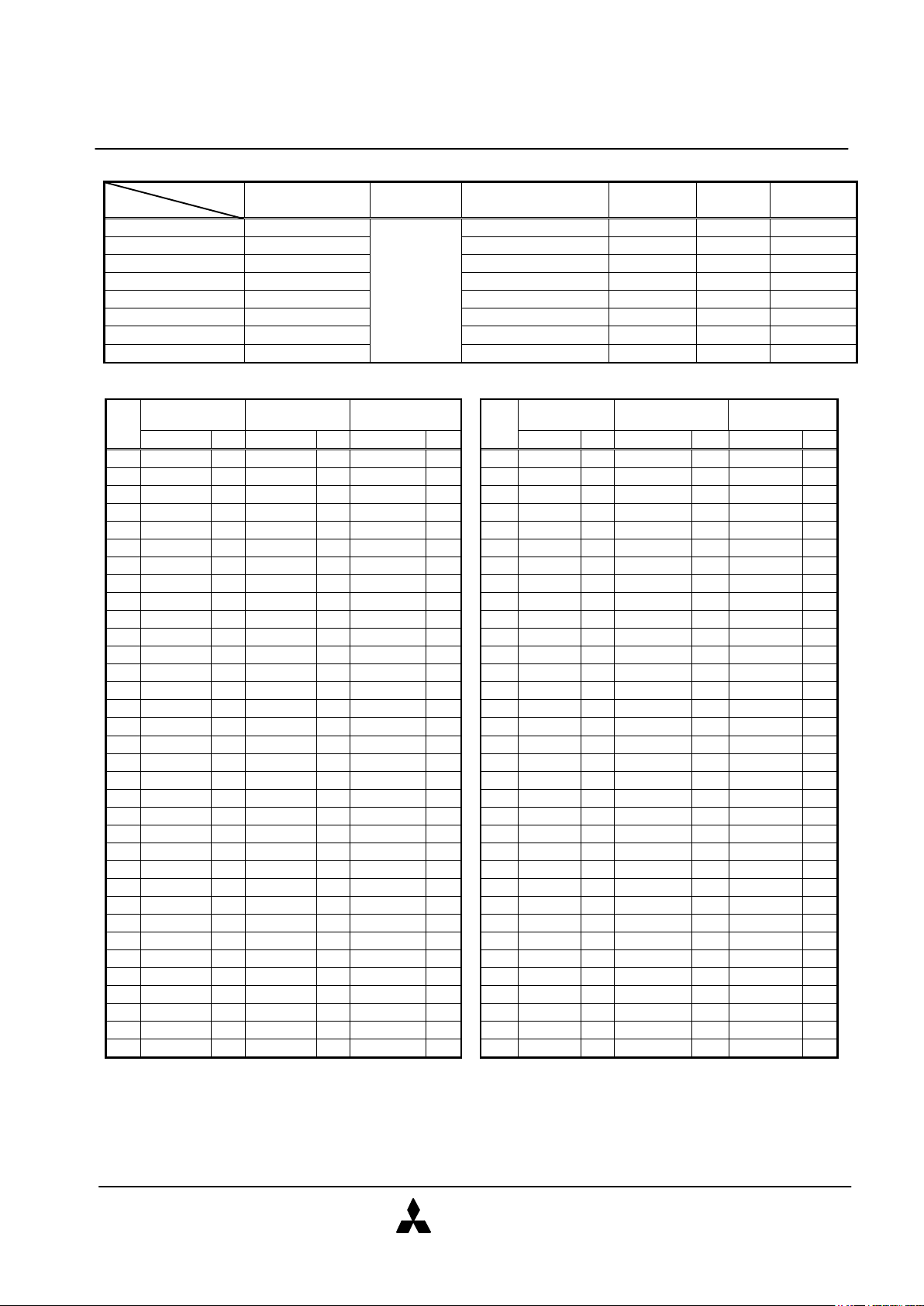
PRODUCT LIST
Memory
capacity(Bytes)
Data Bus
width(bits)
Memory Cylinder Head Sector
MF007M5-03ATxx 7,864,320 64Mbit Flash x 1 240 2 32
MF0015M-03ATxx 15,728,640 64Mbit Flash x 2 480 2 32
MF0030M-03ATxx 31,457,280 64Mbit Flash x 4 480 4 32
MF0045M-03ATxx 47,185,920 8/16 64Mbit Flash x 6 720 4 32
MF0060M-03ATxx 62,914,560 64Mbit Flash x 8 960 4 32
MF0075M-03ATxx 78,643,200 64Mbit Flash x 10 600 8 32
MF0090M-03ATxx 94,371,840 64Mbit Flash x 12 720 8 32
MF0105M-03ATxx 110,100,480 64Mbit Flash x 14 840 8 32
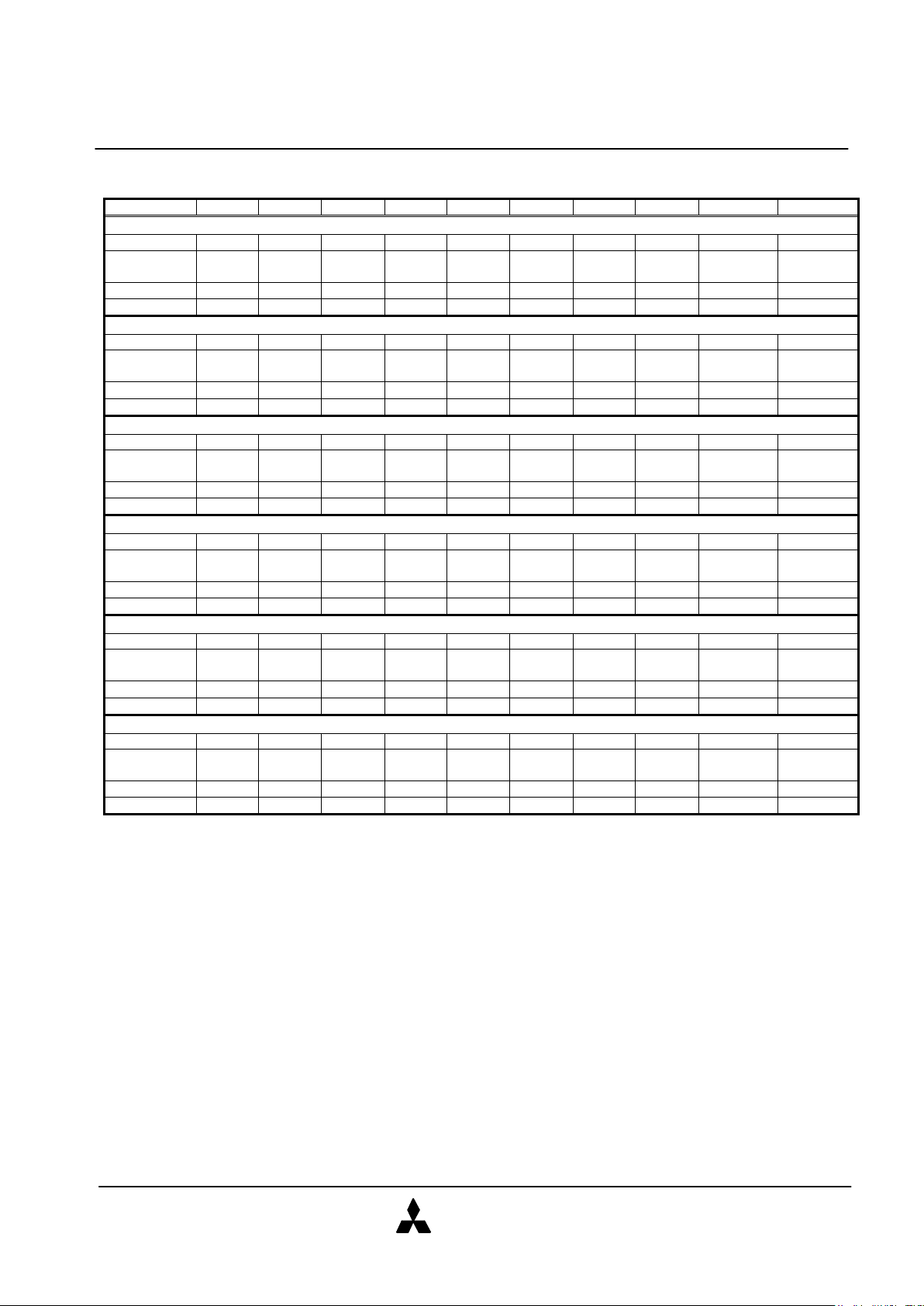
PIN ASSIGNMENT
Pin
PC Card
Memory Mode
PC Card I/O
Mode
IDE ATA
Interface Pin
PC Card
Memory Mode
PC Card I/O
Mode
IDE ATA
Interface
Signal I/O Signal I/O Signal I/O Signal I/O Signal I/O Signal I/O
1 GND - GND - GND - 35 GND - GND - GND 2 D3 I/O D3 I/O D3 I/O 36 CD1# O CD1# O CD1# O
3 D4 I/O D4 I/O D4 I/O 37 D11 I/O D11 I/O D11 I/O
4 D5 I/O D5 I/O D5 I/O 38 D12 I/O D12 I/O D12 I/O
5 D6 I/O D6 I/O D6 I/O 39 D13 I/O D13 I/O D13 I/O
6 D7 I/O D7 I/O D7 I/O 40 D14 I/O D14 I/O D14 I/O
7 CE1# I CE1# I CS0# I 41 D15 I/O D15 I/O D15 I/O
8 A10 I A10 I N.U - 42 CE2# I CE2# I CS1# I
9 OE# I OE# I ATA SEL# I 43 VS1# O VS1# O VS1# O
10 N.C - N.C - N.C - 44 N.U - IORD# I IORD# I
11 A9 I A9 I N.U - 45 N.U - IOWR# I IOWR# I
12 A8 I A8 I N.U - 46 N.C - N.C - N.C 13 N.C - N.C - N.C - 47 N.C - N.C - N.C 14 N.C - N.C - N.C - 48 N.C - N.C - N.C 15 WE# I WE# I WE# I 49 N.C - N.C - N.C 16 READY O IREQ# O INTRQ O 50 N.C - N.C - N.C 17 Vcc - Vcc - Vcc - 51 Vcc - Vcc - Vcc 18 N.C - N.C - N.C - 52 N.C - N.C - N.C 19 N.C - N.C - N.C - 53 N.C - N.C - N.C 20 N.C - N.C - N.C - 54 N.C - N.C - N.C 21 N.C - N.C - N.C - 55 N.C - N.C - N.C 22 A7 I A7 I N.U - 56 CSEL I CSEL I CSEL I
23 A6 I A6 I N.U - 57 VS2# O VS2# O VS2# O
24 A5 I A5 I N.U - 58 RESET I RESET I RESET# I
25 A4 I A4 I N.U - 59 WAIT# O WAIT# O IORDY O
26 A3 I A3 I N.U - 60 N.U - INPACK# O INPACK# O
27 A2 I A2 I A2 I 61 REG# I REG# I REG# I
28 A1 I A1 I A1 I 62 BVD2 O SPKR# O DASP# I/O
29 A0 I A0 I A0 I 63 BVD1 O STSCHG# O PDIAG# I/O
30 D0 I/O D0 I/O D0 I/O 64 D8 I/O D8 I/O D8 I/O
31 D1 I/O D1 I/O D1 I/O 65 D9 I/O D9 I/O D9 I/O
32 D2 I/O D2 I/O D2 I/O 66 D10 I/O D10 I/O D10 I/O
33 WP O IOIS16# O IOCS16# O 67 CD2# O CD2# O CD2# O
34 GND - GND - GND - 68 GND - GND - GND -
N.C = Not connected internally. N.U = Not used.
MITSUBISHI STORAGE CARD
ATA PC CARDS
MITSUBISHI
ELECTRIC
3 1997.Nov. Rev. 1.2
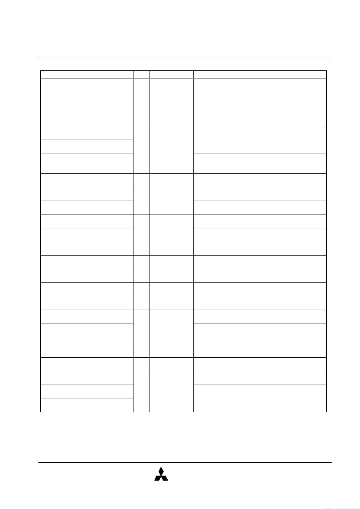
Signal Description
Signal Name I/O Pin No. Description
Address bus[A10-A0] I 8, 11, 12, 22,
23, 24, 25, 26,
27, 28, 29
Signals A10-A0 are address bus. A0 is invalid in
word mode. A10 is the MSB and A0 is the LSB.
Data bus[D15-D0] I/O 41, 40, 39, 38,
37, 66, 65, 64,
6, 5, 4, 3,
Signals D15-D0 are data bus. D0 is the LSB of the
Even Byte of the Word. D8 is the LSB of the Odd
Byte of the Word.
2 ,32,31, 30
Card Enable[CE1#, CE2#]
(PC Card Memory Mode)
I 7, 42 CE1# and CE2# are low active card select signals.
Card Enable[CE1#, CE2#]
(PC Card I/O Mode)
Chip Select[CS0#, CS1#]
(IDE ATA Interface)
In IDE ATA Interface, CS0 is used to select the
Command Block Registers. CS1 is used to select
the Control Block Registers.
Output Enable[OE#]
(PC Card Memory Mode)
I 9 OE# is used to gate Attribute and Common Memory
Read data from the ATA Card.
Output Enable[OE#]
(PC Card I/O Mode)
OE# is used to gate Attribute Memory Read data
from the ATA Card.
ATA SEL#
(IDE ATA Interface)
To enable IDE ATA Interface, this input should be
grounded by the host.
Write Enable[WE#]
(PC Card Memory Mode)
I 15 WE# is used for strobing Attribute and Common
Memory Write data into the ATA Card.
Write Enable[WE#]
(PC Card I/O Mode)
WE# is used for strobing Attribute Memory Write
data into the ATA Card.
Write Enable[WE#]
(IDE ATA Interface)
This input should be connected Vcc by the host.
I/O Read[IORD#]
(PC Card I/O Mode)
I 44 IORD# is used to read data from the Card’s I/O
space.
I/O Read[IORD#]
(IDE ATA Interface)
I/O Write[IOWR#]
(PC Card I/O Mode)
I 45 IOWR# is used to write data to the Card’s I/O
space.
I/O Write[IOWR#]
(IDE ATA Interface)
Ready[READY]
(PC Card Memory Mode)
O 16 READY signal is set high when the ATA Card is
ready to accept a new data transfer operation.
IREQ#
(PC Card I/O Mode)
This signal of low level is indicates that the card is
requesting software service to host, and high level
indicates that the card is not requesting.
INTRQ
(IDE ATA Interface)
This signal is active high interrupt request to the
host.
Card Detection[CD1#, CD2#] O 36, 67 CD1# and CD2# provided for proper detection of
PC Card insertion.
Write Protect[WP]
(PC Card Memory Mode)
O 33 This signal is held low because this card does not
have a write protect switch.
IOIS16#
(PC Card I/O Mode)
This output signal is asserted when the I/O port
address is capable of 16-bit access.
IOCS16#
(IDE ATA Interface)
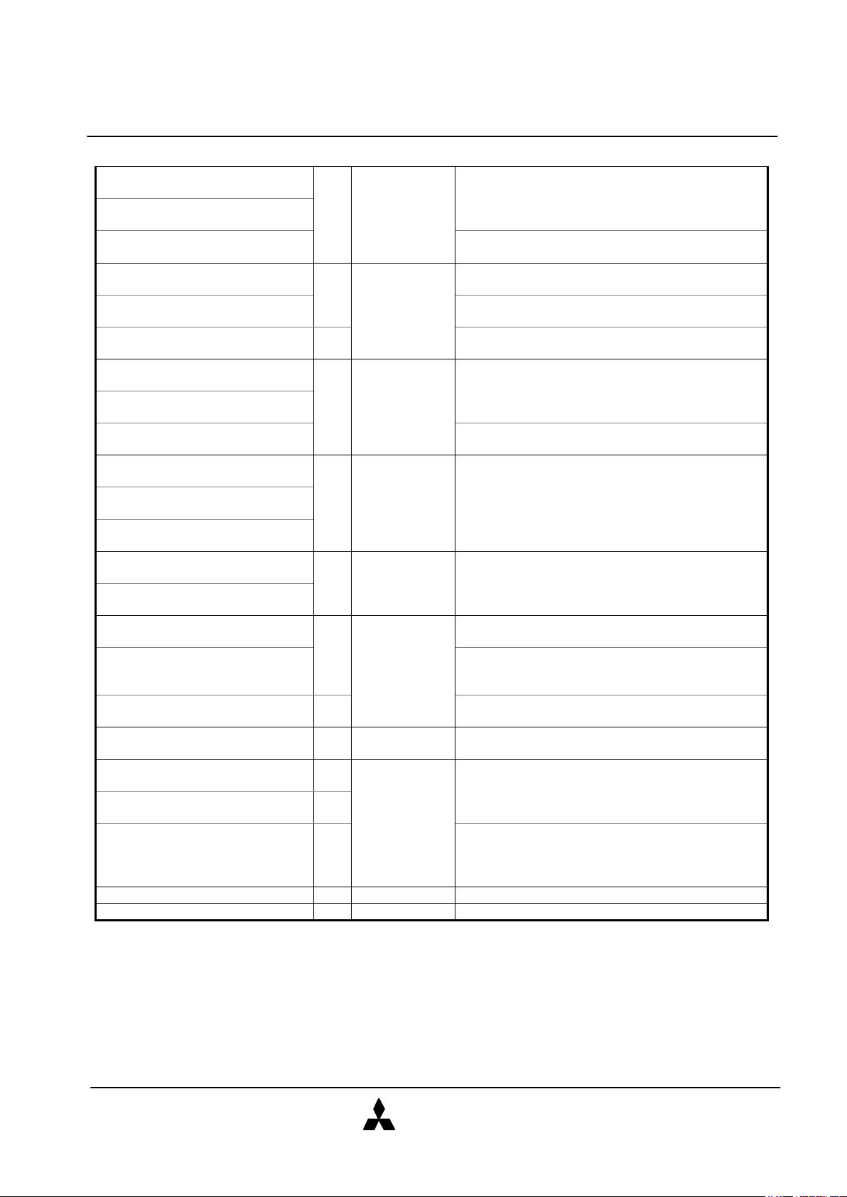
MITSUBISHI STORAGE CARD
ATA PC CARDS
MITSUBISHI
ELECTRIC
4 1997.Nov. Rev. 1.2
Attribute Memory Select[REG#]
(PC Card Memory Mode)
I 61 When this signal is asserted, access is limited to
Attribute Memory with OE#/WE# and I/O Space with
Attribute Memory Select[REG#]
(PC Card I/O Mode)
IORD#/IOWR#.
Attribute Memory Select[REG#]
(IDE ATA Interface)
This input signal is not used for this mode and
should be connected to Vcc by the host.
Battery Voltage Detect[BVD2]
(PC Card Memory Mode)
O 62 This output is driven to a high-level.
Audio Digital Waveform[SPKR#]
(PC Card I/O Mode)
SPKR# is kept negated because this Card does not
have digital audio output.
DASP#
(IDE ATA Interface)
I/O This signal is the DISK Active/Slave Present signal
in the Master/Slave handshake protocol.
Card Reset[RESET]
(PC Card Memory Mode)
I 58 By assertion of this signal, all registers of this Card
are cleared. This signal should be kept to High-Z by
Card Reset[RESET]
(PC Card I/O Mode)
the host for at least 1ms after Vcc applied.
Card Reset[RESET#]
(IDE ATA Interface)
This input pin is the active low hardware reset from
the host.
Wait[WAIT#]
(PC card Memory Mode)
O 59 This signal is asserted to delay completion of the
memory or I/O access cycle.
Wait[WAIT#]
(PC card I/O Mode)
IORDY
(IDE ATA Interface)
Input Port Acknowledge[INPACK#]
(PC Card I/O Mode)
O 60 This signal is asserted when the Card is selected
and can respond to an I/O Read cycle at the
Input Port Acknowledge[INPACK#]
(IDE ATA Interface)
address on the address bus.
Battery Voltage Detect[BVD1]
(PC Card Memory Mode)
O 63 This output is driven to a high-level.
STSCHG#
(PC Card I/O Mode)
This signal is asserted low to alert the host to
changes in the status of Configuration Status
Register in the Attribute Memory Space.
PDIAG#
(IDE ATA Interface)
I/O This signal is the Pass Diagnostic signal in the
Master/Slave handshake protocol.
Voltage Sense[VS1, VS2] O 43, 57 VS1 is grounded so that the Card CIS can be read
at 3.3V and VS2 is N.C.
Cable Select[CSEL]
(PC card Memory Mode)
- 56 This signal is not used for this mode.
Cable Select[CSEL]
(PC card I/O Mode)
-
Cable Select[CSEL]
(IDE ATA Interface)
I This signal is used to configure this Card as a
Master or a Slave. When this signal is grounded,
this Card is configured as a Master. When this
signal is Open, this Card is configure as a Slave.
Vcc - 17, 51 5V or 3.3V power.
GND - 1, 34, 35, 68 Ground.
MITSUBISHI STORAGE CARD
ATA PC CARDS
MITSUBISHI
ELECTRIC
5 1997.Nov. Rev. 1.2
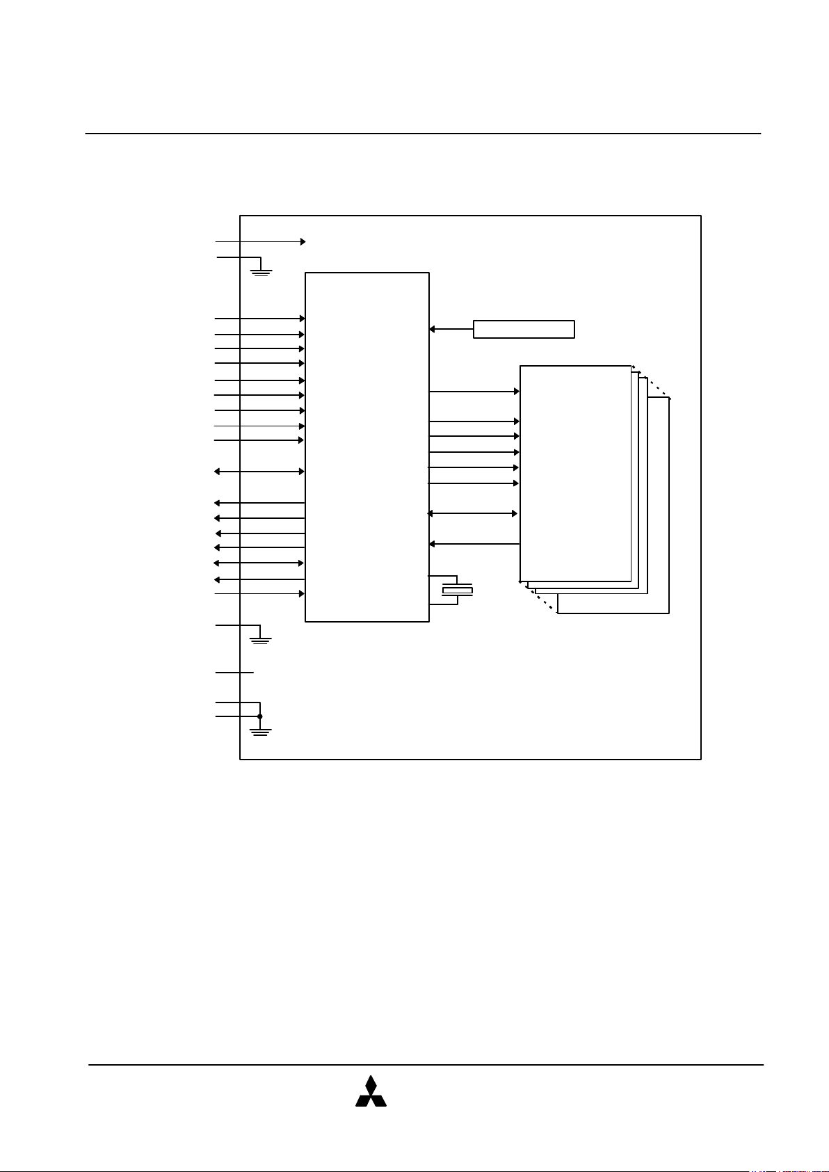
BLOCK DIAGRAM
Vcc
GND
A10-A0
CE1#/CS0#
CE2#/CS1#
OE#/ATA SEL#
WE#
IORD#
IOWR#
REG#
RESET/RESET#
D15-D0
READY/IREQ#/INTRQ
WP/IOIS16#/IOCS16#
INPACK#
BVD1/STSCHG#/PDIAG#
BVD2/SPKR#/DASP#
WAIT#/IORDY
CSEL
VS1
VS2
CD1#
CD2#
Controller
POR#
RES#
CE#
OE#
WE#
CDE#
SC
I/O7-I/O0
R/B#
XIN
XOUT
64Mbit AND
Flash Memory
(x14)
64Mbit AND
Flash Memory
(x14)
RESET Circuit
Open
X-TAL
Internal Vcc
MITSUBISHI STORAGE CARD
ATA PC CARDS
MITSUBISHI
ELECTRIC
6 1997.Nov. Rev. 1.2
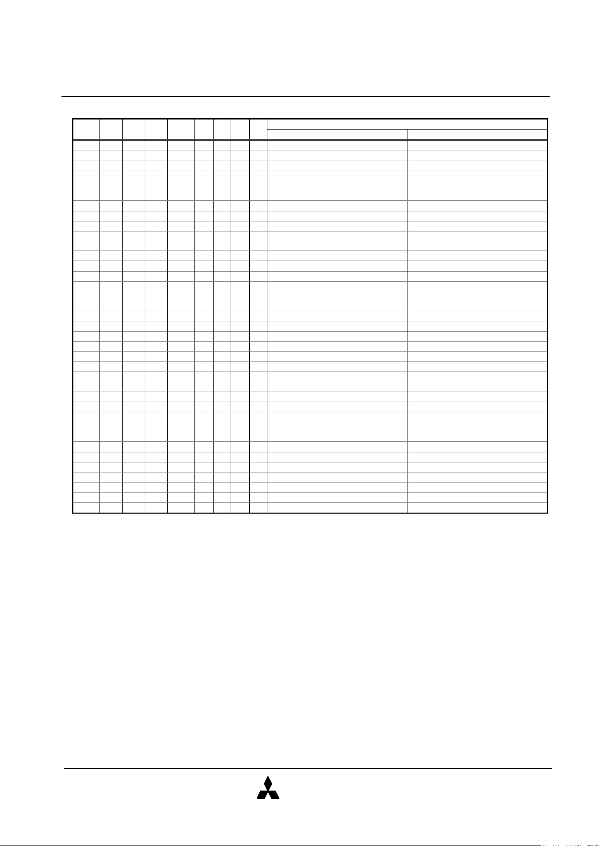
FUNCTION TABLE
Function REG# CE2# CE1# A0 OE# WE# IORD# IOWR# D15-D8 D7-D0
Attribute Memory Read Function
Standby X H H X X X X X High-Z High-Z
Byte Access
L H L L L H H H High-Z Even Byte
L H L H L H H H High-Z Invalid
Word Access
L L L X L H H H Invalid Even Byte
Odd Byte
L L H X L H H H Invalid High-Z
Attribute Memory Write Function
Standby X H H X X X X X don’t care don’t care
Byte Access
L H L L H L H H don’t care Even Byte
L H L H H L H H don’t care don’t care
Word Access
L L L X H L H H don’t care Even Byte
Odd Byte
L L H X H L H H don’t care don’t care
Common Memory Read Function
Standby X H H X X X X X High-Z High-Z
Byte Access
H H L L L H H H High-Z Even Byte
H H L H L H H H High-Z Odd Byte
Word Access
H L L X L H H H Odd Byte Even Byte
Odd Byte
H L H X L H H H Odd Byte High-Z
Common Memory Write Function
Standby X H H X X X X X don’t care don’t care
Byte Access
H H L L H L H H don’t care Even Byte
H H L H H L H H don’t care Odd Byte
Word Access
H L L X H L H H Odd Byte Even Byte
Odd Byte
H L H X H L H H Odd Byte don’t care
I/O Read Function
Standby X H H X X X X X High-Z High-Z
Byte Access
L H L L H H L H High-Z Even Byte
L H L H H H L H High-Z Odd Byte
Word Access
L L L X H H L H Odd Byte Even Byte
Odd Byte
L L H X H H L H Odd Byte High-Z
I/O Write Function
Standby X H H X X X X X don’t care don’t care
Byte Access
L H L L H H H L don’t care Even Byte
L H L H H H H L don’t care Odd Byte
Word Access
L L L X H H H L Odd Byte Even Byte
Odd Byte
L L H X H H H L Odd Byte don’t care
MITSUBISHI STORAGE CARD
ATA PC CARDS
MITSUBISHI
ELECTRIC
7 1997.Nov. Rev. 1.2
Memory mapped mode(Index=0)
REG# CE2# CE1# A10 A9-A4 A3 A2 A1 A0 Register
OE#=”L” WE#=“L”
1 0 0 0 x 0 0 0 x Data Register(D15-D0) Data Register(D15-D0)
1 1 0 0 x 0 0 0 0 Data Register[Even, Odd](D7-D0) Data Register[Even, Odd](D7-D0)
1 1 0 0 x 0 0 0 1 Error Register(D7-D0) Feature Register(D7-D0)
1 0 1 0 x 0 0 0 x Error Register(D15-D8) Feature Register(D15-D8)
1 0 0 0 x 0 0 1 x Sector Count Register(D7-D0)
Sector Number Register(D15-D8)
Sector Count Register(D7-D0)
Sector Number Register(D15-D8)
1 1 0 0 x 0 0 1 0 Sector Count Register(D7-D0) Sector Count Register(D7-D0)
1 1 0 0 x 0 0 1 1 Sector Number Register(D7-D0) Sector Number Register(D7-D0)
1 0 1 0 x 0 0 1 x Sector Number Register(D15-D8) Sector Number Register(D15-D8)
1 0 0 0 x 0 1 0 x Cylinder Low Register(D7-D0)
Cylinder High Register(D15-D8)
Cylinder Low Register(D7-D0)
Cylinder High Register(D15-D8)
1 1 0 0 x 0 1 0 0 Cylinder Low Register(D7-D0) Cylinder Low Register(D7-D0)
1 1 0 0 x 0 1 0 1 Cylinder High Register(D7-D0) Cylinder High Register(D7-D0)
1 0 1 0 x 0 1 0 x Cylinder High Register(D15-D8) Cylinder High Register(D15-D8)
1 0 0 0 x 0 1 1 x Drive Head Register(D7-D0)
Status Register(D15-D8)
Drive Head Register(D7-D0)
Command Register(D15-D8)
1 1 0 0 x 0 1 1 0 Drive Head Register(D7-D0) Drive Head Register(D7-D0)
1 1 0 0 x 0 1 1 1 Status Register(D7-D0) Command Register(D7-D0)
1 0 1 0 x 0 1 1 x Status Register(D15-D8) Command Register(D15-D8)
1 0 0 0 x 1 0 0 x Data Register(D15-D0) Data Register(D15-D0)
1 1 0 0 x 1 0 0 0 Data Register[Even, Odd](D7-D0) Data Register[Even, Odd](D7-D0)
1 1 0 0 x 1 0 0 1 Data Register[Odd](D7-D0) Data Register[Odd](D7-D0)
1 0 1 0 x 1 0 0 x Data Register[Odd](D15-D8) Data Register[Odd](D15-D8)
1 0 0 0 x 1 1 0 x invalid(D7-D0)
Error Register(D15-D8)
invalid(D7-D0)
Feature Register(D15-D8)
1 1 0 0 x 1 1 0 0 invalid invalid
1 1 0 0 x 1 1 0 1 Error Register(D7-D0) Feature Register(D7-D0)
1 0 1 0 x 1 1 0 x Error Register(D15-D8) Feature Register(D15-D8)
1 0 0 0 x 1 1 1 x Alt. Status Register(D7-D0)
Drive Address Register(D15-D8)
Device Control Register(D7-D0)
invalid
1 1 0 0 x 1 1 1 0 Alt. Status Register(D7-D0) Device Control Register(D7-D0)
1 1 0 0 x 1 1 1 1 Drive Address Register(D7-D0) invalid
1 0 1 0 x 1 1 1 x Drive Address Register(D15-D8) invalid
1 0 0 1 x x x x x Data Register(D15-D0) Data Register(D15-D0)
1 1 0 1 x x x x 0 Data Register[Even, Odd](D7-D0) Data Register[Even, Odd](D7-D0)
1 1 0 1 x x x x 1 Data Register[Odd](D7-D0) Data Register[Odd](D7-D0)
1 0 1 1 x x x x x Data Register[Odd](D15-D8) Data Register[Odd](D15-D8)
MITSUBISHI STORAGE CARD
ATA PC CARDS
MITSUBISHI
ELECTRIC
8 1997.Nov. Rev. 1.2
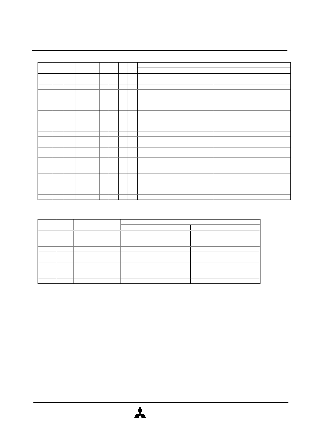
Contiguous I/O Map(Index=1)
REG# CE2# CE1# A9-A4 A3 A2 A1 A0 Register
IORD#=”L” IOWR#=“L”
0 0 0 x 0 0 0 x Data Register(D15-D0) Data Register(D15-D0)
0 1 0 x 0 0 0 0 Data Register[Even, Odd](D7-D0) Data Register[Even, Odd](D7-D0)
0 1 0 x 0 0 0 1 Error Register(D7-D0) Feature Register(D7-D0)
0 0 1 x 0 0 0 x Error Register(D15-D8) Feature Register(D15-D8)
0 0 0 x 0 0 1 0 Sector Count Register(D7-D0)
Sector Number Register(D15-D8)
Sector Count Register(D7-D0)
Sector Number Register(D15-D8)
0 1 0 x 0 0 1 0 Sector Count Register(D7-D0) Sector Count Register(D7-D0)
0 1 0 x 0 0 1 1 Sector Number Register(D7-D0) Sector Number Register(D7-D0)
0 0 1 x 0 0 1 x Sector Number Register(D15-D8) Sector Number Register(D15-D8)
0 0 0 x 0 1 0 0 Cylinder Low Register(D7-D0)
Cylinder High Register(D15-D8)
Cylinder Low Register(D7-D0)
Cylinder High Register(D15-D8)
0 1 0 x 0 1 0 0 Cylinder Low Register(D7-D0) Cylinder Low Register(D7-D0)
0 1 0 x 0 1 0 1 Cylinder High Register(D7-D0) Cylinder High Register(D7-D0)
0 0 1 x 0 1 0 x Cylinder High Register(D15-D8) Cylinder High Register(D15-D8)
0 0 0 x 0 1 1 0 Drive Head Register(D7-D0)
Status Register(D15-D8)
Drive Head Register(D7-D0)
Command Register(D15-D8)
0 1 0 x 0 1 1 0 Drive Head Register(D7-D0) Drive Head Register(D7-D0)
0 1 0 x 0 1 1 1 Status Register(D7-D0) Command Register(D7-D0)
0 0 1 x 0 1 1 x Status Register(D15-D8) Command Register(D15-D8)
0 0 0 x 1 0 0 x Data Register(D15-D0) Data Register(D15-D0)
0 1 0 x 1 0 0 0 Data Register[Even, Odd](D7-D0) Data Register[Even, Odd](D7-D0)
0 1 0 x 1 0 0 1 Data Register[Odd](D7-D0) Data Register[Odd](D7-D0)
0 0 1 x 1 0 0 x Data Register[Odd](D15-D8) Data Register[Odd](D15-D8)
0 0 0 x 1 1 0 0 invalid(D7-D0)
Error Register(D15-D8)
invalid(D7-D0)
Feature Register(D15-D8)
0 1 0 x 1 1 0 0 invalid invalid
0 1 0 x 1 1 0 1 Error Register(D7-D0) Feature Register(D7-D0)
0 0 1 x 1 1 0 x Error Register(D15-D8) Feature Register(D15-D8)
0 0 0 x 1 1 1 0 Alt. Status Register(D7-D0)
Drive Address Register(D15-D8)
Device Control Register(D7-D0)
invalid
0 1 0 x 1 1 1 0 Alt. Status Register(D7-D0) Device Control Register(D7-D0)
0 1 0 x 1 1 1 1 Drive Address Register(D7-D0) invalid
0 0 1 x 1 1 1 x Drive Address Register(D15-D8) invalid
MITSUBISHI STORAGE CARD
ATA PC CARDS
MITSUBISHI
ELECTRIC
9 1997.Nov. Rev. 1.2
Primary(Secondary) I/O(Index=2, 3)
REG# CE2# CE1# A9-A4 A3 A2 A1 A0 Register
IORD#=”L” IOWR#=“L”
0 0 0 1Fh(17h) 0 0 0 x Data Register(D15-D0) Data Register(D15-D0)
0 1 0 1Fh(17h) 0 0 0 0 Data Register[Even, Odd](D7-D0) Data Register[Even, Odd](D7-D0)
0 1 0 1Fh(17h) 0 0 0 1 Error Register(D7-D0) Feature Register(D7-D0)
0 0 1 1Fh(17h) 0 0 0 x Error Register(D15-D8) Feature Register(D15-D8)
0 0 0 1Fh(17h) 0 0 1 0 Sector Count Register(D7-D0)
Sector Number Register(D15-D8)
Sector Count Register(D7-D0)
Sector Number Register(D15-D8)
0 1 0 1Fh(17h) 0 0 1 0 Sector Count Register(D7-D0) Sector Count Register(D7-D0)
0 1 0 1Fh(17h) 0 0 1 1 Sector Number Register(D7-D0) Sector Number Register(D7-D0)
0 0 1 1Fh(17h) 0 0 1 x Sector Number Register(D15-D8) Sector Number Register(D15-D8)
0 0 0 1Fh(17h) 0 1 0 0 Cylinder Low Register(D7-D0)
Cylinder High Register(D15-D8)
Cylinder Low Register(D7-D0)
Cylinder High Register(D15-D8)
0 1 0 1Fh(17h) 0 1 0 0 Cylinder Low Register(D7-D0) Cylinder Low Register(D7-D0)
0 1 0 1Fh(17h) 0 1 0 1 Cylinder High Register(D7-D0) Cylinder High Register(D7-D0)
0 0 1 1Fh(17h) 0 1 0 x Cylinder High Register(D15-D8) Cylinder High Register(D15-D8)
0 0 0 1Fh(17h) 0 1 1 0 Drive Head Register(D7-D0)
Status Register(D15-D8)
Drive Head Register(D7-D0)
Command Register(D15-D8)
0 1 0 1Fh(17h) 0 1 1 0 Drive Head Register(D7-D0) Drive Head Register(D7-D0)
0 1 0 1Fh(17h) 0 1 1 1 Status Register(D7-D0) Command Register(D7-D0)
0 0 1 1Fh(17h) 0 1 1 x Status Register(D15-D8) Command Register(D15-D8)
0 0 0 3Fh(37h) 1 1 1 0 Alt. Status Register(D7-D0)
Drive Address Register(D15-D8)
Device Control Register(D7-D0)
invalid
0 1 0 3Fh(37h) 1 1 1 0 Alt. Status Register(D7-D0) Device Control Register(D7-D0)
0 1 0 3Fh(37h) 1 1 1 1 Drive Address Register(D7-D0) invalid
0 0 1 3Fh(37h) 1 1 1 x Drive Address Register(D15-D8) invalid
IDE ATA Interface
CS1# CS0# A2-A0 Register
IORD#=”L” IOWR#=“L”
1 0 0h Data Register(D15-D0) Data Register(D15-D0)
1 0 1h Error Register(D7-D0) Feature Register(D7-D0)
1 0 2h Sector Count Register(D7-D0) Sector Count Register(D7-D0)
1 0 3h Sector Number Register(D7-D0) Sector Number Register(D7-D0)
1 0 4h Cylinder Low Register(D7-D0) Cylinder Low Register(D7-D0)
1 0 5h Cylinder High Register(D7-D0) Cylinder High Register(D7-D0)
1 0 6h Drive Head Register(D7-D0) Drive Head Register(D7-D0)
1 0 7h Status Register(D7-D0) Command Register(D7-D0)
0 1 6h Alt. Status Register(D7-D0) Device Control Register(D7-D0)
0 1 7h Drive Address Register(D7-D0) invalid
 Loading...