

Mitsubishi MF0060M-03AT, MF0045M-03AT, MF007M5-03AT, MF0090M-03AT, MF0075M-03AT Datasheet
...
MITSUBISHI STORAGE CARD
ATA PC CARDS
MITSUBISHI
ELECTRIC
1 1997.Nov. Rev. 1.2
8/16-bit Data Bus
Flash ATA PC Card
Connector Type
Two- piece 68-pin
DESCRIPTION
Mitsubishi’s Flash ATA cards provide large
memory capacities on a device approximately
the size of a credit card
(85.6mm×54mm×3.3mm). The cards use a 8/16
bit data bus.
Available in 7.5MB, 15MB, 30MB, 45MB,
60MB, 75MB, 90MB and 105MB capacities,
Mitsubishi’s Flash ATA cards conform to the
JEIDA/PCMCIA standard.
In default mode, the ATA card operates in PC
Card compliant sockets. It conforms to
PCMCIA2.1, JEIDA4.2 and PC Card Standard.
When the OE# signal is asserted low level by
the Host system in power on cycle, the
Mitsubishi’s Flash ATA cards can be selected
in a IDE ATA interface. It uses the ATA
command set so no software drivers are
required.
MF007M5-03ATxx
MF0015M-03ATxx
MF0030M-03ATxx
MF0045M-03ATxx
MF0060M-03ATxx
MF0075M-03ATxx
MF0090M-03ATxx
MF0105M-03ATxx
FEATURES
68 pin PC Card Standard Type-I PC Card
Single 5V or 3.3V Supply
Card density of up to 105MB maximum
Four PC Card ATA and IDE ATA modes
Nonvolatile, No Batteries Required
High reliability based on internal ECC
function
Auto power-down mode
APPLICATIONS
Computers Office automation
Digital Camera Industrial
Data Communication Consumer
MITSUBISHI STORAGE CARD
ATA PC CARDS
MITSUBISHI
ELECTRIC
2 1997.Nov. Rev. 1.2
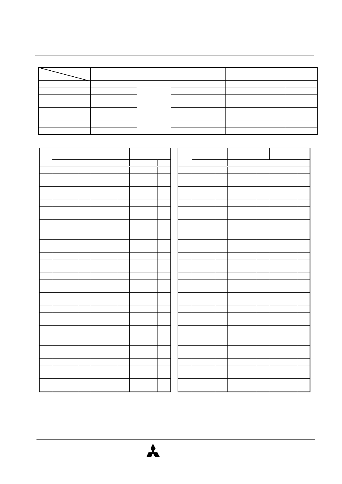
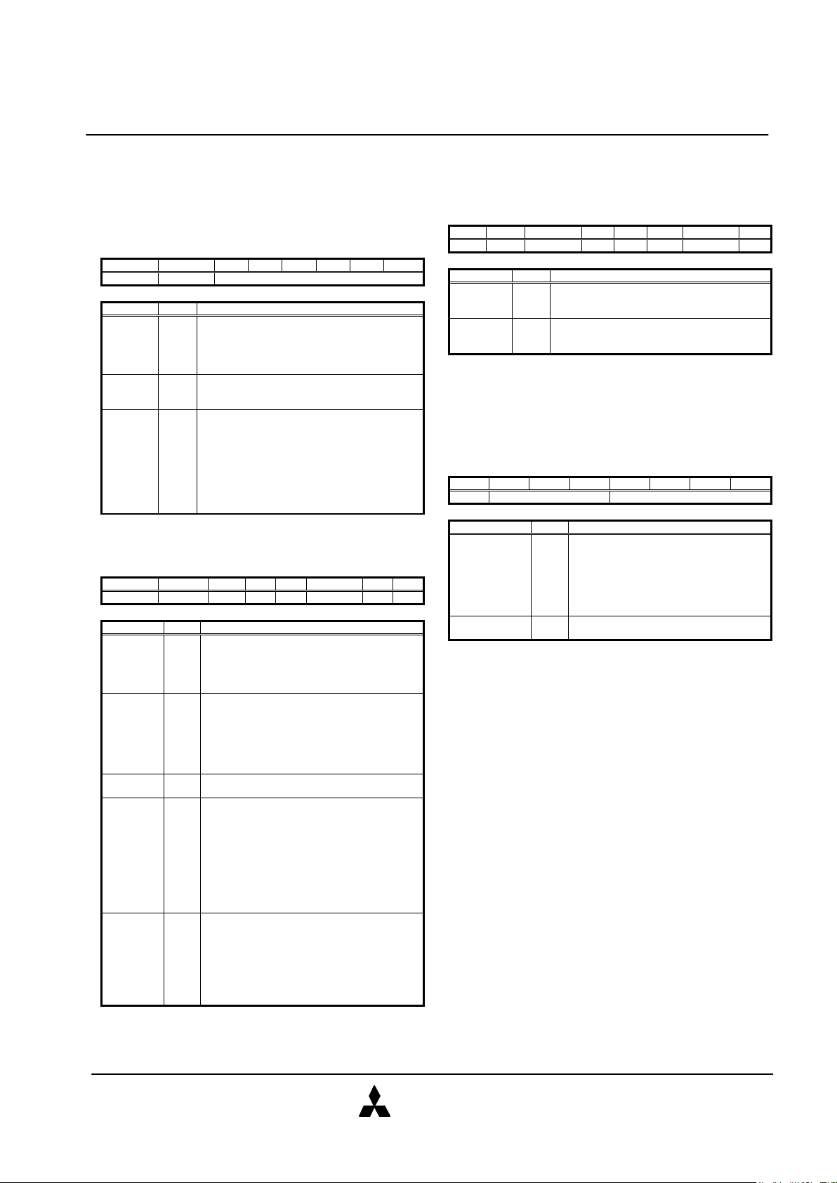
PRODUCT LIST
Memory
capacity(Bytes)
Data Bus
width(bits)
Memory Cylinder Head Sector
MF007M5-03ATxx 7,864,320 64Mbit Flash x 1 240 2 32
MF0015M-03ATxx 15,728,640 64Mbit Flash x 2 480 2 32
MF0030M-03ATxx 31,457,280 64Mbit Flash x 4 480 4 32
MF0045M-03ATxx 47,185,920 8/16 64Mbit Flash x 6 720 4 32
MF0060M-03ATxx 62,914,560 64Mbit Flash x 8 960 4 32
MF0075M-03ATxx 78,643,200 64Mbit Flash x 10 600 8 32
MF0090M-03ATxx 94,371,840 64Mbit Flash x 12 720 8 32
MF0105M-03ATxx 110,100,480 64Mbit Flash x 14 840 8 32
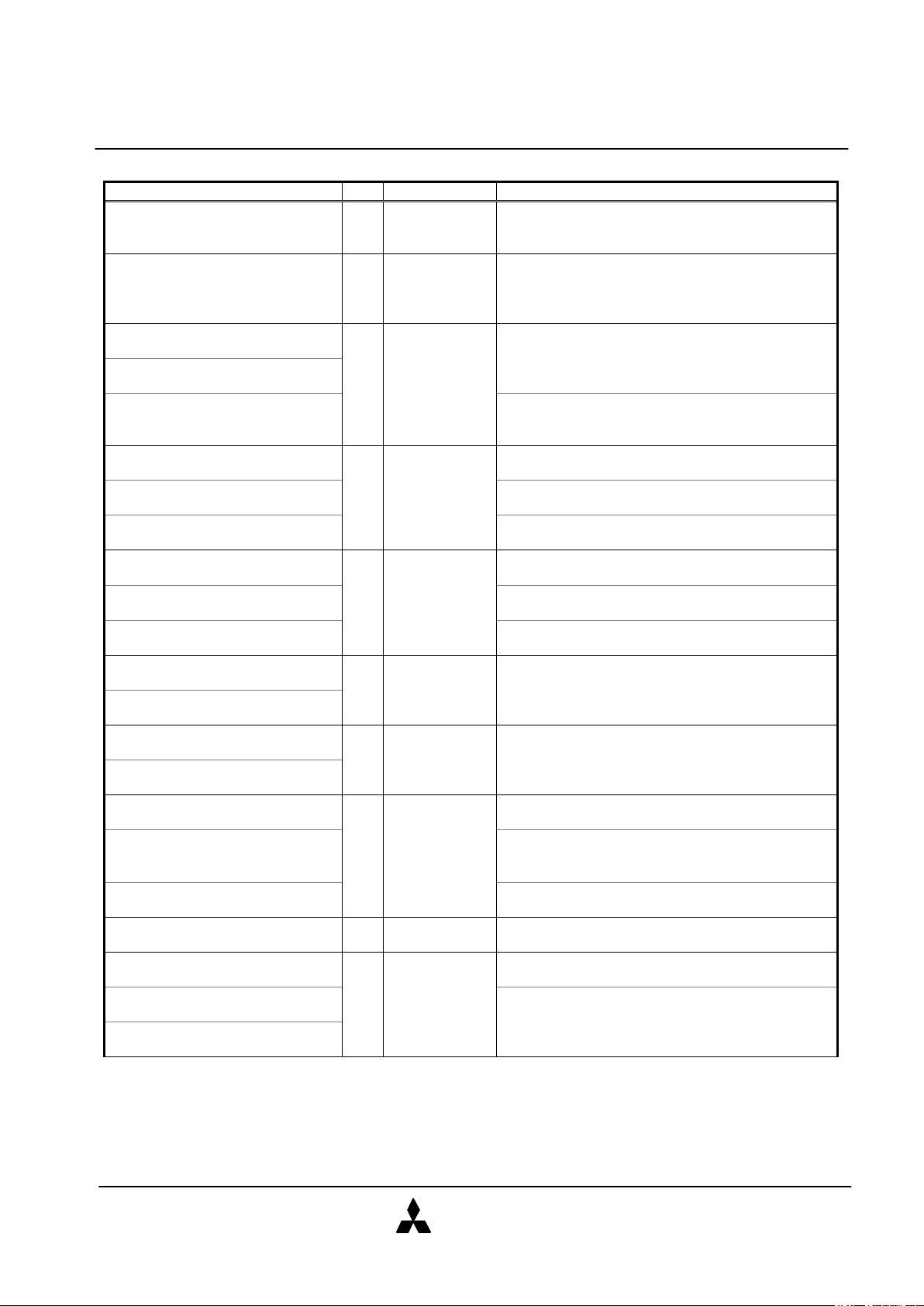
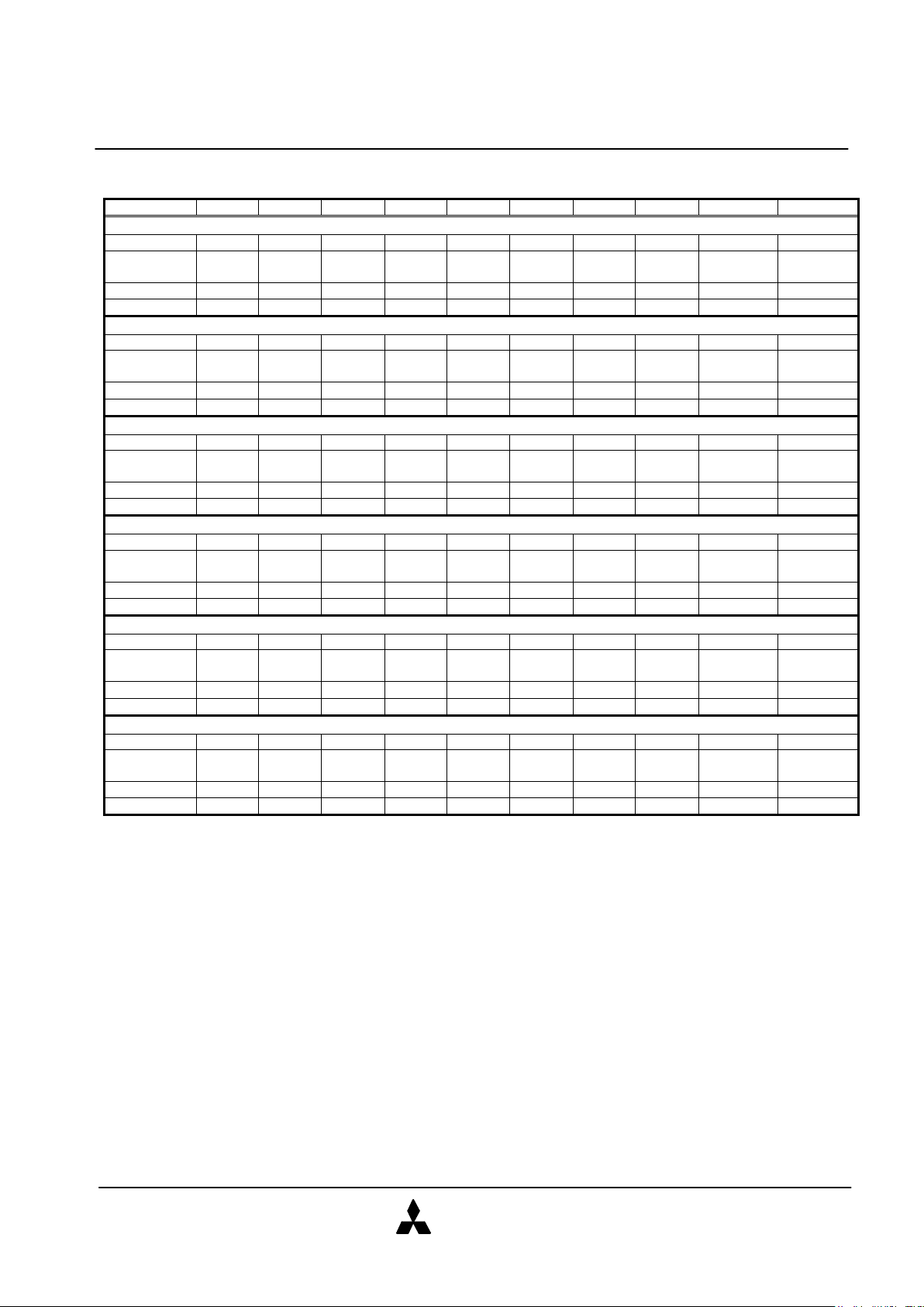
PIN ASSIGNMENT
Pin
PC Card
Memory Mode
PC Card I/O
Mode
IDE ATA
Interface Pin
PC Card
Memory Mode
PC Card I/O
Mode
IDE ATA
Interface
Signal I/O Signal I/O Signal I/O Signal I/O Signal I/O Signal I/O
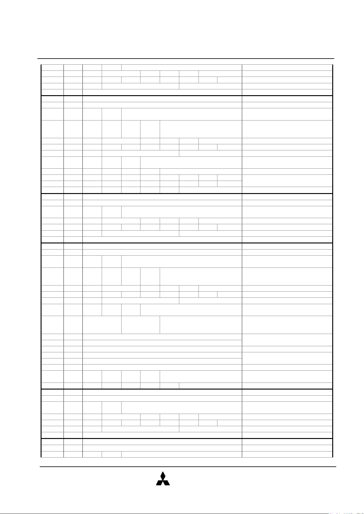
1 GND - GND - GND - 35 GND - GND - GND 2 D3 I/O D3 I/O D3 I/O 36 CD1# O CD1# O CD1# O
3 D4 I/O D4 I/O D4 I/O 37 D11 I/O D11 I/O D11 I/O
4 D5 I/O D5 I/O D5 I/O 38 D12 I/O D12 I/O D12 I/O
5 D6 I/O D6 I/O D6 I/O 39 D13 I/O D13 I/O D13 I/O
6 D7 I/O D7 I/O D7 I/O 40 D14 I/O D14 I/O D14 I/O
7 CE1# I CE1# I CS0# I 41 D15 I/O D15 I/O D15 I/O
8 A10 I A10 I N.U - 42 CE2# I CE2# I CS1# I
9 OE# I OE# I ATA SEL# I 43 VS1# O VS1# O VS1# O
10 N.C - N.C - N.C - 44 N.U - IORD# I IORD# I
11 A9 I A9 I N.U - 45 N.U - IOWR# I IOWR# I
12 A8 I A8 I N.U - 46 N.C - N.C - N.C 13 N.C - N.C - N.C - 47 N.C - N.C - N.C 14 N.C - N.C - N.C - 48 N.C - N.C - N.C 15 WE# I WE# I WE# I 49 N.C - N.C - N.C 16 READY O IREQ# O INTRQ O 50 N.C - N.C - N.C 17 Vcc - Vcc - Vcc - 51 Vcc - Vcc - Vcc 18 N.C - N.C - N.C - 52 N.C - N.C - N.C 19 N.C - N.C - N.C - 53 N.C - N.C - N.C 20 N.C - N.C - N.C - 54 N.C - N.C - N.C 21 N.C - N.C - N.C - 55 N.C - N.C - N.C 22 A7 I A7 I N.U - 56 CSEL I CSEL I CSEL I
23 A6 I A6 I N.U - 57 VS2# O VS2# O VS2# O
24 A5 I A5 I N.U - 58 RESET I RESET I RESET# I
25 A4 I A4 I N.U - 59 WAIT# O WAIT# O IORDY O
26 A3 I A3 I N.U - 60 N.U - INPACK# O INPACK# O
27 A2 I A2 I A2 I 61 REG# I REG# I REG# I
28 A1 I A1 I A1 I 62 BVD2 O SPKR# O DASP# I/O
29 A0 I A0 I A0 I 63 BVD1 O STSCHG# O PDIAG# I/O
30 D0 I/O D0 I/O D0 I/O 64 D8 I/O D8 I/O D8 I/O
31 D1 I/O D1 I/O D1 I/O 65 D9 I/O D9 I/O D9 I/O
32 D2 I/O D2 I/O D2 I/O 66 D10 I/O D10 I/O D10 I/O
33 WP O IOIS16# O IOCS16# O 67 CD2# O CD2# O CD2# O
34 GND - GND - GND - 68 GND - GND - GND -
N.C = Not connected internally. N.U = Not used.
MITSUBISHI STORAGE CARD
ATA PC CARDS
MITSUBISHI
ELECTRIC
3 1997.Nov. Rev. 1.2
Signal Description
Signal Name I/O Pin No. Description
Address bus[A10-A0] I 8, 11, 12, 22,
23, 24, 25, 26,
27, 28, 29
Signals A10-A0 are address bus. A0 is invalid in
word mode. A10 is the MSB and A0 is the LSB.
Data bus[D15-D0] I/O 41, 40, 39, 38,
37, 66, 65, 64,
6, 5, 4, 3,
Signals D15-D0 are data bus. D0 is the LSB of the
Even Byte of the Word. D8 is the LSB of the Odd
Byte of the Word.
2 ,32,31, 30
Card Enable[CE1#, CE2#]
(PC Card Memory Mode)
I 7, 42 CE1# and CE2# are low active card select signals.
Card Enable[CE1#, CE2#]
(PC Card I/O Mode)
Chip Select[CS0#, CS1#]
(IDE ATA Interface)
In IDE ATA Interface, CS0 is used to select the
Command Block Registers. CS1 is used to select
the Control Block Registers.
Output Enable[OE#]
(PC Card Memory Mode)
I 9 OE# is used to gate Attribute and Common Memory
Read data from the ATA Card.
Output Enable[OE#]
(PC Card I/O Mode)
OE# is used to gate Attribute Memory Read data
from the ATA Card.
ATA SEL#
(IDE ATA Interface)
To enable IDE ATA Interface, this input should be
grounded by the host.
Write Enable[WE#]
(PC Card Memory Mode)
I 15 WE# is used for strobing Attribute and Common
Memory Write data into the ATA Card.
Write Enable[WE#]
(PC Card I/O Mode)
WE# is used for strobing Attribute Memory Write
data into the ATA Card.
Write Enable[WE#]
(IDE ATA Interface)
This input should be connected Vcc by the host.
I/O Read[IORD#]
(PC Card I/O Mode)
I 44 IORD# is used to read data from the Card’s I/O
space.
I/O Read[IORD#]
(IDE ATA Interface)
I/O Write[IOWR#]
(PC Card I/O Mode)
I 45 IOWR# is used to write data to the Card’s I/O
space.
I/O Write[IOWR#]
(IDE ATA Interface)
Ready[READY]
(PC Card Memory Mode)
O 16 READY signal is set high when the ATA Card is
ready to accept a new data transfer operation.
IREQ#
(PC Card I/O Mode)
This signal of low level is indicates that the card is
requesting software service to host, and high level
indicates that the card is not requesting.
INTRQ
(IDE ATA Interface)
This signal is active high interrupt request to the
host.
Card Detection[CD1#, CD2#] O 36, 67 CD1# and CD2# provided for proper detection of
PC Card insertion.
Write Protect[WP]
(PC Card Memory Mode)
O 33 This signal is held low because this card does not
have a write protect switch.
IOIS16#
(PC Card I/O Mode)
This output signal is asserted when the I/O port
address is capable of 16-bit access.
IOCS16#
(IDE ATA Interface)
MITSUBISHI STORAGE CARD
ATA PC CARDS
MITSUBISHI
ELECTRIC
4 1997.Nov. Rev. 1.2
Attribute Memory Select[REG#]
(PC Card Memory Mode)
I 61 When this signal is asserted, access is limited to
Attribute Memory with OE#/WE# and I/O Space with
Attribute Memory Select[REG#]
(PC Card I/O Mode)
IORD#/IOWR#.
Attribute Memory Select[REG#]
(IDE ATA Interface)
This input signal is not used for this mode and
should be connected to Vcc by the host.
Battery Voltage Detect[BVD2]
(PC Card Memory Mode)
O 62 This output is driven to a high-level.
Audio Digital Waveform[SPKR#]
(PC Card I/O Mode)
SPKR# is kept negated because this Card does not
have digital audio output.
DASP#
(IDE ATA Interface)
I/O This signal is the DISK Active/Slave Present signal
in the Master/Slave handshake protocol.
Card Reset[RESET]
(PC Card Memory Mode)
I 58 By assertion of this signal, all registers of this Card
are cleared. This signal should be kept to High-Z by
Card Reset[RESET]
(PC Card I/O Mode)
the host for at least 1ms after Vcc applied.
Card Reset[RESET#]
(IDE ATA Interface)
This input pin is the active low hardware reset from
the host.
Wait[WAIT#]
(PC card Memory Mode)
O 59 This signal is asserted to delay completion of the
memory or I/O access cycle.
Wait[WAIT#]
(PC card I/O Mode)
IORDY
(IDE ATA Interface)
Input Port Acknowledge[INPACK#]
(PC Card I/O Mode)
O 60 This signal is asserted when the Card is selected
and can respond to an I/O Read cycle at the
Input Port Acknowledge[INPACK#]
(IDE ATA Interface)
address on the address bus.
Battery Voltage Detect[BVD1]
(PC Card Memory Mode)
O 63 This output is driven to a high-level.
STSCHG#
(PC Card I/O Mode)
This signal is asserted low to alert the host to
changes in the status of Configuration Status
Register in the Attribute Memory Space.
PDIAG#
(IDE ATA Interface)
I/O This signal is the Pass Diagnostic signal in the
Master/Slave handshake protocol.
Voltage Sense[VS1, VS2] O 43, 57 VS1 is grounded so that the Card CIS can be read
at 3.3V and VS2 is N.C.
Cable Select[CSEL]
(PC card Memory Mode)
- 56 This signal is not used for this mode.
Cable Select[CSEL]
(PC card I/O Mode)
-
Cable Select[CSEL]
(IDE ATA Interface)
I This signal is used to configure this Card as a
Master or a Slave. When this signal is grounded,
this Card is configured as a Master. When this
signal is Open, this Card is configure as a Slave.
Vcc - 17, 51 5V or 3.3V power.
GND - 1, 34, 35, 68 Ground.
MITSUBISHI STORAGE CARD
ATA PC CARDS
MITSUBISHI
ELECTRIC
5 1997.Nov. Rev. 1.2
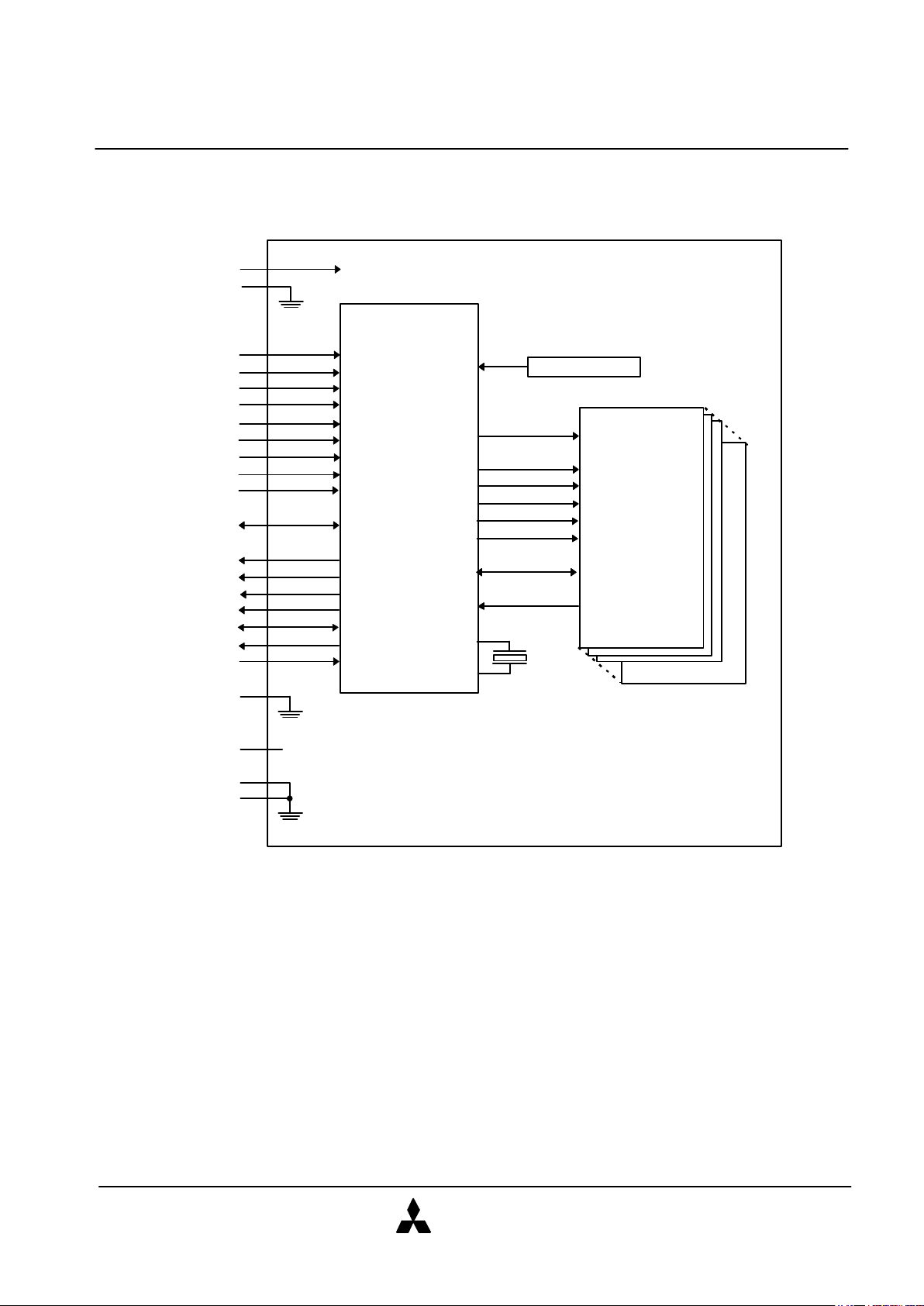
BLOCK DIAGRAM
Vcc
GND
A10-A0
CE1#/CS0#
CE2#/CS1#
OE#/ATA SEL#
WE#
IORD#
IOWR#
REG#
RESET/RESET#
D15-D0
READY/IREQ#/INTRQ
WP/IOIS16#/IOCS16#
INPACK#
BVD1/STSCHG#/PDIAG#
BVD2/SPKR#/DASP#
WAIT#/IORDY
CSEL
VS1
VS2
CD1#
CD2#
Controller
POR#
RES#
CE#
OE#
WE#
CDE#
SC
I/O7-I/O0
R/B#
XIN
XOUT
64Mbit AND
Flash Memory
(x14)
64Mbit AND
Flash Memory
(x14)
RESET Circuit
Open
X-TAL
Internal Vcc
MITSUBISHI STORAGE CARD
ATA PC CARDS
MITSUBISHI
ELECTRIC
6 1997.Nov. Rev. 1.2
FUNCTION TABLE
Function REG# CE2# CE1# A0 OE# WE# IORD# IOWR# D15-D8 D7-D0
Attribute Memory Read Function
Standby X H H X X X X X High-Z High-Z
Byte Access
L H L L L H H H High-Z Even Byte
L H L H L H H H High-Z Invalid
Word Access
L L L X L H H H Invalid Even Byte
Odd Byte
L L H X L H H H Invalid High-Z
Attribute Memory Write Function
Standby X H H X X X X X don’t care don’t care
Byte Access
L H L L H L H H don’t care Even Byte
L H L H H L H H don’t care don’t care
Word Access
L L L X H L H H don’t care Even Byte
Odd Byte
L L H X H L H H don’t care don’t care
Common Memory Read Function
Standby X H H X X X X X High-Z High-Z
Byte Access
H H L L L H H H High-Z Even Byte
H H L H L H H H High-Z Odd Byte
Word Access
H L L X L H H H Odd Byte Even Byte
Odd Byte
H L H X L H H H Odd Byte High-Z
Common Memory Write Function
Standby X H H X X X X X don’t care don’t care
Byte Access
H H L L H L H H don’t care Even Byte
H H L H H L H H don’t care Odd Byte
Word Access
H L L X H L H H Odd Byte Even Byte
Odd Byte
H L H X H L H H Odd Byte don’t care
I/O Read Function
Standby X H H X X X X X High-Z High-Z
Byte Access
L H L L H H L H High-Z Even Byte
L H L H H H L H High-Z Odd Byte
Word Access
L L L X H H L H Odd Byte Even Byte
Odd Byte
L L H X H H L H Odd Byte High-Z
I/O Write Function
Standby X H H X X X X X don’t care don’t care
Byte Access
L H L L H H H L don’t care Even Byte
L H L H H H H L don’t care Odd Byte
Word Access
L L L X H H H L Odd Byte Even Byte
Odd Byte
L L H X H H H L Odd Byte don’t care
MITSUBISHI STORAGE CARD
ATA PC CARDS
MITSUBISHI
ELECTRIC
7 1997.Nov. Rev. 1.2
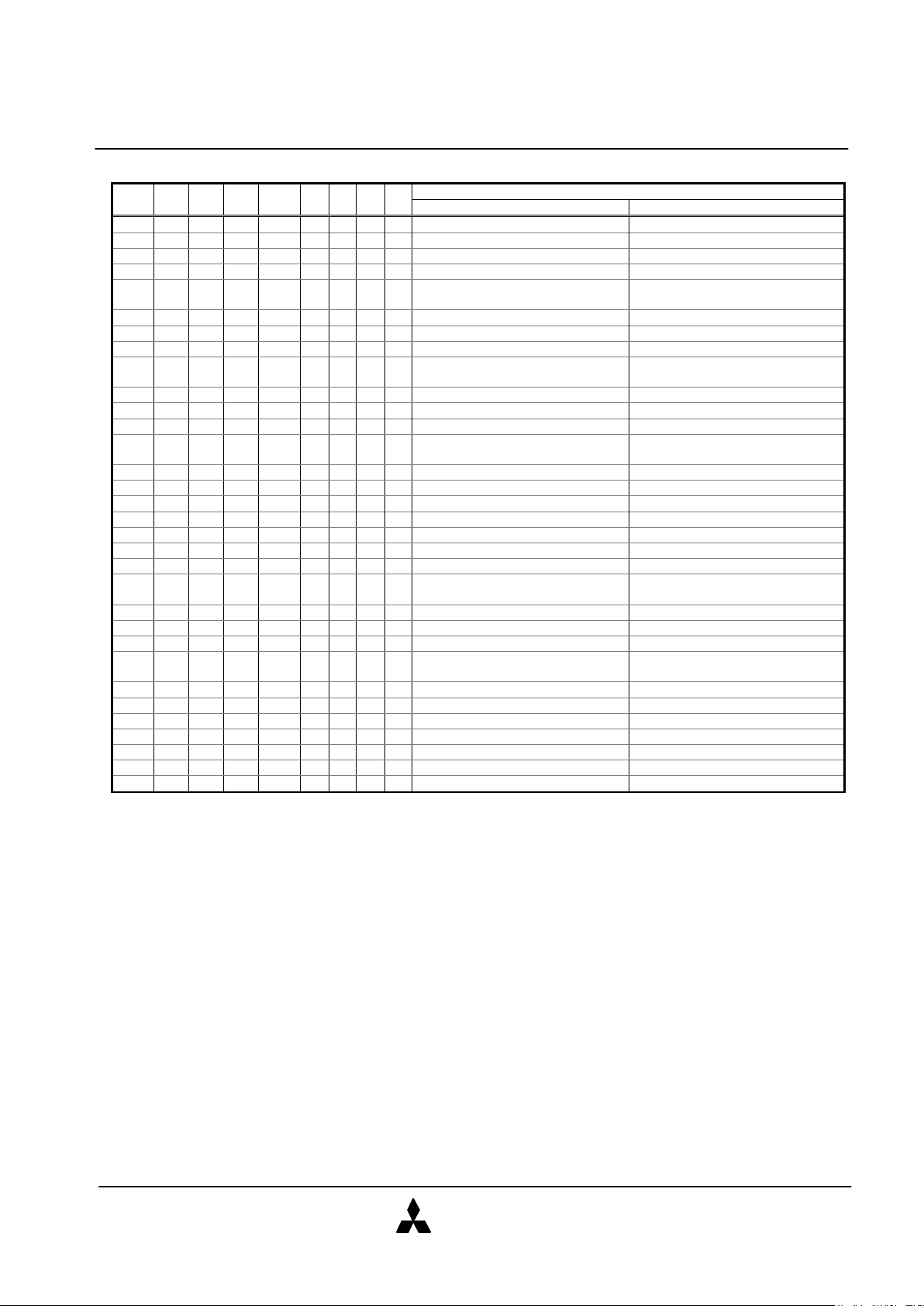
Memory mapped mode(Index=0)
REG# CE2# CE1# A10 A9-A4 A3 A2 A1 A0 Register
OE#=”L” WE#=“L”
1 0 0 0 x 0 0 0 x Data Register(D15-D0) Data Register(D15-D0)
1 1 0 0 x 0 0 0 0 Data Register[Even, Odd](D7-D0) Data Register[Even, Odd](D7-D0)
1 1 0 0 x 0 0 0 1 Error Register(D7-D0) Feature Register(D7-D0)
1 0 1 0 x 0 0 0 x Error Register(D15-D8) Feature Register(D15-D8)
1 0 0 0 x 0 0 1 x Sector Count Register(D7-D0)
Sector Number Register(D15-D8)
Sector Count Register(D7-D0)
Sector Number Register(D15-D8)
1 1 0 0 x 0 0 1 0 Sector Count Register(D7-D0) Sector Count Register(D7-D0)
1 1 0 0 x 0 0 1 1 Sector Number Register(D7-D0) Sector Number Register(D7-D0)
1 0 1 0 x 0 0 1 x Sector Number Register(D15-D8) Sector Number Register(D15-D8)
1 0 0 0 x 0 1 0 x Cylinder Low Register(D7-D0)
Cylinder High Register(D15-D8)
Cylinder Low Register(D7-D0)
Cylinder High Register(D15-D8)
1 1 0 0 x 0 1 0 0 Cylinder Low Register(D7-D0) Cylinder Low Register(D7-D0)
1 1 0 0 x 0 1 0 1 Cylinder High Register(D7-D0) Cylinder High Register(D7-D0)
1 0 1 0 x 0 1 0 x Cylinder High Register(D15-D8) Cylinder High Register(D15-D8)
1 0 0 0 x 0 1 1 x Drive Head Register(D7-D0)
Status Register(D15-D8)
Drive Head Register(D7-D0)
Command Register(D15-D8)
1 1 0 0 x 0 1 1 0 Drive Head Register(D7-D0) Drive Head Register(D7-D0)
1 1 0 0 x 0 1 1 1 Status Register(D7-D0) Command Register(D7-D0)
1 0 1 0 x 0 1 1 x Status Register(D15-D8) Command Register(D15-D8)
1 0 0 0 x 1 0 0 x Data Register(D15-D0) Data Register(D15-D0)
1 1 0 0 x 1 0 0 0 Data Register[Even, Odd](D7-D0) Data Register[Even, Odd](D7-D0)
1 1 0 0 x 1 0 0 1 Data Register[Odd](D7-D0) Data Register[Odd](D7-D0)
1 0 1 0 x 1 0 0 x Data Register[Odd](D15-D8) Data Register[Odd](D15-D8)
1 0 0 0 x 1 1 0 x invalid(D7-D0)
Error Register(D15-D8)
invalid(D7-D0)
Feature Register(D15-D8)
1 1 0 0 x 1 1 0 0 invalid invalid
1 1 0 0 x 1 1 0 1 Error Register(D7-D0) Feature Register(D7-D0)
1 0 1 0 x 1 1 0 x Error Register(D15-D8) Feature Register(D15-D8)
1 0 0 0 x 1 1 1 x Alt. Status Register(D7-D0)
Drive Address Register(D15-D8)
Device Control Register(D7-D0)
invalid
1 1 0 0 x 1 1 1 0 Alt. Status Register(D7-D0) Device Control Register(D7-D0)
1 1 0 0 x 1 1 1 1 Drive Address Register(D7-D0) invalid
1 0 1 0 x 1 1 1 x Drive Address Register(D15-D8) invalid
1 0 0 1 x x x x x Data Register(D15-D0) Data Register(D15-D0)
1 1 0 1 x x x x 0 Data Register[Even, Odd](D7-D0) Data Register[Even, Odd](D7-D0)
1 1 0 1 x x x x 1 Data Register[Odd](D7-D0) Data Register[Odd](D7-D0)
1 0 1 1 x x x x x Data Register[Odd](D15-D8) Data Register[Odd](D15-D8)
MITSUBISHI STORAGE CARD
ATA PC CARDS
MITSUBISHI
ELECTRIC
8 1997.Nov. Rev. 1.2
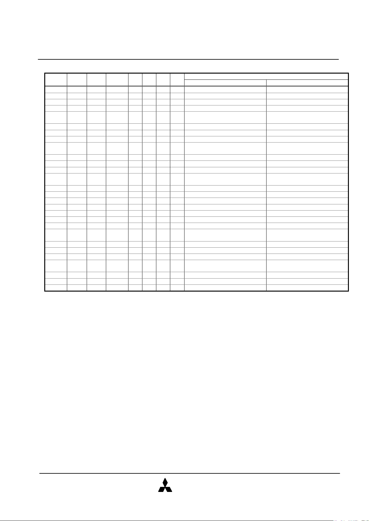
Contiguous I/O Map(Index=1)
REG# CE2# CE1# A9-A4 A3 A2 A1 A0 Register
IORD#=”L” IOWR#=“L”
0 0 0 x 0 0 0 x Data Register(D15-D0) Data Register(D15-D0)
0 1 0 x 0 0 0 0 Data Register[Even, Odd](D7-D0) Data Register[Even, Odd](D7-D0)
0 1 0 x 0 0 0 1 Error Register(D7-D0) Feature Register(D7-D0)
0 0 1 x 0 0 0 x Error Register(D15-D8) Feature Register(D15-D8)
0 0 0 x 0 0 1 0 Sector Count Register(D7-D0)
Sector Number Register(D15-D8)
Sector Count Register(D7-D0)
Sector Number Register(D15-D8)
0 1 0 x 0 0 1 0 Sector Count Register(D7-D0) Sector Count Register(D7-D0)
0 1 0 x 0 0 1 1 Sector Number Register(D7-D0) Sector Number Register(D7-D0)
0 0 1 x 0 0 1 x Sector Number Register(D15-D8) Sector Number Register(D15-D8)
0 0 0 x 0 1 0 0 Cylinder Low Register(D7-D0)
Cylinder High Register(D15-D8)
Cylinder Low Register(D7-D0)
Cylinder High Register(D15-D8)
0 1 0 x 0 1 0 0 Cylinder Low Register(D7-D0) Cylinder Low Register(D7-D0)
0 1 0 x 0 1 0 1 Cylinder High Register(D7-D0) Cylinder High Register(D7-D0)
0 0 1 x 0 1 0 x Cylinder High Register(D15-D8) Cylinder High Register(D15-D8)
0 0 0 x 0 1 1 0 Drive Head Register(D7-D0)
Status Register(D15-D8)
Drive Head Register(D7-D0)
Command Register(D15-D8)
0 1 0 x 0 1 1 0 Drive Head Register(D7-D0) Drive Head Register(D7-D0)
0 1 0 x 0 1 1 1 Status Register(D7-D0) Command Register(D7-D0)
0 0 1 x 0 1 1 x Status Register(D15-D8) Command Register(D15-D8)
0 0 0 x 1 0 0 x Data Register(D15-D0) Data Register(D15-D0)
0 1 0 x 1 0 0 0 Data Register[Even, Odd](D7-D0) Data Register[Even, Odd](D7-D0)
0 1 0 x 1 0 0 1 Data Register[Odd](D7-D0) Data Register[Odd](D7-D0)
0 0 1 x 1 0 0 x Data Register[Odd](D15-D8) Data Register[Odd](D15-D8)
0 0 0 x 1 1 0 0 invalid(D7-D0)
Error Register(D15-D8)
invalid(D7-D0)
Feature Register(D15-D8)
0 1 0 x 1 1 0 0 invalid invalid
0 1 0 x 1 1 0 1 Error Register(D7-D0) Feature Register(D7-D0)
0 0 1 x 1 1 0 x Error Register(D15-D8) Feature Register(D15-D8)
0 0 0 x 1 1 1 0 Alt. Status Register(D7-D0)
Drive Address Register(D15-D8)
Device Control Register(D7-D0)
invalid
0 1 0 x 1 1 1 0 Alt. Status Register(D7-D0) Device Control Register(D7-D0)
0 1 0 x 1 1 1 1 Drive Address Register(D7-D0) invalid
0 0 1 x 1 1 1 x Drive Address Register(D15-D8) invalid
MITSUBISHI STORAGE CARD
ATA PC CARDS
MITSUBISHI
ELECTRIC
9 1997.Nov. Rev. 1.2
Primary(Secondary) I/O(Index=2, 3)
REG# CE2# CE1# A9-A4 A3 A2 A1 A0 Register
IORD#=”L” IOWR#=“L”
0 0 0 1Fh(17h) 0 0 0 x Data Register(D15-D0) Data Register(D15-D0)
0 1 0 1Fh(17h) 0 0 0 0 Data Register[Even, Odd](D7-D0) Data Register[Even, Odd](D7-D0)
0 1 0 1Fh(17h) 0 0 0 1 Error Register(D7-D0) Feature Register(D7-D0)
0 0 1 1Fh(17h) 0 0 0 x Error Register(D15-D8) Feature Register(D15-D8)
0 0 0 1Fh(17h) 0 0 1 0 Sector Count Register(D7-D0)
Sector Number Register(D15-D8)
Sector Count Register(D7-D0)
Sector Number Register(D15-D8)
0 1 0 1Fh(17h) 0 0 1 0 Sector Count Register(D7-D0) Sector Count Register(D7-D0)
0 1 0 1Fh(17h) 0 0 1 1 Sector Number Register(D7-D0) Sector Number Register(D7-D0)
0 0 1 1Fh(17h) 0 0 1 x Sector Number Register(D15-D8) Sector Number Register(D15-D8)
0 0 0 1Fh(17h) 0 1 0 0 Cylinder Low Register(D7-D0)
Cylinder High Register(D15-D8)
Cylinder Low Register(D7-D0)
Cylinder High Register(D15-D8)
0 1 0 1Fh(17h) 0 1 0 0 Cylinder Low Register(D7-D0) Cylinder Low Register(D7-D0)
0 1 0 1Fh(17h) 0 1 0 1 Cylinder High Register(D7-D0) Cylinder High Register(D7-D0)
0 0 1 1Fh(17h) 0 1 0 x Cylinder High Register(D15-D8) Cylinder High Register(D15-D8)
0 0 0 1Fh(17h) 0 1 1 0 Drive Head Register(D7-D0)
Status Register(D15-D8)
Drive Head Register(D7-D0)
Command Register(D15-D8)
0 1 0 1Fh(17h) 0 1 1 0 Drive Head Register(D7-D0) Drive Head Register(D7-D0)
0 1 0 1Fh(17h) 0 1 1 1 Status Register(D7-D0) Command Register(D7-D0)
0 0 1 1Fh(17h) 0 1 1 x Status Register(D15-D8) Command Register(D15-D8)
0 0 0 3Fh(37h) 1 1 1 0 Alt. Status Register(D7-D0)
Drive Address Register(D15-D8)
Device Control Register(D7-D0)
invalid
0 1 0 3Fh(37h) 1 1 1 0 Alt. Status Register(D7-D0) Device Control Register(D7-D0)
0 1 0 3Fh(37h) 1 1 1 1 Drive Address Register(D7-D0) invalid
0 0 1 3Fh(37h) 1 1 1 x Drive Address Register(D15-D8) invalid
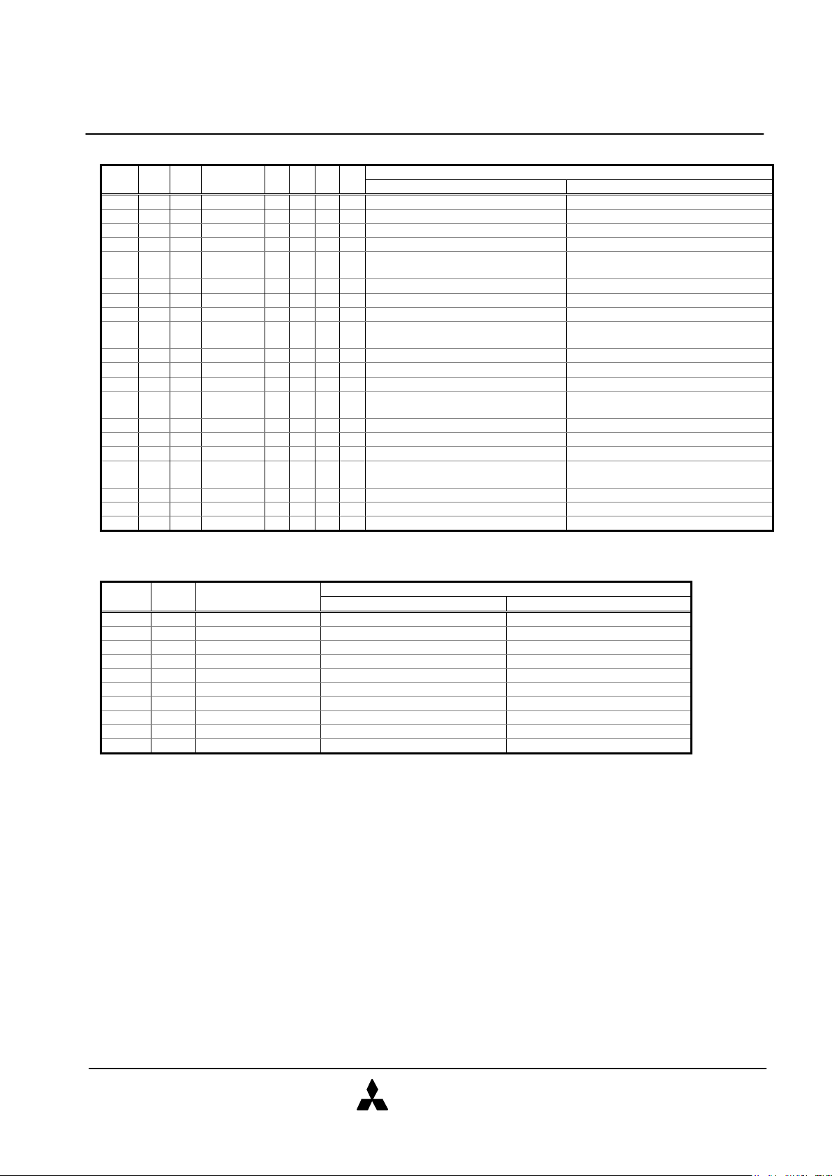
IDE ATA Interface
CS1# CS0# A2-A0 Register
IORD#=”L” IOWR#=“L”
1 0 0h Data Register(D15-D0) Data Register(D15-D0)
1 0 1h Error Register(D7-D0) Feature Register(D7-D0)
1 0 2h Sector Count Register(D7-D0) Sector Count Register(D7-D0)
1 0 3h Sector Number Register(D7-D0) Sector Number Register(D7-D0)
1 0 4h Cylinder Low Register(D7-D0) Cylinder Low Register(D7-D0)
1 0 5h Cylinder High Register(D7-D0) Cylinder High Register(D7-D0)
1 0 6h Drive Head Register(D7-D0) Drive Head Register(D7-D0)
1 0 7h Status Register(D7-D0) Command Register(D7-D0)
0 1 6h Alt. Status Register(D7-D0) Device Control Register(D7-D0)
0 1 7h Drive Address Register(D7-D0) invalid
MITSUBISHI STORAGE CARD
ATA PC CARDS
MITSUBISHI
ELECTRIC
10 1997.Nov. Rev. 1.2
Configuration Register Specifications
Configuration Option Register
This register is used for the configuration of the card
configuration status and for the issuing soft reset to the
card.
D7 D6 D5 D4 D3 D2 D1 D0
SRESET LevIREQ Index
Name R/W Description
SRESET R/W Setting this bit to “1”, places the card in the reset
state. When the host returns this bit to “0”, the
function shall enter the same unconfigured,
reset state as the card does following a powerup and hardware reset.
LevIREQ R/W If this bit is set to “0”, card generates pulse
mode interrupt. If this bit is set to “1”, card
generates level mode interrupts.
Index R/W This bits is used for select operation mode of the
card as follows.
When Power on, Card Hard Reset and Soft
reset, this data is “000000” for the purpose of
Memory card interface recognition.
Index: 0 -> Memory mapped
1 -> Contiguous I/O mapped
2 -> Primary I/O mapped
3 -> Secondary I/O mapped
Configuration and Status Register
This register is used for observing the card state.
D7 D6 D5 D4 D3 D2 D1 D0
Changed SigChg Iois8 0 0 PwrDwn Intr 0
Name R/W Description
Changed R/O This bit indicates that CREADY bit on the Pin
Replacement register is set to “1”. When
Changed bit is set to “1”, STSCHG# pin is held
“L” if the SigChg bit is “1” and the card is
configured for the I/O interface.
SigChg R/W This bit is set or reset by the host for enabling
and disabling the status change
signal(STSCHG# pin). When the card is
configured I/O card interface and this bit is set
to “1”, STSCHG# pin is controlled by Changed
bit. If this bit is set to “0”, STSCHG# pin is kept
“H”.
Iois8 R/W This card is always configured for both 8-bit
and 16-bit I/O, so this bit is ignored.
PwrDwn R/W When this bit is set to “1”, the card enters
Power Down mode. When this bit is reset to
“0”, the host is requesting the card to enter the
active mode. RREADY bit on Pin Replacement
Register becomes BUSY when this bit is
changed. RREADY will not become Ready until
the power state requested has been entered.
This card automatically powers down when it is
idle, and powers back up when it receives a
command.
Intr R/W This bit represents the internal state of the
interrupt request. This bit state is available
whether I/O card interface has been configured
or not. This signal remains true until the
condition which caused the interrupt request
has been serviced. If interrupts are disabled by
the nIEN bit in the Device Control Register, this
bit is a zero.
Pin Replacement Register
This register is used for providing the signal state of
READY signal when the card configured I/O card
interface.
D7 D6 D5 D4 D3 D2 D1 D0
0 0 CREADY 0 1 1 RREADY 0
Name R/W Description
CREADY R/W This bit is set to “1” when the RREADY bit
changes state. This bit may also be written by
the host.
RREADY R/W When read, this bit indicates READY pin
states. When written, this bit acts as a mask
for writing the CREADY bit.
Socket and Copy Register
This register is used for identification of the card from the
other cards. Host can read and write this register. This
register should be set by host before this card’s
Configuration Option register set.
D7 D6 D5 D4 D3 D2 D1 D0
0 Copy Number Socket Number
Name R/W Description
Copy Number R/W This bit indicates the drive number of the
card for twin card configuration.
And the host can select and drive one card
by comparing the number in this field with
the drive number of Drive Head Register.
In the way, the host can perform the card’s
master/slave organization.
Socket
Number
R/W This field indicates to the card that it is
located in the n’th socket.

MITSUBISHI STORAGE CARD
ATA PC CARDS
MITSUBISHI
ELECTRIC
11 1997.Nov. Rev. 1.2
CIS Information
CIS informatoins are defined as follows.
Offset Data 7 6 5 4 3 2 1 0 Description
0000h 01h CISTPL_DEVICE Common Memory device information
0002h 03h TPL_LINK Link to next tuple
Device Type=Dh : Function specific
0004h D9h Device Type WPS Device Speed WPS=1 : No WPS
Device Speed=1 : 250ns
0006h 01h 1x 2K 2kBytes of address space
0008h FFh Marks end of Device Info fields
000Ah 1Ch CISTPL_DEVICE_OC Other Conditions Device information
000Ch 05h TPL_LINK Link to next tuple
000Eh 02h EXT Reserved Vcc MWAIT EXT=0, Vcc=5.0V, Wait is not used.
Device Type=Dh : Function specific
0010h DFh Device Type WPS Device Speed WPS=1 : No WPS
Device Speed=250ns
0012h 01h 1x 2K 2kbytes of address space
0014h FFh Marks end of Other Conditions Device Info
0016h 1Ch CISTPL_DEVICE_OC Other Conditions Device information
0018h 04h TPL_LINK Link to next tuple
001Ah 02h EXT Reserved Vcc MWAIT EXT=0, Vcc=3.3V, Wait is not used.
Device Type=Dh : Function specific
001Ch D9h Device Type WPS Device Speed WPS=1 : No WPS
Device Speed=250ns
001Eh 01h 1x 2K 2kbytes of address space
0020h FFh Marks end of Other Conditions Device Info
0022h 18h CISTPL_JEDEC_C JEDEC Identifier Tuples
0024h 02h TPL_LINK Link to next tuple
0026h DFh JEDEC identifier for first device info entry. PC Card ATA
0028h 01h JEDEC identifiers for remaining device info entries. with no Vpp require for any operation
002Ah 20h CISTPL_MANFID Manufacturer Identification Tuple
002Ch 04h TPL_LINK Link to next tuple
002Eh 1Ch PC Card manufacturer code 001Ch
0030h 00h
0032h 01h manufacturer information 0001h
0034h 00h
0036h 15h CISTPL_VERS_1 Level 1 Version / Product Information
0038h 26h TPL_LINK Link to next tuple
003Ah 04h TPLLV1_MAJOR PCMCIA2.0 / JEIDA4.1
003Ch 01h TPLLV1_MINOR PCMCIA2.0 / JEIDA4.1
003Eh 4Dh TPLLV1_INFO M
0040h 49h I
0042h 54h T
0044h 53h S
0046h 55h U
0048h 42h B
004Ah 49h I
004Ch 53h S
004Eh 48h H
0050h 49h I
0052h 20h
0054h 41h A
0056h 54h T
0058h 41h A
005Ah 20h
005Ch 43h C
005Eh 41h A
0060h 52h R
0062h 44h D
0064h 00h
0066h 4Dh M
0068h 46h F

MITSUBISHI STORAGE CARD
ATA PC CARDS
MITSUBISHI
ELECTRIC
12 1997.Nov. Rev. 1.2
006Ah 30h 0
006Ch 78h x
006Eh 78h x
0070h 78h x
0072h 78h x
0074h 2Dh 0076h 30h 0
0078h 33h 3
007Ah 41h A
007Ch 54h T
007Eh 58h x
0080h 78h x
0082h 00
0084h FFh Marks end of chain.
0086h 21h CISTPL_FUNCID Function Identification Tuple
0088h 02h TPL_LINK Link to next tuple
008Ah 04h Card Function Code PC Card ATA(Fixed Disk)
008Ch 01h Reserved ROM POST ROM=0 : No BIOS ROM
POST=1: Configure card at power on
008Eh 22h CISTPL_FUNCE Function Extension Tuple
0090h 02h TPL_LINK Link to next tuple
0092h 01h Disk Function Extension Tuple Type Disk Interface Type
0094h 01h Disk Interface Type PC Card ATA Interface
0096h 22h CISTPL_FUNCE Function Extension Tuple
0098h 03h TPL_LINK Link to next tuple
009Ah 02h Disk Function Extension Tuple Type Basic PC Card ATA Interface tuple
009Ch 04h RFU D U S V V=0 : No Vpp Required
S=1 : Silicon
U=0 : ID Drive Mfg/SN not Unique
D=0 : Single Drive on Card
009Eh 0Fh RFU I E N P3 P2 P1 P0 P0=1 : Sleep Mode Supported
P1=1 : Standby Mode Supported
P2=1 : Idle Mode Supported
P3=1 : Drive Auto Power Control
N=0 : No Configs exclude I/O port
3F7H/377H
E=0 : Index bit is not emulated
I=0 : IOIS16# use is Unspecified on
Twin Card Configurations
00A0h 1Ah CISTPL_CONF Configuration Tuple
00A2h 05h TPL_LINK Link to next tuple
00A4h 01h RFS RMS RAS RFS=0 : No Reserved Field
RMS=0 : 1 Byte Register Mask
RAS=1 : 2 Byte Config Base Address
00A6h 03h TPCC_LAST Last Index = 3
00A8h 00h TPCC_RADR (lsb) Configuration Registers are located
00AAh 02h TPCC_RADR (msb) at 200H in Reg Space
00ACh 0Fh RFU RFU RFU E S P C I First 4 Configuration Registers present
00AEh 1Bh CISTPL_CFTABLE_ENTRY Configuration Table Entry Tuple
00B0h 08h TPL_LINK Link to next tuple
00B2h C0h I D Configuration Index Interface Byte Follows, Default Entry,
Configuration Index = 0
00B4h 40h W R P B Interface Type Mem Interface; Bvd's and wProt not
used; Ready active and Wait not used
for memory cycles.
00B6h A1h M MS IR IO T P Has Vcc, Mem Space and Misc Info
00B8h 01h R DI PI AI SI HV LV NV Nominal Voltage Only Follows
00BAh 55h X Mantissa Exponent Vcc Nominal is 5 Volts
00BCh 08h Length in 256 bytes pages (lsb) Length of Mem Space is 2 KB
00BEh 00h Length in 256 bytes pages (msb) Starts at 0 on card
00C0h 21h X RFU P RO A T Power Down, Twin Card supported.
00C2h 1Bh CISTPL_CFTABLE_ENTRY Configuration Table Entry Tuple
00C4h 05h TPL_LINK Link to next tuple
00C6h 00h I D Configuration Index No Interface Byte, Non Default Entry,
MITSUBISHI STORAGE CARD
ATA PC CARDS
MITSUBISHI
ELECTRIC
13 1997.Nov. Rev. 1.2
Configuration Index = 0
00C8h 01h M MS IR IO T P Has Vcc Info
00CAh 01h R DI PI AI SI HV LV NV Nominal Voltage Only Follows
00CCh B5h X Mantissa Exponent Vcc Nominal is 3.3 Volts
00CEh 1Eh Extension
00D0h 1Bh CISTPL_CFTABLE_ENTRY Configuration Table Entry Tuple
00D2h 0Ah TPL_LINK Link to next tuple
00D4h C1h I D Configuration Index Interface Byte Follows, Default Entry,
Configuration Index = 1
00D6h 41h W R P B Interface Type I/O Interface; Bvd's and wProt not
used; Ready active and Wait not used
for memory cycles.
00D8h 99h M MS IR IO T P Has Vcc, I/O, IRQ and Misc Info
00DAh 01h R DI PI AI SI HV LV NV Nominal Voltage Only Follows
00DCh 55h X Mantissa Exponent Vcc Nominal is 5 Volts
00DEh 64h R S E IO AddrLines I/O : Range=0, Bus16=1, Bus8=1,
IO AddrLines=4
00E0h F0h S P L M Level or Mask Share=1, Pulse=1, Level=1, Mask=1
00E2h FFh IRQ7 IRQ6 IRQ5 IRQ4 IRQ3 IRQ2 IRQ1 IRQ0 IRQ Level to be routed 0 - 15
00E4h FFh IRQ15 IRQ14 IRQ13 IRQ12 IRQ11 IRQ10 IRQ9 IRQ8 recommended.
00E6h 21h X RFU P RO A T Power Down, Twin Card supported.
00E8h 1Bh CISTPL_CFTABLE_ENTRY Configuration Table Entry Tuple
00EAh 05h TPL_LINK Link to next tuple
00ECh 01h I D Configuration Index No Interface Byte, Non Default Entry,
Configuration Index = 1
00EEh 01h M MS IR IO T P Has Vcc Info
00F0h 01h R DI PI AI SI HV LV NV Nominal Voltage Only Follows
00F2h B5h X Mantissa Exponent Vcc Nominal is 3.3 Volts
00F4h 1Eh Extension
00F6h 1Bh CISTPL_CFTABLE_ENTRY Configuration Table Entry Tuple
00F8h 0Fh TPL_LINK Link to next tuple
00FAh C2h I D Configuration Index Interface Byte Follows, Default Entry,
Configuration Index = 2
00FCh 41h W R P B Interface Type I/O Interface; Bvd's and wProt not
used; Ready active and Wait not used
for memory cycles.
00FEh 99h M MS IR IO T P Has Vcc, I/O, IRQ and Misc Info
0100h 01h R DI PI AI SI HV LV NV Nominal Voltage Only Follows
0102h 55h X Mantissa Exponent Vcc Nominal is 5 Volts
0104h EAh R S E IO AddrLines I/O : Range=1, Bus16=1, Bus8=1,
IO AddrLines=10
0106h 61h LS AS N Ranges Number of Address Ranges = 2
Address Size = 2
Length Size = 1
0108h F0h First I/O Base Address (LSB) First I/O Base Address = 1F0h
010Ah 01h First I/O Base Address (MSB)
010Ch 07h First I/O Length minus 1 First I/O Range is 8 Byte Length
010Eh F6h Second I/O Base Address (LSB) Second I/O Base Address = 3F6h
0110h 03h Second I/O Base Address (MSB)
0112h 01h Second I/O Length minus 1 Second I/O Range is 2 Byte Length
0114h EEh S P L M IRQ Level Share=1, Pulse=1, Level=1, Mask=0,
IRQ14 is recommended.
0116h 21h X RFU P RO A T Power Down, Twin Card supported.
0118h 1Bh CISTPL_CFTABLE_ENTRY Configuration Table Entry Tuple
011Ah 05h TPL_LINK Link to next tuple
011Ch 02h I D Configuration Index No Interface Byte, Non Default Entry,
Configuration Index = 2
011Eh 01h M MS IR IO T P Has Vcc Info
0120h 01h R DI PI AI SI HV LV NV Nominal Voltage Only Follows
0122h B5h X Mantissa Exponent Vcc Nominal is 3.3 Volts
0124h 1Eh Extension
0126h 1Bh CISTPL_CFTABLE_ENTRY Configuration Table Entry Tuple
0128h 0Fh TPL_LINK Link to next tuple
012Ah C3h I D Configuration Index Interface Byte Follows, Default Entry,
MITSUBISHI STORAGE CARD
ATA PC CARDS
MITSUBISHI
ELECTRIC
14 1997.Nov. Rev. 1.2
Configuration Index = 3
012Ch 41h W R P B Interface Type I/O Interface; Bvd's and wProt not
used; Ready active and Wait not used
for memory cycles.
012Eh 99h M MS IR IO T P Has Vcc, I/O, IRQ and Misc Info
0130h 01h R DI PI AI SI HV LV NV Nominal Voltage Only Follows
0132h 55h X Mantissa Exponent Vcc Nominal is 5 Volts
0134h EAh R S E IO AddrLines I/O : Range=1, Bus16=1, Bus8=1,
IO AddrLines=10
0136h 61h LS AS N Ranges Number of Address Ranges = 2
Address Size = 2
Length Size = 1
0138h 70h First I/O Base Address (LSB) First I/O Base Address = 170h
013Ah 01h First I/O Base Address (MSB)
013Ch 07h First I/O Length minus 1 First I/O Range is 8 Byte Length
013Eh 76h Second I/O Base Address (LSB) Second I/O Base Address = 376h
0140h 03h Second I/O Base Address (MSB)
0142h 01h Second I/O Length minus 1 Second I/O Range is 2 Byte Length
0144h EEh S P L M IRQ Level Share=1, Pulse=1, Level=1, Mask=0,
IRQ14 is recommended.
0146h 21h X RFU P RO A T Power Down, Twin Card supported.
0148h 1Bh CISTPL_CFTABLE_ENTRY Configuration Table Entry Tuple
014Ah 05h TPL_LINK Link to next tuple
014Ch 03h I D Configuration Index No Interface Byte, Non Default Entry,
Configuration Index = 3
014Eh 01h M MS IR IO T P Has Vcc Info
0150h 01h R DI PI AI SI HV LV NV Nominal Voltage Only Follows
0152h B5h X Mantissa Exponent Vcc Nominal is 3.3 Volts
0154h 1Eh Extension
0156h FFh CISTPL_END End of List Tuple

MITSUBISHI STORAGE CARD
ATA PC CARDS
MITSUBISHI
ELECTRIC
15 1997.Nov. Rev. 1.2
ATA Register Specifications
Data Register
This register is a 16 bit register which is used to transfer
data blocks between the card data buffer and the host.
Data may be transferred by either a series of word
accesses to the Data register or a series of byte accesses
to the Data register.
D15 D14 D13 D12 D11 D10 D9 D8
Data Word
Odd Data Byte
D7 D6 D5 D4 D3 D2 D1 D0
Data Word
Data Byte
Error Register
This register contains additional information about the
source of an error which has occurred in processing of the
preceding command. This register should be checked by
the host when ERR bit in the Status register is set. The
Error register is a read only register.
D7 D6 D5 D4 D3 D2 D1 D0
BBK UNC 0 IDNF 0 ABRT 0 AMNF
Field function
BBK This bit is set when a Bad Block is detected in requested ID
field. Host can not read/write on data area that is marked as
a Bad Block.
UNC This bit is set when Uncorrectable error is occurred at
reading the card.
IDNF The requested sector ID is in error or cannot be found.
ABRT This bit is set if the command has been aborted because of
the card status condition. (Not ready, Write fault, etc.) or
when an invalid command has been issued.
AMNF This bit is set in case of a general error.
Feature Register
This register is written by the host to provide command
specific information to the drive regarding features of the
drive which the host wish to utilize. The Feature register is
a write only register.
D7 D6 D5 D4 D3 D2 D1 D0
Feature byte
Sector Count Register
This register is written by the host with the number of
sectors or blocks to be processed in the subsequent
command. After the command is complete, the host may
read this register to obtain the count of sectors left
unprocessed by the command.
D7 D6 D5 D4 D3 D2 D1 D0
Sector Count
Sector Number Register
This register is written by the host with the starting sector
number to be used in the subsequent Cylinder-HeadSector command. After the command is complete, the
host may read the final sector number from this register.
When logical block addressing is used, this register is
written by the host with bit7 to 0 of the starting logical
block number and contains bit7 to 0 of the final logical
block number after the command is complete.
D7 D6 D5 D4 D3 D2 D1 D0
Sector Number
Logical Block Number bits A07-A00(LBA Addressing)
Cylinder Low Register
This register is written by the host with the low-order byte
of the starting cylinder address to be used in the
subsequent Cylinder-Head-Sector command. After the
command is complete, the host may read the low-order
byte of the final cylinder number from this register. When
logical block addressing is used, this register is written by
the host with bits15 to 8 of the starting logical block
number and contains bits15 to 8 of the final logical block
number after the command complete.
D7 D6 D5 D4 D3 D2 D1 D0
Cylinder Low Byte
Logical Block Number bits A15-A08(LBA Addressing)
Cylinder High Register
This register is written by the host with the high-order byte
of the starting cylinder address to be used in the
subsequent Cylinder-Head-Sector command. After the
command is complete, the host may read the high-order
byte of the final cylinder number from this register. When
logical block addressing is used, this register is written by
the host with bits 23 to 16 of the starting logical block
number and contains bits23 to 16 of the final logical block
number after the command is complete.
D7 D6 D5 D4 D3 D2 D1 D0
Cylinder High Byte
Logical Block Number bits A23-A16(LBA Addressing)
Drive/Head Register
The Drive/Head register is used to specify the selected
drive of a pair of drives sharing a set of registers.
D7 D6 D5 D4 D3 D2 D1 D0
X LBA X DRV HS3 HS2 HS1 HS0
LBA27 LBA26 LBA25 LBA24
Field function
X Undefined . “0” or “1”.
LBA This bit is “0” for CHS addressing and “1” for Logical
Block addressing.
DRV This bit is number of the drive which the host has
selected. When DRV is cleared, Drive0 is selected.
When DRV is set, Drive1 is selected. The card is
selected to be Drive0 or to be Drive1 using the “Copy”
field of the PC Card Socket Copy Register.

MITSUBISHI STORAGE CARD
ATA PC CARDS
MITSUBISHI
ELECTRIC
16 1997.Nov. Rev. 1.2
HS3-0
LBA27-24
HS3-0 of the head number in CHS addressing or LBA2724 of the Logical Block Number in LBA addressing.
Status and Alternate Status Registers
The Status register and the Alternate Status register return
the card status when read by the host. Reading the Status
register clears a pending interrupt request while reading the
Alternate Status register does not. The Status register and
the Alternate Status register are read only registers.
D7 D6 D5 D4 D3 D2 D1 D0
BSY DRDY DWF DSC DRQ CORR IDX ERR
Field function
BSY This bit is set when the card internal operation is
executing. When this bit is set to “1”, other bits in this
register are invalid.
DRDY DRDY indicates whether the card is capable of
performing card operations.
DWF This bit, if set, indicates a write fault has occurred.
DSC This bit is set when the drive seek complete.
DRQ This bit is set when the information can be transferred
between the host and Data register.
CORR This bit is set when a correctable data error has been
occurred and the data has been corrected.
IDX This bit is always set to “0”.
ERR This bit is set when the previous command has ended in
some type of error. The error information is set in the
other Status register bits or Error register. This bit is
cleared by the next command.
Command Register
The Command register contains the command code being
sent to the device. Command execution begins immediately
after this register is written. The Command register is a
write only register.
D7 D6 D5 D4 D3 D2 D1 D0
Command
Device Control Register
This register is used to control the card interrupt request
and to issue a soft reset to the card. The Device Control
register is a write only register.
D7 D6 D5 D4 D3 D2 D1 D0
X X X X 1 SRST nIEN 0
Field function
X don’t care.
1 This bit is set to “1”.
SRST This bit is set to “1” in order to force the card to perform a
Command Block Reset operation. This does not change the
Card Configuration registers as a Hardware Reset does.
The card remains in Reset until this bit is reset to “0”.
nIEN This bit is used for enabling IREQ#. When this bit is set to
“0”, IREQ# is enabled. When this bit is set to “1”, IREQ# is
disabled.
0 This bit is set to “0”.
Drive Address Register
This register is provided for compatibility with the AT disk
drive interface.
D7 D6 D5 D4 D3 D2 D1 D0
X nWTG nHS3-0 nDS1 nDS0
Field function
X This bit is unknown.
nWTG This bit is set to “0” when a Flash write operation is in
progress, otherwise it is set to “1”.
nHS3-0 These bits is the negative value of Head Select bits in
Drive/Head register.
nDS1 This bit is set to “0” when Slave drive is active and
selected.
nDS0 This bit is set to “0” when Master drive is active and
selected.

MITSUBISHI STORAGE CARD
ATA PC CARDS
MITSUBISHI
ELECTRIC
17 1997.Nov. Rev. 1.2
ATA Command Specifications
This table summarizes the ATA command set with the paragraphs. Following shows the support commands and command
codes which are written in command registers.
Command Code FR SC SN CY DR HD
Check Power Mode 98h, E5h y
Execute Drive Diagnostic 90h y
Erase Sector(s) C0h y y y y y
Format Track 50h y y y y
Identify Drive ECh y
Idle 97h, E3h y y
Idle Immediate 95h, E1h y
Initialize Drive Parameters 91h y y y
Read Buffer E4h y
Read Long Sector 22h, 23h y y y y
Read Multiple C4h y y y y y
Read Sector(s) 20h, 21h y y y y y
Read Verify Sector(s) 40h, 41h y y y y y
Recalibrate 1xh y
Request Sense 03h y
Seek 7xh y y y y
Set Features EFh y y y
Set Multiple mode C6h y y
Set Sleep Mode 99h, E6h y
Standby 96h, E2h y
Standby Immediate 94h, E0h y
Wear Level F5h y
Write Buffer E8h y
Write Long Sector 32h, 33h y y y y
Write Multiple C5h y y y y y
Write Multiple without Erase CDh y y y y y
Write Sector(s) 30h, 31h y y y y y
Write Sector without Erase 38h y y y y y
Write Verify 3Ch y y y y y
FR : Feature Register, SC : Sector Count Register,
SN : Sector Number Register, CY : Cylinder Low/High Register,
DR Drive bit of Drive/Head Register, HD : Head No. of Drive/Head Register,

MITSUBISHI STORAGE CARD
ATA PC CARDS
MITSUBISHI
ELECTRIC
18 1997.Nov. Rev. 1.2
Check Power Mode(98h, E5h)
This command checks the power mode.
Execute Drive Diagnostic(90h)
This command performs the internal diagnostic tests
implemented by the card.
Erase Sector(s)(C0h)
This command is used to pre-erase and condition data
sectors in advance of a Write without Erase or Write
Multiple without Erase command.
Format Track(50h)
This command writes the desired head and cylinder of the
selected drive with a FFh pattern.
Identify Drive(ECh)
This command enables the host to receive parameter
information from the card. (Refer to the Identify Drive
Information table.)
Idle(97h, E3h)
This command causes the card to set BSY, enter the Idle
mode, clear BSY and generate an interrupt. If the sector
count is non-zero, the automatic power down mode is
enabled. If the sector count is zero, the automatic power
down mode is disabled.
Idle Immediate(95h, E1h)
This command causes the card to set BSY, enter the idle
mode, clear BSY and generate an interrupt.
Initialize Drive Parameters(91h)
This command allows the host to alter the number of
sectors per track and the number of heads per cylinder.
Read Buffer(E4h)
This command enables the host to read the current
contents of the card’s sector buffer.
Read Long Sector(22h, 23h)
This command is similar to the Read Sector(s) command
except the contents of the Sector Count register are
ignored and only one sector is read. The 512 data bytes
and 4 ECC bytes are read into the buffer(with no ECC
correction) and then transferred to the host.
Read Multiple(C4h)
This command performs similarly to the Read Sector(s)
command. Interrupt are not generated on each sector, but
on the transfer of a block which contains the number of
sectors defined by a Set Multiple command.
Read Sector(s)(20h, 21h)
This command transfers data from the card to the host.
Data transfer starts at the sector specified by the Cylinder,
Head, and Sector Number registers, and proceeds for the
number of sectors specified in the Sector Count register.
Read Verify Sector(s)(40h, 41h)
This command is identical to the Read Sector(s)
command, except that DRQ is not asserted, and no data is
transferred to the host.
Recalibrate(1xh)
Although this command is supported for backward
compatibility, it has no actual function. The card will
always return good status at the completion of this
command.
Request Sense(03h)
This command requests extended error information for the
previous command.
Seek(7xh)
This command is supported for backward compatibility.
Although this command has no actual function, it does
perform a range check of valid track, and posts an IDNF
error if the Head or Cylinder specified are out of bounds.
Set Features(EFh)
This command is used by the host to establish or select
certain features.
Set Multiple Mode(C6h)
This command enables the card to perform Read and
Write Multiple operations and establishes the block count
for these commands. This card supports 1 sector block
size.
Set Sleep Mode(E6h, 99h)
This command causes the card to set BSY, enter the Sleep
mode, clear BSY and generate an interrupt.
Standby(96h, E2h)
This command causes the card to set BSY, enter the
Standby mode, clear BSY and generate an interrupt.
Standby Immediate(94h, E0h)
This command causes the card to set BSY, enter the
Standby mode, clear BSY and generate an interrupt.
Wear Leveling(F5h)
Although this command is supported for backward
compatibility, it has no actual function. The card will
always return good status at the completion of this
command.
Write Buffer(E8h)
This command enables the host to overwrite contents of
the card’s sector buffer with any data pattern desired. This
command has the same protocol as the Write Sector(s)
command and transfers 512 bytes.
Write Long Sector(32h, 33h)
This command is similar to the Write Sector(s) except the
contents of the Sector Count register are ignored and only

MITSUBISHI STORAGE CARD
ATA PC CARDS
MITSUBISHI
ELECTRIC
19 1997.Nov. Rev. 1.2
one sector is written. The 512 data bytes and 4 ECC bytes
are transferred from the host and then written from the
buffer to the flash.
Write Multiple(C5h)
This command is similar to the Write Sector(s) command.
Interrupts are not presented on each sector, but on the
transfer of a block which contains the number of sectors
defined by Set Multiple command.
Write Sector(s)(30h, 31h)
This command transfers data from the host to the card.
Data transfer starts at the sector specified by the Cylinder,
Head, and Sector Number registers, and proceeds for the
number of sectors specified in the Sector Count register.
Write Verify(3Ch)
This command is similar to the Write Sector(s) command,
except each sector is verified immediately after being
written.

MITSUBISHI STORAGE CARD
ATA PC CARDS
MITSUBISHI
ELECTRIC
20 1997.Nov. Rev. 1.2
Identify Drive Information
Word Address Data Description
0 848Ah General configuration bit-significant information
15 1 Non-rotating disk drive
14 0 Format speed tolerance gap not required
13 0 Track offset option not available
12 0 Data strobe offset option not available
11 0 Rotational speed tolerance is < 0.5%
10 1 Disk transfer rate > 10Mbs
9 0 10Mbs <= Disk transfer rate > 5Mbs
8 0 Disk transfer rate <= 5Mbs
7 1 Removable cartridge drive
6 0 Not a fixed drive
5 0 Spindle motor control option not implemented
4 0 Head switch time > 15us
3 1 Not MFM encoded
2 0 Not soft sectored
1 1 Hard sectored
0 0 Reserved
1 xxxxh Number of Cylinders
2 0000h Reserved
3 000xh Number of Heads
4 4000h Number of unformatted bytes per track
5 0200h Number of unformatted bytes per sector
6 0020h Number of sectors per track
7-8 xxxxh, xxxxh Number of sectors per card (word 7 = MSW, word 8 = LSW)
9 0000h Reserved
10-19 2020h Reserved
20 0001h Buffer type: Single ported, single-sector, w/read cache
21 0001h Buffer size, in 512 byte increments
22 0004h ECC length used on Read and Write Long command
23-26 xxxxh Firmware revision, 8 ASCII chars
27-46 xxxxh Model number, 40 ASCII chars.
47 0001h Maximum Block Count=1 for Read/write Multiple commands
48 0000h Cannot perform doubleword I/O
49 0200h Capabilities: LBA supported, DMA not supported
50 0000h Reserved
51 0100h PIO timing cycle timing mode 1
52 0000h DMA transfer not supported
53 0001h Words 54-58 are valid
54 xxxxh Number of Current Cylinders
55 xxxxh Number of Current Heads
56 xxxxh Number of Current Sectors per Track
57 xxxxh LSW of the Current Capacity in Sectors
58 0000h MSW of the Current Capacity in Sectors
59 010xh Current Setting for Block Count for R/W Multiple commands
60 xxxxh LSW of the total number of user addressable LBA mode
61 xxxxh MSW of the total number of user addressable LBA mode
62-255 0000h Reserved

MITSUBISHI STORAGE CARD
ATA PC CARDS
MITSUBISHI
ELECTRIC
21 1997.Nov. Rev. 1.2
ABSOLUTE MAXIMUM RATINGS
Symbol Parameter Conditions Ratings Unit
V
CC
Supply voltage -0.3~7.0 V
V
i
Input voltage With respect to GND -0.3~VCC+0.3 V
V
o
Output voltage -0.3~VCC+0.3 V
P
d
Power dissipation Ta = 25 °C 1.2 W
T
opr
Operating temperature 0~60 °C
T
stg
Storage temperature -10~80 °C
RECOMMENDED OPERATING CONDITIONS
Limits
Min. Typ. Max.
VCC(5V) VCC Supply voltage 4.5 5.0 5.5 V
VCC(3.3V) VCC Supply voltage 3.135 3.3 3.465 V
GND System ground 0 V
V
IH
High input voltage 0.7V
CCVCC
V
V
IL
Low input voltage 0 0.8 V
DC ELECTRICAL CHARACTERISTICS (Ta=0~60°C, VCC=5V±10% or VCC=3.3V±5%, unless otherwise noted)
Limits
Symbol Parameter Test Condition Min. Typ. Max. Unit
3.135V 4.5V 3.465V 5.5V
V
OH
High output voltage IOH=2.0mA (3.135V)
4.0mA (4.5V)
READY,
INPACK#,
BVD1,
BVD2
0.8 V
CC
- V
IOH=3.5mA (3.135V)
7.0mA (4.5V)
the other
outputs
V
OL
Low output voltage IOL=-2.5mA (3.465V)
-4.0mA (5.5V)
READY,
INPACK#,
BVD1,
BVD2
- 0.4 V
IOL=-4.0mA (3.465V)
-7.0mA (5.5V)
the other
outputs
I
OZ
Output current in off
state
CE1# = CE2# = V
IH
D15-D0
- ±5 µA
I
CCR
Active supply current
(Read)
Output open 70 mA
I
CCW
Active supply current
(Write)
100 mA
I
CCS
Standby current
(Auto power down)
CE1# = CE2# = V
IH
5 mA
Symbol
Parameter
Unit

MITSUBISHI STORAGE CARD
ATA PC CARDS
MITSUBISHI
ELECTRIC
22 1997.Nov. Rev. 1.2
Limits
Symbol Parameter Test Condition Min. Typ. Max. Unit
3.135V 4.5V 3.465V 5.5V
I
IH
High input current VIN=V
CC
CE1#,CE2#,
OE#,WE#,
IORD#,IOWR#,
REG#,
CSEL,RESET,
D15-D0, A10-A0
-1 1 µA
BVD1,BVD2 -5 5
I
IL
Low input current
VIN=GND
CE1#,CE2#,
OE#,WE#, REG#,
IORD#,IOWR#
-14 -20 -90 -140
PC card mode RESET -7 -10 -45 -70 µA
A10-A0, CSEL -1 1
D15-D0 -5 5
VIN=GND
CE1#,CE2#,
IORD#,IOWR#,
A10-A0,RESET
-1 1
IDE mode D15-D0 -5 5
OE#,WE#, REG#,
BVD1,BVD2
-14 -20 -90 -140
CSEL -7 -10 -45 -70
CAPACITANCE
Limits
Min. Typ. Max.
CI Input capacitance VI=GND, Vi=25mVrms, f=1 MHZ, Ta=25°C 45 pF
CO Output capacitance VO=GND, Vo=25mVrms, f=1 MHZ, Ta=25°C 45
Note : These parameters are not 100% tested.
Symbol
Unit
Parameter
Test conditions

MITSUBISHI STORAGE CARD
ATA PC CARDS
MITSUBISHI
ELECTRIC
23 1997.Nov. Rev. 1.2
AC ELECTRICAL CHARACTERISTICS
MEMORY TIMING
Read Cycle[Attribute] (Ta=0~60°C, VCC=5V±10% or VCC=3.3V±5% unless otherwise noted)
Limits
Min. Typ. Max.
tCR Read cycle time 300 ns
ta(A) Address access time 300 ns
ta(CE) Card enable access time 300 ns
ta(OE) Output enable access time 150 ns
tdis(CE) Output disable time (from CE) 100 ns
tdis(OE) Output disable time (from OE) 100 ns
ten(CE) Output enable time (from CE) 5 ns
ten(OE) Output enable time (from OE) 5 ns
tV(A) Data valid time (after address change) 0 ns
Read Cycle[Common] (Ta=0~60°C, VCC=5V±10% or VCC=3.3V±5% unless otherwise noted)
Limits
Min. Typ. Max.
tCR
Read cycle time
250
ns
ta(A)
Address access time
250nsta(CE)
Card enable access time
250nsta(OE)
Output enable access time
125nstdis(CE)
Output disable time (from CE)
100nstdis(OE)
Output disable time (from OE)
100nsten(CE)
Output enable time (from CE)
5nsten(OE)
Output enable time (from OE)
5nstV(A)
Data valid time after address change
0
ns
Symbol Unit
Parameter
Symbol
Unit
Parameter

MITSUBISHI STORAGE CARD
ATA PC CARDS
MITSUBISHI
ELECTRIC
24 1997.Nov. Rev. 1.2
Write Cycle[Attribute and Common] (Ta=0~60°C, VCC=5V±10% or VCC=3.3V±5% unless otherwise noted)
Limits
Min. Typ. Max.
tw(WE)
Write pulse width
150nstsu(A)
Address setup time
30nstsu(A-WEH)
Address setup time with respect to WE high
180nstsu(CE-WEH)
Card enable setup time with respect to WE high
180nstsu(D-WEH)
Data setup time with respect to WE high
80nsth(D)
Data hold time
30nstrec(WE)
Write recovery time
30nstdis(WE)
Output disable time (from WE)
100nstdis(OE)
Output disable time (from OE)
100nsten(WE)
Output enable time (from WE)
5nsten(OE)
Output enable time (from OE)
5nstsu(OE-WE)
OE set up time with respect to WE low
10nsth(OE-WE)
OE hold time with respect to WE high
10
ns
Symbol
Unit
Parameter

MITSUBISHI STORAGE CARD
ATA PC CARDS
MITSUBISHI
ELECTRIC
25 1997.Nov. Rev. 1.2
MEMORY TIMING DIAGRAM
Read Cycle
WE#=“H” level
Note 5 : Indicates the don’t care input
Write Cycle
t
CR
ta(A)
ta
(CE)
ten
(CE)
ten
(OE)
tdis
(OE)
t
V(A)
ta(OE)
OUTPUT VALID
Hi-Z
tdis(CE)
An, REG#
VIH
Dm
(DOUT)
VOH
VOL
OE#
VIH
VIL
CE#
VIH
VIL
VIL
Dm
(DOUT)
VOH
VOL
Hi-Z
ten(OE)
t
CW
tSU(CE-WEH)
t
SU(A-WEH)
tSU(A)
th
(OE-WE)
VIH
VIL
An, REG#
tW(WE)
tSU(OE-WE)
CE#
VIH
VIL
tdis(OE)
tdis(WE)
Dm
(DIN)
VIH
VIL
VIL
WE#
VIH
OE#
VIH
VIL
trec(WE)
th(D)
tSU(D-WEH)
ten(WE)
DATA INPUT STABLE
Hi-Z
MITSUBISHI STORAGE CARD
ATA PC CARDS
MITSUBISHI
ELECTRIC
26 1997.Nov. Rev. 1.2
I/O READ (INPUT) TIMING
Limit
Symbol Parameter Min Max Unit
td(IORD) Data Delay after IORD# 100 ns
th(IORD) Data Hold following IORD# 0 ns
twIORD IORD# Width Time 165 ns
tsu A(IORD) Address Setup before IORD# 70 ns
th A(IORD) Address Hold following IORD# 20 ns
tsu CE(IORD) CE# Setup before IORD# 5 ns
th CE(IORD) CE# Hold following IORD# 20 ns
tsu REG(IORD) REG# Setup before IORD# 5 ns
th REG(IORD) REG# Hold following IORD# 0 ns
tdf INPACK(IORD) INPACK# Delay Falling from IORD# 0 45 ns
tdr INPACK(IORD) INPACK# Delay Rising from IORD# 45 ns
tdf IOIS16(ADR) IOIS16# Delay Falling from Address 35 ns
tdr IOIS16(ADR) IOIS16# Delay Rising from Address 35 ns
tdf WT(IORD) WAIT# Delay Falling from IORD# 35 ns
tdr(WT) Data Delay from WAIT# Rising 0 ns
tw(WT) WAIT# Width Time 350 ns
The maximum load on WAIT#, INPACK# and IOIS16# are 1 LSTTL with 50 pF total load.
I/O WRITE (OUTPUT) TIMING
Limit
Symbol Parameter Min Max Unit
td(IOWR) Data Setup before IOWR# 60 ns
th(IOWR) Data Hold following IOWR# 30 ns
twIOWR IOWR# Width Time 165 ns
tsu A((IOWR) Address Setup before IOWR# 70 ns
th A((IOWR) Address Hold following IOWR# 20 ns
tsu CE((IOWR) CE# Setup before IOWR# 5 ns
th CE((IOWR) CE# Hold following IOWR# 20 ns
tsu REG(IOWR) REG# Setup before IOWR# 5 ns
th REG((IOWR) REG# Hold following IOWR# 0 ns
tdf IOIS16(ADR) IOIS16# Delay Falling from Address 35 ns
rdr IOIS16(ADR) IOIS16# Delay Rising from Address 35 ns
tdf WT(IOWR) WAIT# Delay Falling from IOWR# 35 ns
tw(WT) WAIT# Width Time 350 ns
tdr IOWR(WT) IOWR# high from WAIT# High 0 ns
The maximum load on WAIT#, INPACK# and IOIS16# are 1 LSTTL with 50 pF total load.

MITSUBISHI STORAGE CARD
ATA PC CARDS
MITSUBISHI
ELECTRIC
27 1997.Nov. Rev. 1.2
I/O READ (INPUT) TIMING DIAGRAM
tsu REG(IORD)
th A(IORD)
th REG(IORD)
tsu CE(IORD)
tw(IORD)
th CE(IODR)
tsu A(IODR)
tdr INPACK(ADR)
tdf INPACK(IORD) tdr IOIS16(ADR)
td (IORD)
tdr(WT)
tw(WT)
tdf IOIS16(ADR)
th (IORD)
IOIS16#
INPACK#
A[10::0]
REG#
CE#
IORD#
WAIT#
D[15::0]
tdf WT(IORD)

MITSUBISHI STORAGE CARD
ATA PC CARDS
MITSUBISHI
ELECTRIC
28 1997.Nov. Rev. 1.2
I/O WRITE (OUTPUT) TIMING DIAGRAM
tsu REG(IOWR)
th A(IOWR)
th REG(IOWR)
tsu CE(IOWR)
tw(IOWR)
th CE(IOWR)
tsu A(IOWR)
tdr IOWR(WT)
tdr IOIS16(ADR)
tsu(IOWR)
t
w(WT)
tdf WT(IOWR)
tdf IOIS16(ADR)
th (IOWR)
IOIS16#
A[10::0]
REG#
CE#
IOWR#
WAIT#
D[15::0]

MITSUBISHI STORAGE CARD
ATA PC CARDS
MITSUBISHI
ELECTRIC
29 1997.Nov. Rev. 1.2
RECOMMENDED POWER UP/DOWN CONDITIONS (Ta=0~60°C, unless otherwise noted)
Limits
Min. Typ. Max.
0V≤ VCC <2V
0 VCC V
Vi(CE) CE input voltage
2V≤ VCC <V
IH
VCC-0.1 VCC VCC+0.1 V
VIH ≤ VCC
V
IH
VCC+0.1 V
tsu(Vcc) CE setup time 20 ms
tsu(RESET) RESET setup time 20 ms
trec(Vcc) CE recover time 1 µs
tpr Vcc rising time 10%à90% of
Vcc
0.1 100 ms
tpf VCC falling time 90% of
Vccà10%
3 300 ms
tw(RESET) RESET width 10 µs
th(Hi-zRESET) 1 ms
ts(Hi-zRESET) 0 ms
POWER UP/DOWN TIMING DIAGRAM
ConditionsParameter UnitSymbol
th (Hi-z RESET)
tpr
VCC @ 90%
VIH
tsu(VCC)
tsu(RESET)
VCC @ 10%
2V
tsu (RESET)
tw (RESET)
RESET
Hi-z
tw (RESET)
Hi-z
VCC
VCC @ 10%
VCC @ 90%
2V
VIH
tpf
CE1#, CE2#
ts(Hi-z RESET)
RESET
VCC
CE1#, CE2#
trec(VCC)
 Loading...