

Page 1
MITSUBISHI SEMICONDUCTOR <MOS-ARRAY>
M81016P/FP/KP
OCTAL D-TYPE FLIP-FLOP DRIVER WITH CLEAR
DESCRIPTION
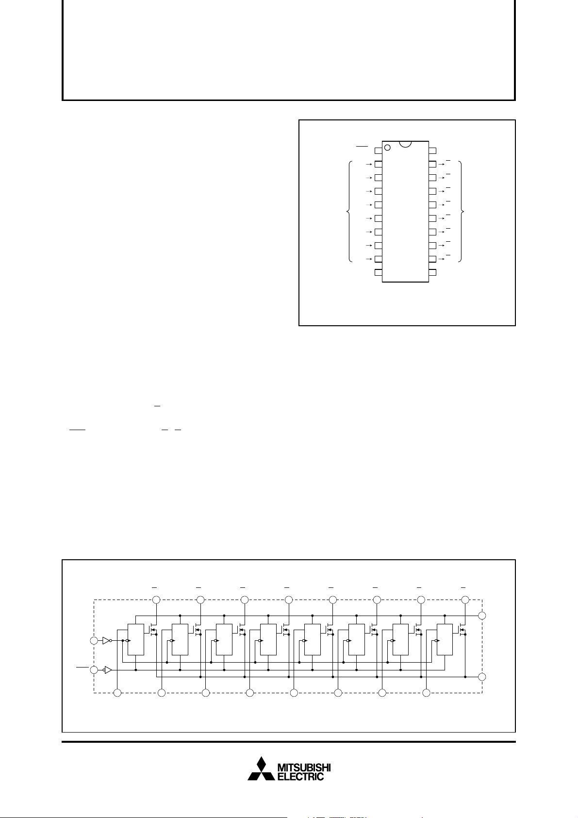
M81016 is octal D-type flip-flop driver by 20-pin package. It
has 8 same circuit units which is composed of D-type flip-flop
logic circuit and high voltage NchMOS output transistor.
M81016 has a common direct clear input and a common
clock input.
FEATURES
●
Lineup with three packages
●
High breakdown voltage (BVDSX ≥ 40V)
●
Drain output current (IDS(max) = 200mA)
●
With input protection diodes
●
Pin assignment of input-output flow through
●
Wide operating temperature range (Ta = –40 to +85°C)
APPLICATION
LED drive
FUNCTION
The common direct clear input and common clock input are
connected to every circuit unit by the same way. Signal at the
D inputs is transferred to Y outputs by D-type flip-flops on the
positive-going edge of the clock pulse.
If CLR is set to “L”, outputs Y1-Y8 will be altogether set to “H”
regardless of D1-D8 and CLK.
The maximum drain current of an output is 200mA. The
maximum between drain-source is 40V.
Moreover, M81016FP/KP can save space with mini-flat
package.
PIN CONFIGURATION (TOP VIEW)
1
CLR
2
D1
3
D2
4
D3
5
D4
INPUT OUTPUT
D5
D6
D7
D8
CLK
6
7
8
9
10
20
19
18
17
16
15
14
13
12
11
Package type 20P4B(P)
20P2N-A(FP)
20P2E-A(KP)
DD
V
Y1
Y2
Y3
Y4
Y5
Y6
Y7
Y8
GND
LOGIC DIAGRAM (POSITIVE LOGIC)
Y2
18
D
Q
CK
R
CLK
CLR
Y1
19
D
Q
D1
CK
R
2
D2
3
10
1
D3
Y3
17
D
Q
CK
R
4
D4
5
Y4
16
D
Q
CK
R
6
D5
Y5
15
D
Q
CK
R
7
D6
Y6
14
D
Q
CK
R
8
D7
Y7
13
D
Q
CK
R
9
D8
Y8
12
V
DD
20
D
Q
CK
R
11
GND
Oct.2004
Page 2
MITSUBISHI SEMICONDUCTOR <MOS-ARRAY>
M81016P/FP/KP
OCTAL D-TYPE FLIP-FLOP DRIVER WITH CLEAR
FUNCTION TABLE (EACH CHANNEL)
CLR
L
H
H
H
H
H : High level
L : Low level
INPUT
CLK
X
↑
↑
L
↓
D
X
L
H
X
X
OUTPUT : Y
H
H
L
Latched
Latched
TIMING DIAGRAM
CLK
D
CLR
X : Irrelevant
Y
ABSOLUTE MAXIMUM RATINGS (Unless otherwise noted, Ta = –40 ~ +85°C)
Symbol Parameter Conditions Unit
VDD
VDS
VI
IDS
Pd
Topr
Tstg
Supply voltage
Drain-to-source voltage
Input voltage
Drain output current
Power dissipation
Operating temperature
Storage temperature
Output, H
Current per circuit output, L
Ta = 25°C,
when mounted on board
M81016P
M81016FP
M81016KP
Ratings
7
–0.5 ~ +40
–0.5 ~ V
DD
200
1.47
1.10
0.68
–40 ~ +85
–55 ~ +125
V
V
V
mA
W
°C
°C
5V
GND
5V
GND
5V
GND
OH
V
V
OL
RECOMMENDED OPERATING CONDITIONS (Unless otherwise noted, Ta = –40 ~ +85°C)
Symbol
VDD
VDS
VIH
VIL
IDS
VIN
tr,t f
tsu
th
tw
f
Supply voltage
Drain-to-source voltage
“H” input voltage
“L” input voltage
Drain output current (Current per
1 circuit when 8 circuits are coming on simultaneously)
Input voltage
Rise time, Fall time, drain output
Setup time before CLK
Hold time, data after CLK
Pulse duration
Clock frequency
Parameter
Conditions
P
FP
KP
Duty Cycle no more than 45%
Duty Cycle no more than 100%
Duty Cycle no more than 34%
Duty Cycle no more than 100%
Duty Cycle no more than 18%
Duty Cycle no more than 100%
VDD = 4.5V
↑
↑
VDD = 4.5V
VDD = 4.5V
VDD = 4.5V
VDD = 4.5V
Limits
min typ max
DD
5.0
—
—
—
—
—
—
—
—
—
—
—
—
—
—
—
4.5
0
0.7V
0
0
0
0
0
0
0
0
0
20
5
40
—
5.5
40
DD
V
0.3VDD
200
135
200
120
200
95
VDD
500
—
—
—
20
Unit
V
V
V
V
mA
V
ns
ns
ns
ns
MHz
Oct.2004
Page 3
MITSUBISHI SEMICONDUCTOR <MOS-ARRAY>
OCTAL D-TYPE FLIP-FLOP DRIVER WITH CLEAR
ELECTRICAL CHARACTERISTICS (Unless otherwise noted, VDD = 5V, Ta = 25°C)
Symbol UnitParameter Test conditions
(BR)DSX
V
IDSX
IIH
IIL
ICC
VDS
RDS(on)
SWITCHING CHARACTERISTICS (VDD = 5V, Ta = 25°C)
Symbol UnitParameter Test conditions
TLH
t
tTHL
tPLH
tPHL
PLH(R)
t
Drain-source breakdown voltage
Drain-source leakage current
“H” input current
“L” input current
Supply current
“L” output voltage
Drain-source on-state resistance
Low-level to high-level and high-level to
low-level output transition time
Low-level to high-level and high-level to
low-level output propagation time (CLK)
Low-level to high-level output propagation
time (CLR)
DS = 1mA
I
V
DS = 40V
VDD = 5.5V, VI = 5.5V
VDD = 5.5V, VI = 0V
VDD = 5.5V
VI = 5.5V or 0V
IDS = 100mA, VDD = 4.5V
IDS = 200mA, VDD = 4.5V
IDS = 100mA, VDD = 4.5V
CL = 30pF (Note 1)
All outputs off
All outputs on
M81016P/FP/KP
Limits
min typ max
40
—
—
—
—
—
—
—
—
min typ max
—
—
—
—
—
—
0.002
0.005
0.005
0.005
0.005
0.25
0.51
Limits
10
35
30
35
2.5
3
—
5
1
–1
5
5
0.38
0.77
3.8
—
—
—
—
—
V
µA
µA
µA
µA
V
Ω
ns
ns
ns
ns
ns
Oct.2004
Page 4

NOTE 1 TEST CIRCUIT
PG
PG
CLR
D
CLK
VDD VCC
V
DD
Y
GND
MITSUBISHI SEMICONDUCTOR <MOS-ARRAY>
M81016P/FP/KP
OCTAL D-TYPE FLIP-FLOP DRIVER WITH CLEAR
R
L
(1) Pulse generator (PG) characteristics : PRR = 1MHz,
Duty Cycle = 50%, t
OUTPUT
(2) Output conditions : R
(3) Electrostatic capacity CL includes floating capacitance
at connections and input capacitance at probes.
L
C
r = 6ns, tf = 6ns, Zo = 50Ω, VI = 5V
L = 240Ω, VCC = 24V, VDD = 5V
TIMING DIAGRAM
CLK
CLK
5V
D
GND
5V
50%
50%
GND
t
10%
t
TLH
50%
PLH
90%
V
CC
V
OL
t
PHL
90%
Y
t
THL
50%
10%
SWITCHING TIMES
t
r
90%
90%
50%
10%
t
w
D
50%
t
su
h
t
50%
50%
t
f
10%
5V
GND
5V
GND
INPUT SETUP AND HOLD WAVEFORMS
Oct.2004
Page 5

TYPICAL CHARACTERISTICS
MITSUBISHI SEMICONDUCTOR <MOS-ARRAY>
M81016P/FP/KP
OCTAL D-TYPE FLIP-FLOP DRIVER WITH CLEAR
THERMAL DERATING FACTOR
2.0
1.5
CHARACTERISTICS
M81016P
M81016FP
1.0
M81016KP
0.5
0.764
0.572
0.354
POWER DISSIPATION Pd (W)
0
0 25 50 75 85 100
AMBIENT TEMPERATURE Ta (°C)
DUTY CYCLE-DRAIN CURRENT
CHARACTERISTICS
200 q~u
(M81016P)
160
120
DRAIN-SOURCE ON-STATE RESISTANCE
VS DRAIN CURRENT CHARACTERISTICS
5
DD=4.5V
V
4
Ta=85°C
3
Ta=25°C
Ta=–40°C
2
1
RESISTANCE RDS(ON) (Ω)
DRAIN-SOURCE ON-STATE
0
110
1
10
DRAIN CURRENT I
2
2 10
DS (mA)
3
35723 5723 57
DUTY CYCLE-DRAIN CURRENT
CHARACTERISTICS
i
200
(M81016P)
q~e
r
t
160
y
u
i
120
80
•
The drain
current values represent
the current per circuit.
•
40
Repeated frequency ≥ 10Hz
DRAIN CURRENT IDS (mA)
•
The value the circle represents the
value of the simultaneously-operated circuit.
•
Ta=25°C
0
080604020 100
DUTY CYCLE (%)
DUTY CYCLE-DRAIN CURRENT
CHARACTERISTICS
200
(M81016FP)
160
120
80
•
The drain
current values represent
the current per circuit.
•
Repeated frequency ≥ 10Hz
40
DRAIN CURRENT IDS (mA)
•
The value the circle represents the
value of the simultaneously-operated circuit.
•
Ta=25°C
0
080604020 100
q~t
y
u
i
80
•
The drain
current values represent
the current per circuit.
•
Repeated frequency ≥ 10Hz
40
DRAIN CURRENT IDS (mA)
•
The value the circle represents the
value of the simultaneously-operated circuit.
•
Ta=85°C
0
080604020 100
DUTY CYCLE (%)
DUTY CYCLE-DRAIN CURRENT
CHARACTERISTICS
200
(M81016FP)
160
120
80
•
The drain
current values represent
the current per circuit.
•
Repeated frequency ≥ 10Hz
40
•
The value the circle represents the
DRAIN CURRENT IDS (mA)
value of the simultaneously-operated circuit.
•
Ta=85°C
0
080604020 100
q~w
e
r
t
y
u
i
DUTY CYCLE (%)
DUTY CYCLE (%)
Oct.2004
Page 6

MITSUBISHI SEMICONDUCTOR <MOS-ARRAY>
M81016P/FP/KP
OCTAL D-TYPE FLIP-FLOP DRIVER WITH CLEAR
DUTY CYCLE-DRAIN CURRENT
CHARACTERISTICS
200
(M81016KP)
160
(mA)
DS
120
80
•
The drain
current values represent
the current per circuit.
•
Repeated frequency ≥ 10Hz
40
DRAIN CURRENT I
•
The value the circle represents the
value of the simultaneously-operated circuit.
•
Ta=25°C
0
080604020 100
DUTY CYCLE (%)
SWITCHING TIME-AMBIENT TEMPERATURE
CHARACTERISTICS
L
=240Ω,V
R
CC
=24V,VDD=5V VCC=24V,V
t
PLH,tPLH(R)
t
PHL
(ns)
50
40
30
20
t
t
TLH
THL
80–20–40 4020 100060
SWITCHING TIME
10
0
q~e
r
t
y
u
i
DUTY CYCLE-DRAIN CURRENT
CHARACTERISTICS
200
(M81016KP)
160
(mA)
DS
120
80
•
The drain
current values represent
the current per circuit.
•
Repeated frequency ≥ 10Hz
40
•
DRAIN CURRENT I
The value the circle represents the
value of the simultaneously-operated circuit.
•
Ta=85°C
0
080604020 100
DUTY CYCLE (%)
SWITCHING TIME-DRAIN CURRENT
3
10
7
5
3
2
(ns)
2
10
7
5
3
2
1
10
7
5
SWITCHING TIME
3
2
0
10
10
CHARACTERISTICS
DD
=5V,Ta=25°C
TLH
t
t
PLH
t
PHL
t
THL
1
2
335577
10
2
2
10
q
w
e
r
t
y
u
i
3
AMBIENT TEMPERATURE Ta
(°C)
DRAIN CURRENT I
DS
(mA)
Oct.2004
Page 7

MITSUBISHI SEMICONDUCTOR <MOS-ARRAY>
M81016P/FP/KP
OCTAL D-TYPE FLIP-FLOP DRIVER WITH CLEAR
20P4B
EIAJ Package Code
SDIP20-P-300-1.78
SEATING PLANE
JEDEC Code
–
20
1
LA
Weight(g)
1.0
D
e
b
Lead Material
Alloy 42/Cu Alloy
11
10
1
b
c
E
Symbol
2
A
1
A
A
A
1
2
A
b
b
1
c
D
E
e
e
1
L
1
e
Dimension in Millimeters
Min Nom Max
––4.5
0.51 – –
– 3.3 –
0.38 0.48 0.58
0.9 1.0 1.3
0.22 0.27 0.34
18.8 19.0 19.2
6.15 6.3 6.45
– 1.778 –
–7.62–
3.0 – –
0° –15°
Plastic 20pin 300mil SDIP
20P2N-A
EIAJ Package Code
SOP20-P-300-1.27
E
E
H
G
Z
JEDEC Code
–
20 11
1
Weight(g)
D
e
z
1
Detail G
y
0.26
Cu Alloy
1
e
10
F
A
Symbol
A
A
1
A
2
b
c
D
Lead Material
A
b
x
M
2
A
1
E
e
H
E
L
1
L
z
Z
1
L
L
c
Detail F
1
x
y
b
2
e
1
I
2
e
b
2
Recommended Mount Pad
Dimension in Millimeters
Min Nom Max
–
0
–
–
–
–
–
–
–
–
.10
.81
.40
.350
.20
.180
.612
.512
.35
.25
.271
.87
.57
.60
.40
.251
0.585
–
–
–
0° – 8°
– .760 –
–
.627
–
.271
2
I
.12
.20
–
.50
.250
.712
.45
–
.18
.80
–
–
0.735
0.25
.10
–
–
Plastic 20pin 300mil SOP
Oct.2004
Page 8

MITSUBISHI SEMICONDUCTOR <MOS-ARRAY>
M81016P/FP/KP
OCTAL D-TYPE FLIP-FLOP DRIVER WITH CLEAR
20P2E-A
EIAJ Package Code
SSOP20-P-225-0.65
HE
G
JEDEC Code
20 11
E
1
e
Z1
z
–
D
y
Detail G
10
b
Weight(g)
0.08
x
M
Lead Material
Alloy 42
A
A
2 A1
L1
Detail F
Plastic 20pin 225mil SSOP
e
b2
e1
F
L
c
Recommended Mount Pad
Symbol
Dimension in Millimeters
Min Nom Max
A
A1
A
H
L
Z1
b
e1
–
0
2
–
.170
b
.130
c
D
.46
E
.34
e
–
.26
E
.30
L
–
1
z
–
–
x
–
y
–
0° – 10°
2
– .350 –
–
I2
.01
–
.10
.151
.220
.150
.56
.44
.650
.46
.50
.01
0.325
–
–
–
.85
–
I2
.451
.20
–
.320
.20
.66
.54
–
.66
.70
–
–
0.475
0.13
.10
–
–
Oct.2004
 Loading...