

MITSUBISHI LSIs
M6MGB/T166S2BWG
16,777,216-BIT (1,048,576 -WORD BY 16-BIT ) CMOS
3.3V-ONLY FLASH MEMORY &
2,097,152-BIT (131,072-WORD BY 16-BIT) CMOS SRAM
Stacked-CSP (Chip Scale Package)
DESCRIPTION
The MITSUBISHI M6MGB/T166S2BWG is a Stacked Chip
Scale Package (S-CSP) that contents 16M-bits flash
memory and 2M-bits Static RAM in a 72-pin S-CSP.
16M-bits Flash memory is a 1,048,576 words, 3.3V-only,
and high performance non-volatile memory fabricated by
CMOS technology for the peripheral circuit and
DINOR(DIvided bit-line NOR) architecture for the memory
cell.
2M-bits SRAM is a 131,072words unsynchronous SRAM
fabricated by silicon-gate CMOS technology.
M6MGB/T166S2BWG is suitable for the application of the
mobile-communication-system to reduce both the mount
space and weight .
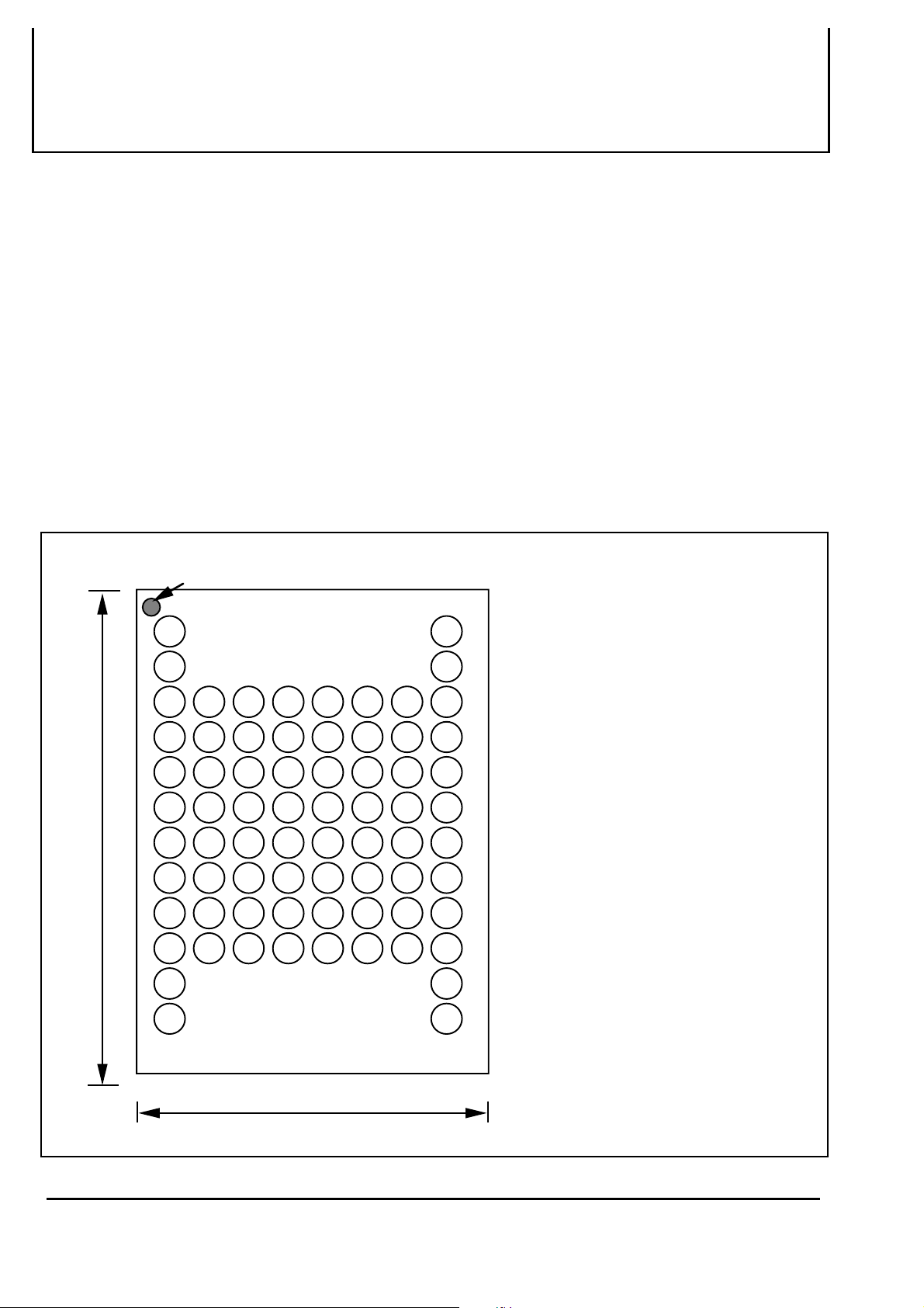
PIN CONFIGURATION (TOP VIEW)
INDEX (Laser Marking)
1
2345678
NC
A
FEATURES
• Access time
Flash Memory 90ns (Max.)
SRAM 85ns (Max.)
• Supply voltage Vcc=2.7 ~ 3.6V
• Ambient temperature
I version Ta=-40 ~ 85°C
• Package : 72-pin S-CSP , 0.8mm ball pitch
APPLICATION
Mobile communication products
NC
B
C
D
E
F
G
11.0 mm
H
I
J
K
L
NC
DU
A5
A4
A0
F-CE#
F-GND
F-OE#
DU
NC
NC
F-A18
F-A17
A7
A6
A3
A2
A1
SCE1#
S-LB#
S-UB#
S-OE#
DU
DQ9
DQ8
DQ0
DQ1
F-WP#
NC
F-A19
DQ11
DU
DQ10
DQ2
DQ3
8.0 mm
GND
F-RP#
DU
DU
DQ12
SCE2
S-VCC
F-VCC
F-WE#
F-
RY/BY#
DU
NC
DQ13
DQ6
DQ4
DQ5
A16
A8
A10
A9
DQ15
S-WE#
DQ14
DQ7
NC
NC
A11
A15
A14
A13
A12
F-GND
DU
NC
NC
F-VCC
S-VCC
:Vcc for Flash
:Vcc for SRAM
F-GND :GND for Flash
GND :Flash/SRAM common GND
A0-A16
:Flash/SRAM
common Address
F-A17-F-A19
DQ0-DQ15
:Address for Flash
:Flash/SRAM
common Data I/O
F-CE# :Flash Chip Enable
S-CE1#
S-CE2
:SRAM Chip Enable 1
:SRAM Chip Enable 2
F-OE# :Flash Output Enable
S-OE# :SRAM Output Enable
F-WE#
S-WE#
:Flash Write Enable
:SRAM Write Enable
F-WP# :Flash Write Protect
F-RP# :Flash Reset Power Down
F-RY/BY# :Flash Ready /Busy
S-LB#
S-UB#
NC:Non Connection
DU:Don't Use (Note: Should be open)
:SRAM Lower Byte
:SRAM Upper Byte
1
Nov 1999 , Rev.2.3

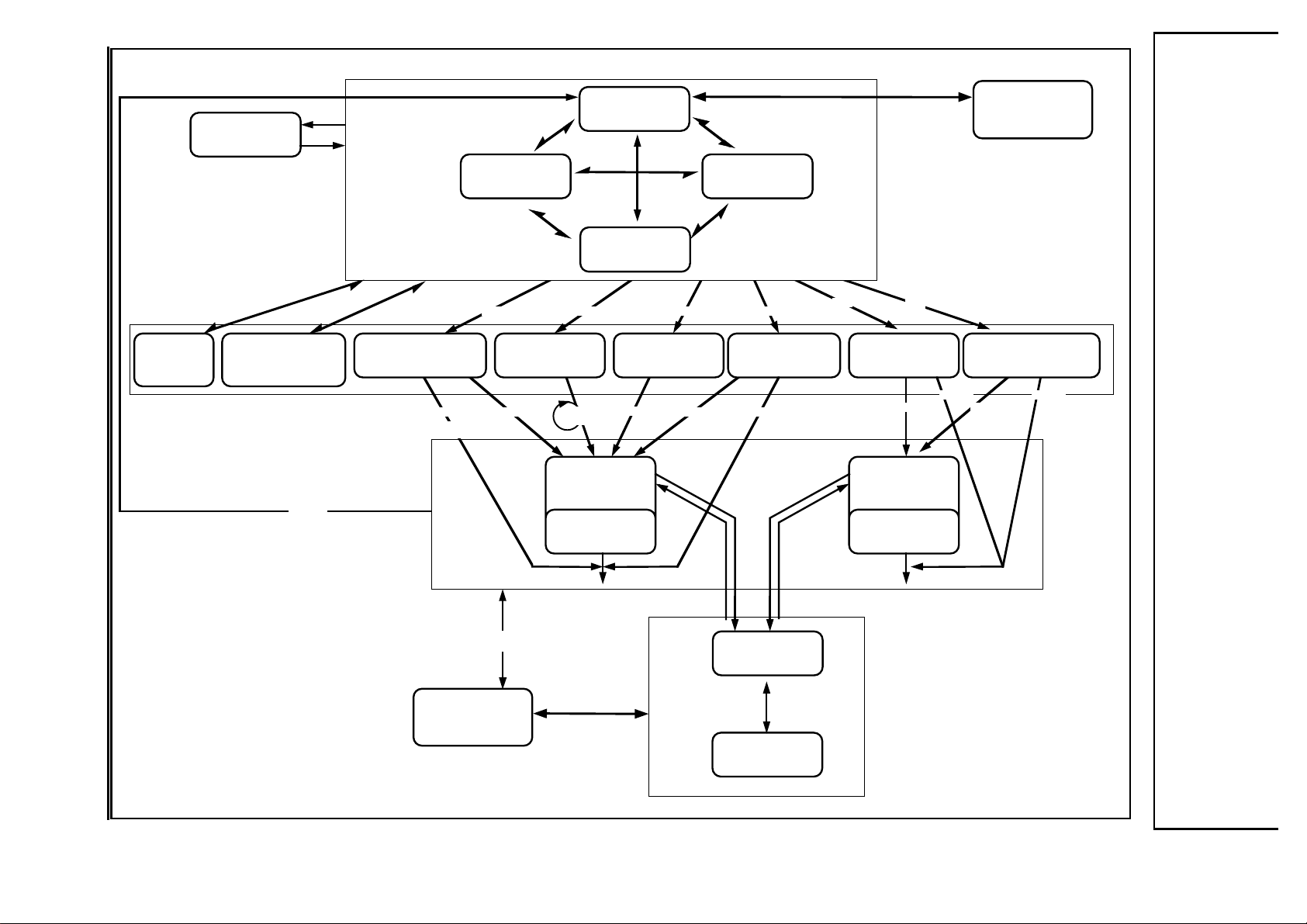
BLOCK DIAGRAM
MITSUBISHI LSIs
M6MGB/T166S2BWG
16,777,216-BIT (1,048,576 -WORD BY 16-BIT ) CMOS
3.3V-ONLY FLASH MEMORY &
2,097,152-BIT (131,072-WORD BY 16-BIT) CMOS SRAM
Stacked-CSP (Chip Scale Package)
16Mb Flash Memory
ADDRESS
INPUTS
FLASH CHIP ENABLE INPUT
FLASH OUTPUT ENABLE INPUT
FLASH WRITE ENABLE INPUT
FLASH WRITE PROTECT INPUT
FLASH RESET/POWER DOWN INPUT
FLASH READY/BUSY OUTPUT
2Mb SRAM
F-A19
F-A18
F-A17
A16
A15
A14
A13
A12
A11
A10
A9
A8
A7
A6
A5
A4
A3
A2
A1
A0
F-CE#
F-OE#
F-WE#
F-WP#
F-RP#
F-RY/BY#
X-DECODER
Y-DECODER
STATUS / ID REGISTER
WSM
CUI
WSM
128 WORD PAGE BUFFER
Main Block 32KW
Bank(II)
28
Main Block 32KW
Parameter Block7 16KW
Parameter Block6 16KW
Bank(I)
Parameter Block5 16KW
Parameter Block4 16KW
Parameter Block3 16KW
Parameter Block2 16KW
Parameter Block1 16KW
Boot Block 16KW
Y-GATE / SENSE AMP.
MULTIPLEXER
INPUT/OUTPUT
BUFFERS
DQ15
DQ14DQ13DQ12 DQ2DQ1DQ0DQ3
DATA INPUTS/OUTPUTS
F-VCC
F-GND/GND
A0
A1
A15
A16
S-CE1#
S-CE2
S-LB#
S-UB#
S-WE#
S-OE#
131072 WORD x
16 BITS
ROW DECODER
ADDRESS INPUT BUFFER
GENERATOR
CLOCK
SENSE AMP.
SENSE AMP.
DATAINPUT
DATAINPUT
OUTPUT BUFFER
OUTPUT BUFFER
BUFFER
BUFFER
DQ0
DQ7
DQ
8
15
DQ
S-VCC
GND
2
Nov 1999 , Rev.2.3
MITSUBISHI LSIs
M6MGB/T166S2BWG
16,777,216-BIT (1,048,576 -WORD BY 16-BIT ) CMOS
3.3V-ONLY FLASH MEMORY &
2,097,152-BIT (131,072-WORD BY 16-BIT) CMOS SRAM
Stacked-CSP (Chip Scale Package)
1. Flash Memory
DESCRIPTION
The Flash Memory of M6MGB/T166S2BWG is 3.3V-only high speed 16,777,216-bit CMOS boot block Flash Memories with alternating
BGO (Back Ground Operation) feature. The BGO feature of the device allows Program or Erase operations to be performed in one bank
while the device simultaneously allows Read operations to be performed on the other bank. This BGO feature is suitable for mobile and
personal computing, and communication products. The Flash Memory of M6MGB/T166S2BWG is fabricated by CMOS technology for the
peripheral circuits and DINOR(Divided bit line NOR) architecture for the memory cells.
FEATURES
Organization 1048,576 word x 16bit
Supply voltage
Access time 90ns (Max.)
Power Dissipation
Read 54 mW (Max. at 5MHz)
(After Automatic Power Down) 0.33mW (typ.)
Program/Erase 126 mW (Max.)
Standby 0.33mW (typ.)
Deep power down mode 0.33mW (typ.)
Auto program for Bank(I)
Program Time 4ms (typ.)
Program Unit
(Byte Program) 1word
(Page Program) 128word
Auto program for Bank(II)
Program Time 4ms (typ.)
Program Unit 128word
Auto Erase
Erase time 40 ms (typ.)
Erase Unit
Bank(I) Boot Block 16Kword x 1
Parameter Block 16Kword x 7
Bank(II) Main Block 32Kword x 28
Program/Erase cycles 100Kcycles
.................................
.............................
................................ VCC = 2.7~3.6V
..............................
.................................
..........
.................................
.................................
.......................
.................................
.........................
.........................
.................................
.................................
.................................
.....................
..............
......................
.........................................
Boot Block
M6MGB166S2BWG Bottom Boot
M6MGT166S2BWG Top Boot
Other Functions
Soft Ware Command Control
Selective Block Lock
Erase Suspend/Resume
Program Suspend/Resume
Status Register Read
Alternating Back Ground Program/Erase Operation
Between Bank(I) and Bank(II)
Auto Power Down Mode
........................
........................
3
Nov 1999 , Rev.2.3

MITSUBISHI LSIs
M6MGB/T166S2BWG
16,777,216-BIT (1,048,576 -WORD BY 16-BIT ) CMOS
3.3V-ONLY FLASH MEMORY &
2,097,152-BIT (131,072-WORD BY 16-BIT) CMOS SRAM
Stacked-CSP (Chip Scale Package)
FUNCTION
The Flash Memory of M6MGB/T166S2BWG includes on-chip
program/erase control circuitry. The Write State Machine (WSM)
controls block erase and byte/page program operations.
Operational modes are selected by the commands written to the
Command User Interface (CUI). The Status Register indicates the
status of the WSM and when the WSM successfully completes the
desired program or block erase operation.
A Deep Powerdown mode is enabled when the F-RP# pin is at
GND, minimizing power consumption.
Read
The Flash Memory of M6MGB/T166S2BWG has three read
modes, which accesses to the memory array, the Device Identifier
and the Status Register. The appropriate read command are
required to be written to the CUI. Upon initial device powerup or
after exit from deep powerdown, the Flash Memory automatically
resets to read array mode. In the read array mode, low level input
to F-CE# and F-OE#, high level input to F-WE# and F-RP#, and
address signals to the address inputs (F-A19-F-A17,A16-A0)
output the data of the addressed location to the data input/output (
D15-D0).
Write
Writes to the CUI enables reading of memory array data, device
identifiers and reading and clearing of the Status Register. They
also enable block erase and program. The CUI is written by
bringing F-WE# to low level, while F-CE# is at low level and F-OE#
is at high level. Address and data are latched on the earlier rising
edge of F-WE# and F-CE#. Standard micro-processor write
timings are used.
Deep Power-Down
When F-RP# is at VIL, the device is in the deep powerdown
mode and its power consumption is substantially low. During
read modes, the memory is deselected and the data
input/output are in a high-impedance(High-Z) state. After
return from powerdown, the CUI is reset to Read Array , and
the Status Register is cleared to value 80H.
During block erase or program modes, F-RP# low will abort
either operation. Memory array data of the block being altered
become invalid.
Automatic Power-Down (APD)
The Automatic Power-Down minimizes the power
consumption during read mode. The device automatically
turns to this mode when any addresses or F-CE# isn't
changed more than 200ns after the last alternation. The
power consumption becomes the same as the stand-by
mode. While in this mode, the output data is latched and can
be read out. New data is read out correctly when addresses
are changed.
Alternating Background Operation (BGO)
The Flash Memory of M6MGB/T166S2BWG allows to read array
from one bank while the other bank operates in software
command write cycling or the erasing / programming operation in
the background. Read array operation with the other bank in BGO
is performed by changing the bank address without any additional
command. When the bank address points the bank in software
command write cycling or the erasing / programming operation,
the data is read out from the status register. The access time with
BGO is the same as the normal read operation.
Output Disable
When F-OE# is at VIH, output from the devices is disabled. Data
input/output are in a high-impedance(High-Z) state.
Standby
When F-CE# is at VIH, the device is in the standby mode and
its power consumption is reduced. Data input/output are in a
high-impedance(High-Z) state. If the memory is deselected
during block erase or program, the internal control circuits
remain active and the device consume normal active power
until the operation completes.
4
Nov 1999 , Rev.2.3

MITSUBISHI LSIs
M6MGB/T166S2BWG
16,777,216-BIT (1,048,576 -WORD BY 16-BIT ) CMOS
3.3V-ONLY FLASH MEMORY &
2,097,152-BIT (131,072-WORD BY 16-BIT) CMOS SRAM
Stacked-CSP (Chip Scale Package)
SOFTWARE COMMAND DEFINITIONS
The device operations are selected by writing specific software
command into the Command User Interface.
Read Array Command (FFH)
The device is in Read Array mode on initial device power up and
after exit from deep powerdown, or by writing FFH to the
Command User Interface. After starting the internal operation the
device is set to the read status register mode automatically.
Read Device Identifier Command (90H)
It can normally read device identifier codes when Read Device
Identifier Code Command(90H) is written to the command latch.
Following the command write, the manufacturer code and the
device code can be read from address 00000H and 00001H,
respectively.
Read Status Register Command (70H)
The Status Register is read after writing the Read Status Register
command of 70H to the Command User Interface. Also, after
starting the internal operation the device is set to the Read Status
Register mode automatically.
The contents of Status Register are latched on the later falling
edge of F-OE# or F-CE#. So F-CE# or F-OE# must be toggled
every status read.
Clear Status Register Command (50H)
The Erase Status, Program Status and Block Status bits are set to
"1"s by the Write State Machine and can only be reset by the Clear
Status Register command of 50H. These bits indicates various
failure conditions.
C)Single Data Load to Page Buffer (74H)
/ Page Buffer to Flash (0EH/D0H)
Single data load to the page buffer is performed by writing 74H
followed by a second write specifying the column address and
data. Distinct data up to 128word can be loaded to the page
buffer by this two-command sequence. On the other hand, all of
the loaded data to the page buffer is programed simultaneously
by writing Page Buffer to Flash command of 0EH followed by the
confirm command of D0H. After completion of programing the
data on the page buffer is cleared automatically.
This command is valid for only Bank(I) alike Word/Byte Program.
Clear Page Buffer Command (55H)
Loaded data to the page buffer is cleared by writing the Clear
Page Buffer command of 55H followed by the Confirm command
of D0H. This command is valid for clearing data loaded by Single
Data Load to Page Buffer command.
Suspend/Resume Command (B0H/D0H)
Writing the Suspend command of B0H during block erase
operation interrupts the block erase operation and allows read out
from another block of memory. Writing the Suspend command of
B0H during program operation interrupts the program operation
and allows read out from another block of memory. The Bank
address is required when writing the Suspend/Resume Command.
The device continues to output Status Register data when read,
after the Suspend command is written to it. Polling the WSM
Status and Suspend Status bits will determine when the erase
operation or program operation has been suspended. At this
point, writing of the Read Array command to the CUI enables
reading data from blocks other than that which is suspended.
When the Resume command of D0H is written to the CUI,
the WSM will continue with the erase or program processes.
Block Erase / Confirm Command (20H/D0H)
Automated block erase is initiated by writing the Block Erase
command of 20H followed by the Confirm command of D0H. An
address within the block to be erased is required. The WSM
executes iterative erase pulse application and erase verify
operation.
Program Commands
A)Word Program (40H)
Word program is executed by a two-command sequence. The
Word Program Setup command of 40H is written to the
Command Interface, followed by a second write specifying the
address and data to be written. The WSM controls the program
pulse application and verify operation. The Word Program
Command is valid for only Bank(I).
B)Page Program for Data Blocks (41H)
Page Program for Bank(I) and Bank(II) allows fast programming of
128words of data. Writing of 41H initiates the page program
operation for the Data area. From 2nd cycle to 129th cycle, write
data must be serially inputted. Address A6-A0 have to be
incremented from 00H to 7FH. After completion of data loading, the
WSM controls the program pulse application and verify operation.
DATA PROTECTION
The Flash Memory of M6MGB/T166S2BWG provides selectable
block locking of memory blocks. Each block has an associated
nonvolatile lock-bit which determines the lock status of the block.
In addition, the Flash Memory has a master Write Protect pin
(F-WP#) which prevents any modifications to memory blocks
whose lock-bits are set to "0", when F-WP# is low. When F-WP#
is high, all blocks can be programmed or erased regardless of
the state of the lock-bits, and the lock-bits are cleared to "1" by
erase. See the BLOCK LOCKING table on P.9 for details.
Power Supply Voltage
When the power supply voltage (F-VCC) is less than V
V
CC Lock-Out voltage, the device is set to the Read-only mode.
Regarding DC electrical characteristics of V
A delay time of 2ms is required before any device operation is
initiated. The delay time is measured from the time F-Vcc reaches
F-Vccmin (2.7V).
During power up, F-RP#=GND is recommended. Falling in Busy
status is not recommended for possibility of damaging the device.
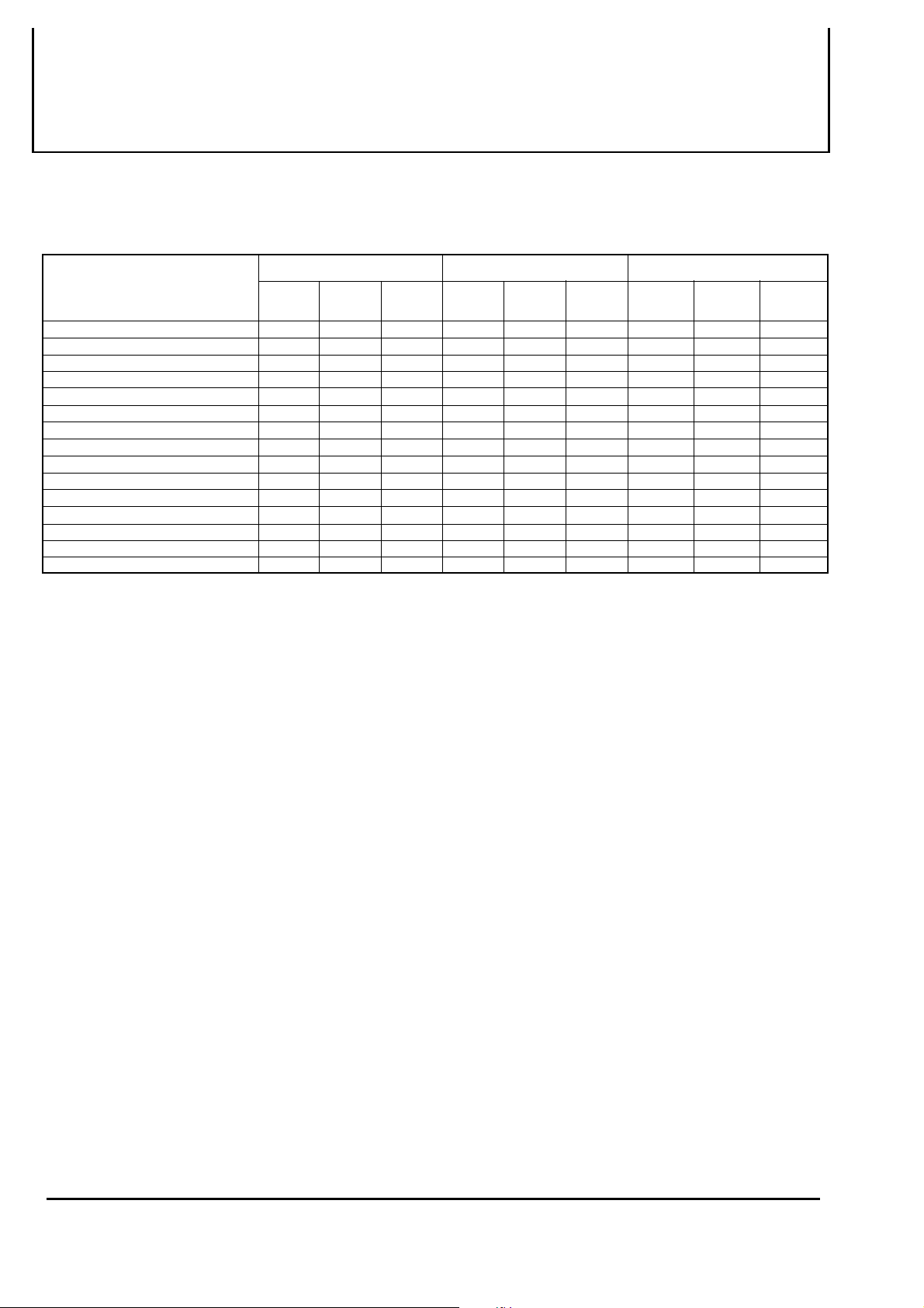
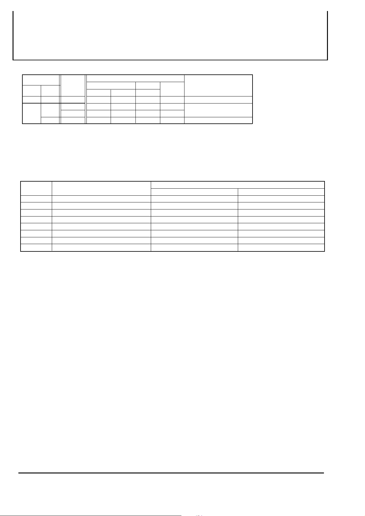
MEMORY ORGANIZATION
The Flash Memory of M6MGB/T166S2BWG has one 16Kword
boot block, seven 16Kword parameter blocks, for Bank(I) and
twenty-eight 32Kword main blocks for Bank(II). A block is erased
independently of other blocks in the array.
LKO, see P.10.
LKO, Low
5
Nov 1999 , Rev.2.3
MEMORY ORGANIZATION
MITSUBISHI LSIs
M6MGB/T166S2BWG
16,777,216-BIT (1,048,576 -WORD BY 16-BIT ) CMOS
3.3V-ONLY FLASH MEMORY &
2,097,152-BIT (131,072-WORD BY 16-BIT) CMOS SRAM
Stacked-CSP (Chip Scale Package)
F8000H-FFFFFH
F0000H-F7FFFH
E8000H-EFFFFH
E0000H-E7FFFH
D8000H-DFFFFH
D0000H-D7FFFH
C8000H-CFFFFH
C0000H-C7FFFH
B8000H-BFFFFH
B0000H-B7FFFH
A8000H-AFFFFH
A0000H-A7FFFH
98000H-9FFFFH
90000H-97FFFH
88000H-8FFFFH
80000H-87FFFH
78000H-7FFFFH
70000H-77FFFH
68000H-6FFFFH
60000H-67FFFH
58000H-5FFFFH
50000H-57FFFH
48000H-4FFFFH
40000H-47FFFH
38000H-3FFFFH
30000H-37FFFH
28000H-2FFFFH
20000H-27FFFH
1C000H-1FFFFH
18000H-1BFFFH
14000H-17FFFH
10000H-13FFFH
0C000H-0FFFFH
08000H-0BFFFH
04000H-07FFFH
00000H-03FFFH
F-A19-F-A17,A16-A0
32Kword MAIN BLOCK 35
32Kword MAIN BLOCK 34
32Kword MAIN BLOCK 33
32Kword MAIN BLOCK 32
32Kword MAIN BLOCK 31
32Kword MAIN BLOCK 30
32Kword MAIN BLOCK 29
32Kword MAIN BLOCK 28
32Kword MAIN BLOCK 27
32Kword MAIN BLOCK 26
32Kword MAIN BLOCK 25
32Kword MAIN BLOCK 24
32Kword MAIN BLOCK 23
32Kword MAIN BLOCK 22
32Kword MAIN BLOCK 21
32Kword MAIN BLOCK 20
32Kword MAIN BLOCK 19
32Kword MAIN BLOCK 18
32Kword MAIN BLOCK 17
32Kword MAIN BLOCK 16
32Kword MAIN BLOCK 15
32Kword MAIN BLOCK 14
32Kword MAIN BLOCK 13
32Kword MAIN BLOCK 12
32Kword MAIN BLOCK 11
32Kword MAIN BLOCK 10
32Kword MAIN BLOCK 9
32Kword MAIN BLOCK 8
16Kword PARAMETER BLOCK 7
16Kword PARAMETER BLOCK 6
16Kword PARAMETER BLOCK 5
16Kword PARAMETER BLOCK 4
16Kword PARAMETER BLOCK 3
16Kword PARAMETER BLOCK 2
16Kword PARAMETER BLOCK 1
16Kword BOOT BLOCK 0
Flash Memory of M6MGB166S2BWG
Memory Map
BANK(II)
BANK(I)
FC000H-FFFFFH
F8000H-FBFFFH
F4000H-F7FFFH
F0000H-F3FFFH
EC000H-EFFFFH
E8000H-EBFFFH
E4000H-E7FFFH
E0000H-E3FFFH
D8000H-DFFFFH
D0000H-D7FFFH
C8000H-CFFFFH
C0000H-C7FFFH
B8000H-BFFFFH
B0000H-B7FFFH
A8000H-AFFFFH
A0000H-A7FFFH
98000H-9FFFFH
90000H-97FFFH
88000H-8FFFFH
80000H-87FFFH
78000H-7FFFFH
70000H-77FFFH
68000H-6FFFFH
60000H-67FFFH
58000H-5FFFFH
50000H-57FFFH
48000H-4FFFFH
40000H-47FFFH
38000H-3FFFFH
30000H-37FFFH
28000H-2FFFFH
20000H-27FFFH
18000H-1FFFFH
10000H-17FFFH
08000H-0FFFFH
00000H-07FFFH
F-A19-F-A17,A16-A0
16Kword BOOT BLOCK 35
16Kword PARAMETER BLOCK 34
16Kword PARAMETER BLOCK 33
16Kword PARAMETER BLOCK 32
16Kword PARAMETER BLOCK 31
16Kword PARAMETER BLOCK 30
16Kword PARAMETER BLOCK 29
16Kword PARAMETER BLOCK 28
32Kword MAIN BLOCK 27
32Kword MAIN BLOCK 26
32Kword MAIN BLOCK 25
32Kword MAIN BLOCK 24
32Kword MAIN BLOCK 23
32Kword MAIN BLOCK 22
32Kword MAIN BLOCK 21
32Kword MAIN BLOCK 20
32Kword MAIN BLOCK 19
32Kword MAIN BLOCK 18
32Kword MAIN BLOCK 17
32Kword MAIN BLOCK 16
32Kword MAIN BLOCK 15
32Kword MAIN BLOCK 14
32Kword MAIN BLOCK 13
32Kword MAIN BLOCK 12
32Kword MAIN BLOCK 11
32Kword MAIN BLOCK 10
32Kword MAIN BLOCK 9
32Kword MAIN BLOCK 8
32Kword MAIN BLOCK 7
32Kword MAIN BLOCK 6
32Kword MAIN BLOCK 5
32Kword MAIN BLOCK 4
32Kword MAIN BLOCK 3
32Kword MAIN BLOCK 2
32Kword MAIN BLOCK 1
32Kword MAIN BLOCK 0
Flash Memory of M6MGT166S2BWG
Memory Map
BANK(I)
BANK(II)
6
Nov 1999 , Rev.2.3
BUS OPERATIONS
Bus Operations for Word-Wide Mode
MITSUBISHI LSIs
M6MGB/T166S2BWG
16,777,216-BIT (1,048,576 -WORD BY 16-BIT ) CMOS
3.3V-ONLY FLASH MEMORY &
2,097,152-BIT (131,072-WORD BY 16-BIT) CMOS SRAM
Stacked-CSP (Chip Scale Package)
Mode
Read
Pins
Array
Status Register
F-CE#
V
IL
VIL
F-OE#
VIL
VIL
Lock Bit Status VIL VIL
Identifier Code
Output disable
Stand by
Program
Write
Erase
Others
Deep Power Down
1) X at F-RY/BY# is VOL or VOH(Hi-Z).
*The F-RY/BY# is an open drain output pin and indicates status of the internal WSM. When low,it indicates that the WSM is Busy performing an operation.
A pull-up resistor of 10K-100K Ohms is required to allow the F-RY/BY# signal to transition high indicating a Ready WSM condition.
2) X can be V
IH or VIL for control pins.
VIL
VIL
VIH
VIL
VIL
V
IL VIH
X
VIL
VIH
V
VIH
2)
X
IH
X
F-WE#
VIH
VIH
VIH
VIH
VIH
X
IL
V
VIL
IL
V
X Hi-Z
F-RP#
IH
V
VIH
VIH
VIH
VIH
VIH
VIH
VIH
IH
V
VIL
Status Register Data
Lock Bit Data (DQ6)X
Command/Data in
DQ
0-15
Data out
Identifier Code
Hi-Z
Hi-Z
Command
F-RY/BY#
OH (Hi-Z)
V
X
V
OH (Hi-Z)
X
X
X
X
XCommand
VOH (Hi-Z)
1)
7
Nov 1999 , Rev.2.3
SOFTWARE COMMAND DEFINITION
Command List
MITSUBISHI LSIs
M6MGB/T166S2BWG
16,777,216-BIT (1,048,576 -WORD BY 16-BIT ) CMOS
3.3V-ONLY FLASH MEMORY &
2,097,152-BIT (131,072-WORD BY 16-BIT) CMOS SRAM
Stacked-CSP (Chip Scale Package)
1st bus cycle
Command
Mode
Address
Read Array
Device Identifier
Read Status Register
Clear Status Register
Clear Page Buffer
Word Program
Page Program
5)
7)
Single Data Load to Page Buffer
Page Buffer to Flash
5)
Block Erase / Confirm
Suspend
Resume
Read Lock Bit Status
Lock Bit Program / Confirm
Erase All Unlocked Blocks
1) Upper byte data (DQ8-DQ15) is ignored.
2) IA=ID Code Address : A0=VIL (Manufacturer's Code) : A0=VIH (Device Code), ID=ID Code
3) Bank = Bank Address (Bank(I) or Bank(II)) : F-A19-F-A17.
4) SRD = Status Register Data
5) Word Program, Single Data Load and Page Buffer to Flash Command is valid for only Bank(I).
6) WA = Write Address,WD = Write Data
7) WA0,WAn=Write Address, WD0,WDn=Write Data.
Write Address and Write Data must be provided sequentially from 00H to 7FH for A6-A0. Page size is 128word (128word x 16bit).
and also F-A19-F-A17,A16-A7(Block Address, Page Address) must be valid.
8) WA = Write Address : Upper page address, F-A19-F-A17,A16-A7(Block Address, Page Address) must be valid.
9) BA = Block Address : BA = Block Address : F-A19-F-A17,A16-A14(Bank1) F-A19-F-A17,A16-A15(Bank2)
10) DQ6 provides Block Lock Status, DQ6 = 1 : Block Unlock, DQ6 = 0 : Block Locked.
Write
Bank
XWrite
XWrite
Write 40H Write
Write 41H
5)
Write
Write
Write
Write
Write
Write
Write
Write
Bank(I)
Bank
Bank(I)
Bank(I)
Bank
Bank
Bank
X
Bank
X
3)
5)
5)
5)
Data
(DQ15-0)
FFHXWrite
90HX
70HWrite
50H
55H
74H
0EH
20H
B0H
D0H
71H
77H
A7H
2nd bus cycle
AddressMode
IARead
Bank
Data
(DQ15-0)
2)
ID
SRDRead
Write X D0H
6)
WD
7)
WD0
WDWA
8)
D0H
9)
D0H
DQ6
D0H
Write
Write
Write
Write
Read
Write
Write
WA
WA
BA
BA
BA
XD0H
3rd ~129th bus cycles (Word Mode)
AddressMode
2)
4)
1)
6)
7)
1)
1)
10)
1)
1)
WAnWA0
Data
(DQ15-0)
7)
7)
WDnWrite
8
Nov 1999 , Rev.2.3
MITSUBISHI LSIs
M6MGB/T166S2BWG
16,777,216-BIT (1,048,576 -WORD BY 16-BIT ) CMOS
3.3V-ONLY FLASH MEMORY &
2,097,152-BIT (131,072-WORD BY 16-BIT) CMOS SRAM
Stacked-CSP (Chip Scale Package)
BLOCK LOCKING
Lock
F-WP#
F-RP#
VIL
VIH
1) DQ6 provides Lock Status of each block after writing the Read Lock Status command (71H).
F-WP# pins must not be switched during performing Erase / Write operations or WSM Busy (WSMS = 0).
2) Erase/Write command for locked blocks is aborted. At this time read mode is not array read mode but status read mode and
00B0H is read. Please issue Clear Status Register command plus Read Array command to change the mode from status read mode
to array read mode.
X
VIL
VIH
Bit
(Internally)
X
0
1
X
Unlocked Unlocked Unlocked Unlocked
STATUS REGISTER
Symbol
SR.7
SR.6
SR.5
SR.4
SR.3
SR.2
SR.1
SR.0
*The F-RY/BY# is an open drain output pin and indicates status of the internal WSM. When low,it indicates that the WSM is Busy performing an operation.
A pull-up resistor of 10K-100K Ohms is required to allow the F-RY/BY# signal to transition high indicating a Ready WSM condition.
*DQ3 indicates the block status after the page programming, word programming and page buffer to flash. When DQ3 is "1", the page has the over-programed
cell . If over-program occurs, the device is block fail. However if DQ3 is "1", please try the block erase to the block. The block may revive.
(DQ
(DQ
(DQ5)
(DQ
(DQ
(DQ
(DQ1)
(DQ
7)
6)
4)
3)
2)
0)
Status
Write State Machine Status
Suspend Status
Erase Status
Program Status
Block Status after Program
Reserved
Reserved
Reserved
Write Protection Provided
BANK(I)
Boot Parameter Data
Locked
Locked
Locked
Locked Locked Locked
Locked Locked Locked
Unlocked Unlocked
BANK(II)
Lock Bit
Locked
Note
Deep Power Down Mode
All Blocks Unlocked
Definition
"1" "0"
Ready Busy
Suspended Operation in Progress / Completed
Error Successful
Error Successful
Error Successful
--
--
-
-
9
Nov 1999 , Rev.2.3

DEVICE IDENTIFIER CODE
MITSUBISHI LSIs
M6MGB/T166S2BWG
16,777,216-BIT (1,048,576 -WORD BY 16-BIT ) CMOS
3.3V-ONLY FLASH MEMORY &
2,097,152-BIT (131,072-WORD BY 16-BIT) CMOS SRAM
Stacked-CSP (Chip Scale Package)
Code
Pins
Manufacturer Code
Device Code (-T166S2BWG)
Device Code (-B166S2BWG)
The upper data(D15-8) is "0".
A0
VIL
IH 001
V
IH
V
DQ7
0
0
10
DQ5DQ6
DQ4
0
DQ3
1
1
1
0
DQ2
1
0
0
DQ1
1
0
0
0
0
0
DQ
0
0
0
1
ABSOLUTE MAXIMUM RATINGS
Symbol
F-V
cc
Flash Vcc voltage
V
I1
Ta
Tbs
stg
T
OUT
I
1) Minimum DC voltage is -0.5V on input/output pins. During transitions, this level may undershoot to -2.0V for periods <20ns. Maximum DC voltage
on input/output pins is (F-VCC)+0.5V which, during transitions, may overshoot to (F-VCC)+1.5V for periods <20ns.
All input or output voltage
Ambient temperature
Temperature under bias
Storage temperature
Output short circuit current
Parameter
1)
Conditions
With respect to Ground
Min Max
4.6-0.2
-0.6 4.6
-40
85
-50 95
-65 125
Unit
V
V
°C
°C
°C
mA100
CAPACITANCE
Symbol
C
IN
COUT
Note: The value of common pins to Flash Memory is the sum of Flash Memory and SRAM.
Input capacitance (Address, Control Pins)
Output capacitance
Parameter
Test conditions
Ta = 25°C, f = 1MHz, V
in = Vout = 0V
Min
Limits
Typ
Max
8
12
Hex. Data
1CH
A0H
A1H
Unit
pF
pF
DC ELECTRICAL CHARACTERISTICS (Ta = -40~ 85°C, F-Vcc = 2.7V ~ 3.6V, unless otherwise noted)
Symbol Parameter
ILI Input leakage current mA
ILO
SB1
I
I
SB2 5
Output leakage current mA
F-V
CC standby current
F-VCC deep powerdown current
CC1 F-VCC read current for Word or Byte
CC2
I
ICC3
ICC4
I
CC5
IL Input low voltage – 0.5
F-VCC Write current for Word or Byte
F-VCC program current
F-VCC erase current
F-VCC suspend current
0V£V
0V£V
F-VCC = 3.6V, VIN=VIL/VIH, F-CE# = F-RP# =F-WP# = VIH
F-V
CC = 3.6V, VIN=GND or F-VCC,
F-CE# = F-RP# = F-WP# = (F-V
F-VCC = 3.6V, VIN=VIL/VIH, F-RP# = VIL
F-VCC = 3.6V, VIN=GND or F-VCC, F-RP# =GND±0.3V
F-V
CC = 3.6V, VIN=VIL/VIH, F-CE# = VIL,
F-RP#=F-OE#=V
F-V
CC = 3.6V,VIN=VIL/VIH, F-CE# =F-WE#= VIL,
F-RP#=F-OE#=V
F-VCC = 3.6V, VIN=VIL/VIH, F-CE# = F-RP# =F-WP# = VIH
F-VCC = 3.6V, VIN=VIL/VIH, F-CE# = F-RP# =F-WP# = VIH
F-VCC = 3.6V, VIN=VIL/VIH, F-CE# = F-RP# =F-WP# = VIH
Test conditions Unit
IN£F-VCC ±2.0
OUT£F-VCC
CC)±0.3V
Min
5MHz
IH, IOUT = 0mA
IH
1MHz
VIH Input high voltage V2.0
OL Output low voltage VIOL = 4.0mA 0.45
V
V
OH1 IOH = –2.0mA
V
OH2 IOH = –100mA
Output high voltage
0.85X(F-Vcc)
(F-Vcc)–0.4
VLKO Low VCC Lock-Out voltage 2) 1.5
All currents are in RMS unless otherwise noted.
1) Typical values at F-Vcc=3.3V, Ta=25°C
2) To protect against initiation of write cycle during F-Vcc power-up/ down, a write cycle is locked out for F-Vcc less than VLKO.
If F-Vcc is less than VLKO, Write State Machine is reset to read mode. When the Write State Machine is in Busy state, if F-Vcc is less than VLKO, the alteration
of memory contents may occur.
Limits
8
2
MaxTyp1)
±11
5
15
4
15
35
35
200
0.8V
(F-Vcc)+0.5
2.2
mA20050
mA0.1
mA155ISB3
mA0.1ISB4
mAI
mA
mA
mA
mA
V
V
V
V
10
Nov 1999 , Rev.2.3
MITSUBISHI LSIs
M6MGB/T166S2BWG
16,777,216-BIT (1,048,576 -WORD BY 16-BIT ) CMOS
3.3V-ONLY FLASH MEMORY &
2,097,152-BIT (131,072-WORD BY 16-BIT) CMOS SRAM
Stacked-CSP (Chip Scale Package)
AC ELECTRICAL CHARACTERISTICS
Read-Only Mode
Symbol
tRC
AVAV
t
Read cycle time
ta (AD)
ta (CE) Chip enable access timetELQV
ta (OE) Output enable access timetGLQV
tCLZ Chip enable to output in low-ZtELQX
tDF(CE)
tOLZ tGLQX Output enable to output in low-Z
t
DF(OE) tGHQZ Output enable high to output in high Z
t
PHZ F-RP# low to output high-ZtPLQZ
tOH
PS tPHEL
t
Timing measurements are made under AC waveforms for read operations.
Address access timetAVQV
Chip enable high to output in high ZtEHQZ
OH
t
Output hold from F-CE#, F-OE#, addresses
F-RP# recovery to F-CE# low
Parameter
AC ELECTRICAL CHARACTERISTICS
Write Mode (F-WE# control)
(Ta = -40 ~85°C, F-Vcc = 2.7V ~3.6V)
90
0
0
0
150
(Ta = -40 ~85°C, F-Vcc = 2.7V ~3.6V)
Limits
F-Vcc=2.7-3.6V
90ns
MaxMin Typ
90
90
30
25
25
150
Unit
ns
ns
ns
ns
ns
ns
ns
ns
ns
ns
ns
Limits
Symbol
tAVAV
tWC
tAS
tAH
tDS
tDH
t
RE
tCS
tCH
tWP
tWPH
tBLS
tBLH
tDAP
tDAE
tWHRL
tPS
Read timing parameters during command write operations mode are the same as during read-only operations mode.
Typical values at F-Vcc=3.3V, Ta=25°C
Write cycle time
tAVWH
Address set-up time
tWHAX
Address hold time
tDVWH
Data set-up time
tWHDX
Data hold time
t
WHGLtOEH
F-OE# hold from F-WE# high
-
Latency between Read and Write FFH or 71H
tELWL
Chip enable set-up time
tWHEH
Chip enable hold time
t
WLWH
Write pulse width
tWHWL
Write pulse width high
GHWLtGHWL
t
F-OE# hold to F-WE# Low
tPHHWH
Block Lock set-up to write enable high
tQVPH
Block Lockhold from valid SRD
tWHRH1
Duration of auto-program operation
tWHRH2
Duration of auto-block erase operation
tWHRL
Write enable high to F-RY/BY# low
tPHWL
F-RP# high recovery to write enable low
Parameter
F-Vcc=2.7-3.6V
90ns
Min Typ
90
50
0
50
0
10
30
0
0
50
30
0
90
0
40
150
Max
4
80
600
90
Unit
ns
ns
ns
ns
ns
ns
ns
ns
ns
ns
ns
ns
ns
ns
ms
ms
ns
ns
11
Nov 1999 , Rev.2.3

MITSUBISHI LSIs
M6MGB/T166S2BWG
16,777,216-BIT (1,048,576 -WORD BY 16-BIT ) CMOS
3.3V-ONLY FLASH MEMORY &
2,097,152-BIT (131,072-WORD BY 16-BIT) CMOS SRAM
Stacked-CSP (Chip Scale Package)
AC ELECTRICAL CHARACTERISTICS
Write Mode (F-CE# control)
Symbol
tAVAV
tWC
tAS
tAH
tDS
tDH
t
RE
tWS
tWH
tCEP
tCEPH
tBLS
tBLH
tDAP
tDAE
tEHRL
tPS
Read timing parameters during command write operation mode are the same as during read-only operation mode.
Typical values at F-Vcc=3.3V, Ta=25°C
Write cycle time
tAVWH
Address set-up time
tEHAX
Address hold time
tDVWH
Data set-up time
tEHDX
Data hold time
EHGLtOEH
t
F-OE# hold from F-CE# high
-
Latency between Read and Write FFH or 71H
tWLEL
Write enable set-up time
tEHWH
Write enable hold time
F-CE# pulse width
ELEH
t
tEHEL
F-CE# pulse width high
GHELtGHEL
t
F-OE# hold to F-CE# Low
tPHHEH
Block Lock set-up to write enable high
tQVPH
Block Lockhold from valid SRD
Duration of auto-program operation
tEHRH1
tEHRH2
Duration of auto-block erase operation
tEHRL
F-CE# high to F-RY/BY# low
tPHWL
F-RP# high recovery to write enable low
Parameter
(Ta = -40 ~ 85°C, F-Vcc = 2.7V ~ 3.6V)
Limits
F-Vcc=2.7-3.6V
90ns
Min Typ
90
50
0
50
0
10
30
0
0
60
30
90
90
0
150
40
Unit
Max
ns
ns
ns
ns
ns
ns
ns
ns
ns
ns
ns
ns
ns
ns
4
80
600
90
ms
ms
ns
ns
Erase and Program Performance
Parameter
Block Erase Time
Main Block Write Time (Page Mode)
Page Write Time
Min
40
1.0
Max
600
1.8
4
80
UnitTyp
ms
sec
ms
Program Suspend Latency / Erase Suspend Time
Parameter
Program Suspend Latency
Erase Suspend Time
Please see page 20.
Min
Typ
Max
15
15
Unit
ms
ms
Vcc Power Up / Down Timing
Symbol UnitTyp
t
VCS
Please see page 13.
During power up/down, by the noise pulses on control pins, the device has possibility of accidental erasure or programming.
The device must be protected against initiation of write cycle for memory contents during power up/down.
The delay time of min.2msec is always required before read operation or write operation is initiated from the time F-Vcc reaches F-Vccmin
during power up/down.
By holding F-RP# VIL, the contents of memory is protected during F-Vcc power up/down.
During power up, F-RP# must be held VIL for min.2ms from the time F-Vcc reaches F-Vccmin.
During power down, F-RP# must be held VIL until Vcc reaches GND.
F-RP# doesn't have latch mode ,therefore F-RP# must be held VIH during read operation or erase/program operation.
F-RP# =VIH set-up time from Vccmin
Parameter
2
MaxMin
ms
12
Nov 1999 , Rev.2.3

MITSUBISHI LSIs
M6MGB/T166S2BWG
16,777,216-BIT (1,048,576 -WORD BY 16-BIT ) CMOS
3.3V-ONLY FLASH MEMORY &
2,097,152-BIT (131,072-WORD BY 16-BIT) CMOS SRAM
Stacked-CSP (Chip Scale Package)
Vcc POWER UP / DOWN TIMING
Read /Write Inhibit
tPS
CC
F-V
F-RP#
F-CE#
F-WE#
3.3V
GND
VIH
VIL
VIH
VIL
VIH
VIL
Read /Write Inhibit
tVCS
tPS
AC WAVEFORMS FOR READ OPERATION AND TEST CONDITIONS
ADDRESSES
F-CE#
F-OE#
F-WE#
DATA
F-RP#
VIH
VIL
VIH
VIL
VIH
VIL
VIH
VIL
VOH
VOL
VIH
VIL
HIGH-Z
tPS
tRE
tOEH
ADDRESS VALID
ta (AD)
ta (CE)
ta (OE)
tOLZ
tCLZ
tRC
OUTPUT VALID
tDF(CE)
t
DF(OE)
tOH
tPHZ
HIGH-Z
Read /Write Inhibit
TEST CONDITIONS
FOR AC CHARACTERISTICS
Input voltage : V
IL = 0V, VIH = 3.0V
Input rise and fall times : £5ns
Reference voltage
at timing measurement : 1.5V
Output load : 1TTL gate +
CL(30pF)
or
1.3V
1N914
3.3kW
DUT
C
L =30pF
AC WAVEFORMS FOR WRITE FFH or 71H AND READ OPERATION
ADDRESSES
F-CE#
F-OE#
F-WE#
DATA
F-RP#
VIH
VIL
VIH
VIL
ADDRESS VALID
tRC
ta (AD)
ta (CE)
VIH
VIL
tRE
VIH
tCLZ
ta (OE)
tOLZ
OUTPUT VALID
VIL
VOH
VOL
HIGH-Z
FFH or 71H
Valid
tPS
VIH
VIL
In the case of application F-CE# is Low fixed, it is allowed to define a timming specification of tRE
from rising edge of F-WE# to falling edge of F-OE#, and valid data is read after spec of tRE+ta(CE).
(This is only for FFH,71H program and read)
13
tDF(CE)
tDF(OE)
tOH
HIGH-Z
tPHZ
Nov 1999 , Rev.2.3

MITSUBISHI LSIs
M6MGB/T166S2BWG
16,777,216-BIT (1,048,576 -WORD BY 16-BIT ) CMOS
3.3V-ONLY FLASH MEMORY &
2,097,152-BIT (131,072-WORD BY 16-BIT) CMOS SRAM
Stacked-CSP (Chip Scale Package)
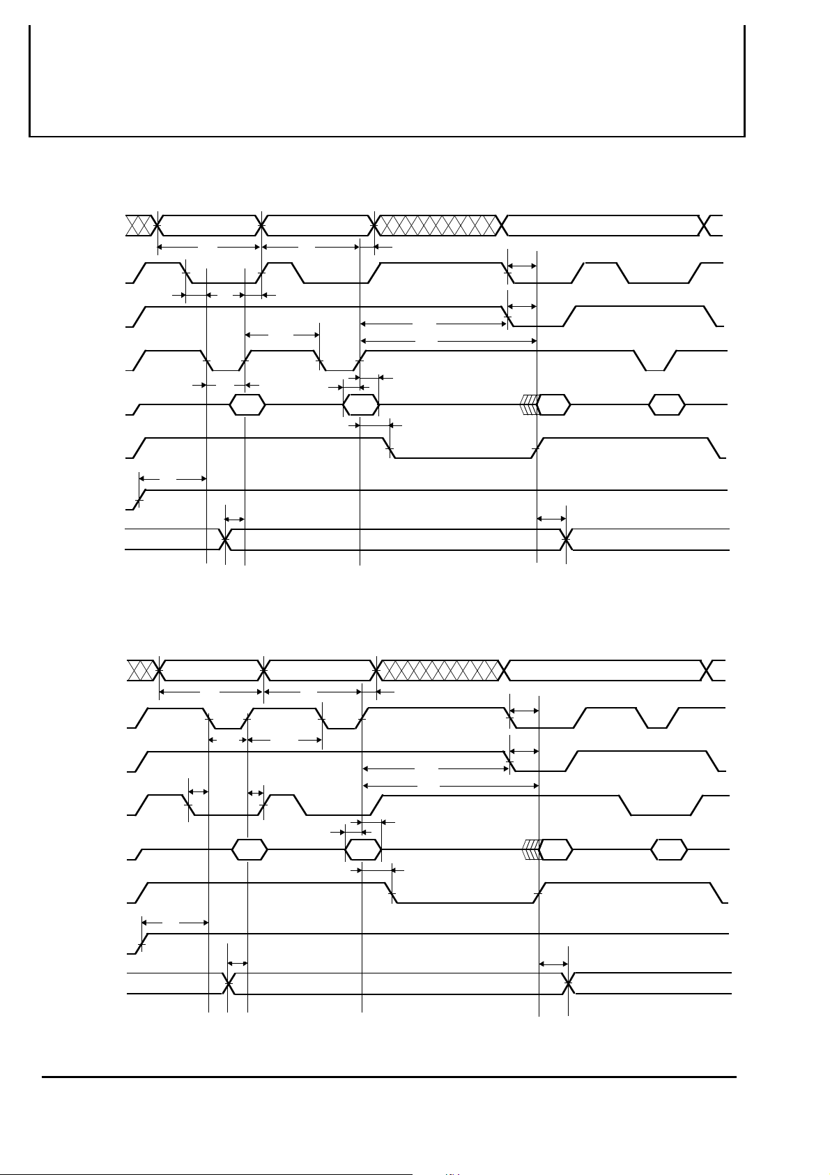
AC WAVEFORMS FOR PAGE PROGRAM OPERATION (F-WE# control)
The other bank
tOEH
address
VALID
VALID
tAH
ta(CE)
tDH
ta(OE)
DOUT
ADDRESS VALID
01H~7EH
tGHWL
DIN
F-A19~F-A17,
A16~A7
A6 ~A0
F-CE#
F-OE#
F-WE#
DATA
F-RY/BY#
F-RP#
F-WP#
VIH
BANK ADDRESS
VIL
VIH
VIL
VIH
VIL
tCS tCH
VIH
VIL
VIH
VIL
VIH
VIL
VOH
VOL
tPS
VIH
VIL
VIH
VIL
VALID
tWC
tWP
41H DIN
VALID
00H
tAS
tWPH
tDS
tBLS
7FH
DIN
PROGRAM
tOEH
tDAP
tWHRL
READ STATUS
REGISTER
BANK ADDRESS VALID
ARRAY COMMAND
ta(CE)
ta(OE)
SRD
tBLH
WRITE READ
FFH
AC WAVEFORMS FOR PAGE PROGRAM OPERATION (F-CE# control)
The other bank
F-A19~F-A17,
A16~A7
A6 ~A0
F-CE#
F-OE#
F-WE#
DATA
F-RY/BY#
F-RP#
F-WP#
VIH
VIL
VIH
VIL
VIH
VIL
VIH
VIL
VIH
VIL
VIH
VIL
VOH
VOL
VIH
VIL
VIH
VIL
BANK ADDRESS
VALID
tWC
tCEP
tWS tWH
tPS
tAS
tCEPH
tDS
41H DIN
tBLS
address
VALIDVALID
VALID
tAH
ta(CE)
ta(OE)
tOEH tGHEL
tDH
DOUT
ADDRESS VALID
01H~7EH00H
DIN SRDDIN
7FH
PROGRAM
tOEH
tDAP
tEHRL
READ STATUS
REGISTER
BANK ADDRESS VALID
ARRAY COMMAND
ta(CE)
ta(OE)
tBLH
WRITE READ
FFH
14
Nov 1999 , Rev.2.3

MITSUBISHI LSIs
M6MGB/T166S2BWG
16,777,216-BIT (1,048,576 -WORD BY 16-BIT ) CMOS
3.3V-ONLY FLASH MEMORY &
2,097,152-BIT (131,072-WORD BY 16-BIT) CMOS SRAM
Stacked-CSP (Chip Scale Package)
AC WAVEFORMS FOR WORD PROGRAM OPERATION (F-WE# control) (to only BANK(I))
ADDRESSES
F-CE#
F-OE#
F-WE#
DATA
F-RY/BY#
F-RP#
F-WP#
VIH
VIL
VIH
VIL
VIH
VIL
VIH
VIL
VIH
V
VIH
V
VIH
VIL
VIH
VIL
WRITE READ
ARRAY COMMAND
ta(CE)
ta(OE)
BANK ADDRESS
tCS
VALID
ADDRESS
VALID
tAStWC
tCH
tWP
tAH
PROGRAM
tOEH
READ STATUS
REGISTER
BANK(I) ADDRESS VALID
tWPH
tDS
IL
40H DIN
SRD FFH
tDH
IL
tPS
tWHRL
tDAP
tBLS
tBLH
AC WAVEFORMS FOR WORD PROGRAM OPERATION (F-CE# control) (to only BANK(I))
READ STATUS
REGISTER
BANK(I) ADDRESS VALID
ta(CE)
ta(OE)
SRD FFH
ADDRESSES
F-CE#
F-OE#
F-WE#
DATA
F-RY/BY#
F-RP#
F-WP#
VIH
VIL
VIH
VIL
VIH
VIL
VIH
VIL
VIH
V
VIH
VIL
VIH
VIL
VIH
VIL
PROGRAM
tOEH
BANK ADDRESS
tWS
VALID
ADDRESS
VALID
tAStWC
tCEP
tWH
tAH
tDS
IL
40H DIN
tDH
tEHRL
tPS
tDAP
tBLS
WRITE READ
ARRAY COMMAND
tBLH
15
Nov 1999 , Rev.2.3
AC WAVEFORMS FOR ERASE OPERATIONS (F-WE# control)
ADDRESSES
F-CE#
F-OE#
F-WE#
DATA
F-RY/BY#
F-RP#
F-WP#
VIH
VIL
VIH
VIL
VIH
VIL
VIH
VIL
VIH
VIL
VOH
VOL
VIH
VIL
VIH
VIL
BANK ADDRESS
VALID
ADDRESS VALID
tWC
tCS tCH
tWPH
tWP
20H D0H
tPS
tBLS
tAS
tDS
MITSUBISHI LSIs
M6MGB/T166S2BWG
16,777,216-BIT (1,048,576 -WORD BY 16-BIT ) CMOS
3.3V-ONLY FLASH MEMORY &
2,097,152-BIT (131,072-WORD BY 16-BIT) CMOS SRAM
Stacked-CSP (Chip Scale Package)
tAH
tDH
tOEH
tDAE
tWHRL
ERASE
READ STATUS
REGISTER
BANK ADDRESS VALID
ta(CE)
ta(OE)
tBLH
WRITE READ
ARRAY COMMAND
FFHSRD
AC WAVEFORMS FOR ERASE OPERATIONS (F-CE# control)
ADDRESSES
F-CE#
F-OE#
F-WE#
DATA
F-RY/BY#
F-RP#
F-WP#
VIH
VIL
VIH
VIL
VIH
VIL
VIH
VIL
VIH
VIL
VOH
VOL
VIH
VIL
VIH
VIL
BANK ADDRESS
VALID
tWC
tWS
tPS
ADDRESS VALID
tAS
tCEP
tCEPH
tWH
tDS
20H D0H
tBLS
tAH
tDH
tOEH
tDAE
tEHRL
ERASE
READ STATUS
REGISTER
BANK ADDRESS VALID
ta(CE)
ta(OE)
tBLH
WRITE READ
ARRAY COMMAND
FFHSRD
16
Nov 1999 , Rev.2.3

M6MGB/T166S2BWG
16,777,216-BIT (1,048,576 -WORD BY 16-BIT ) CMOS
3.3V-ONLY FLASH MEMORY &
2,097,152-BIT (131,072-WORD BY 16-BIT) CMOS SRAM
Stacked-CSP (Chip Scale Package)
AC WAVEFORMS FOR PAGE PROGRAM OPERATION WITH BGO (F-WE# control)
Change Bank Address
PROGRAM DATA TO ONE BANK
F-A19~F-A17,
A16~A7
A6 ~A0
F-CE#
F-OE#
F-WE#
DATA
F-RY/BY#
VIH
VIL
VIH
VIL
VIH
VIL
VIH
VIL
VIH
VIL
VIH
VIL
VIH
VIL
BANK ADDRESS
tCS
VALID
tWC tAS
tCH
tWP
tWPH
41H DIN
00H
01H~7EH
tAH
tDS
tDH
ADDRESS VALID
~
~
~
~
~
~
~
~
7FH
tOEH
~
~
DIN DIN SRD
~
~
tWHRL
MITSUBISHI LSIs
ARRAY READ FROM THE OTHER BANK
WITH BGO
VALID VALID
VALID VALID
ta(CE)
ta(OE)
DOUT
DOUT
AC WAVEFORMS FOR PAGE PROGRAM OPERATION WITH BGO (F-CE# control)
Change Bank Address
PROGRAM DATA TO ONE BANK
F-A19~F-A17,
A16~A7
A6 ~A0
F-CE#
F-OE#
F-WE#
DATA
F-RY/BY#
VIH
VIL
VIH
VIL
VIH
VIL
VIH
VIL
VIH
VIL
VIH
VIL
VIH
VIL
BANK ADDRESS
tCEP
tWS
VALID
tWC
tCEPH
41H DIN
tAS
tCH
00H
ADDRESS VALID
~
~
01H~7EH
~
~
7FH
tAH
~
~
~
~
~
~
tDS
DIN DIN SRD
~
~
tDH
tOEH
tEHRL
ARRAY READ FROM THE OTHER BANK
WITH BGO
VALID VALID
VALID VALID
ta(CE)
ta(OE)
DOUT
DOUT
17
Nov 1999 , Rev.2.3

M6MGB/T166S2BWG
16,777,216-BIT (1,048,576 -WORD BY 16-BIT ) CMOS
3.3V-ONLY FLASH MEMORY &
2,097,152-BIT (131,072-WORD BY 16-BIT) CMOS SRAM
Stacked-CSP (Chip Scale Package)
AC WAVEFORMS FOR WORD PROGRAM OPERATION WITH BGO (F-WE# control)
Change Bank Address
F-A19~F-A17,
A16~A7
A6 ~A0
F-CE#
F-OE#
F-WE#
DATA
F-RY/BY#
VIH
VIL
VIH
VIL
VIH
VIL
VIH
VIL
VIH
VIL
VIH
VIL
VIH
VIL
BANK ADDRESS
tCS
PROGRAM DATA TO
BANK(I)
VALID
VALID
tWC tAS
ADDRESS VALID
tAH
tCH
tWP
tOEH
tWPH
tDS
40H DIN SRD
tDH
tWHRL
READ STATUS
REGISTER
MITSUBISHI LSIs
ARRAY READ FROM BANK(II) WITH BGO
VALID VALID
VALID VALID
ta(CE)
ta(OE)
DOUT
DOUT
AC WAVEFORMS FOR WORD PROGRAM OPERATION WITH BGO (F-CE# control)
Change Bank Address
F-A19~F-A17,
A16~A7
A6 ~A0
F-CE#
F-OE#
F-WE#
DATA
F-RY/BY#
VIH
VIL
VIH
VIL
VIH
VIL
VIH
VIL
VIH
VIL
VIH
VIL
VIH
VIL
BANK ADDRESS
tCEP
tWS
READ STATUS
REGISTER
ADDRESS VALID
VALID
tWC
PROGRAM DATA TO
BANK(I)
VALID
tAS
tCEPH
tOEH
tCH
tDS
40H DIN SRD DOUT
tDH
tEHRL
ARRAY READ FROM BANK(II) WITH BGO
VALID VALID
VALID VALID
ta(CE)
ta(OE)
DOUT
18
Nov 1999 , Rev.2.3

M6MGB/T166S2BWG
16,777,216-BIT (1,048,576 -WORD BY 16-BIT ) CMOS
3.3V-ONLY FLASH MEMORY &
2,097,152-BIT (131,072-WORD BY 16-BIT) CMOS SRAM
Stacked-CSP (Chip Scale Package)
AC WAVEFORMS FOR BLOCK ERASE OPERATION WITH BGO (F-WE# control)
Change Bank Address
READ STATUS
ADDRESS VALID
tOEH
tDS
tDH
tWHRL
REGISTER
tAH
ADDRESSES
F-CE#
F-OE#
F-WE#
DATA
F-RY/BY#
VIH
VIL
VIH
VIL
VIH
VIL
VIH
VIL
VIH
VIL
VIH
VIL
BANK ADDRESS
tCS
BLOCK ERASE IN
ONE BANK
VALID
tWC tAS
tCH
tWP
tWPH
20H D0H SRD
MITSUBISHI LSIs
ARRAY READ FROM THE OTHER
BANK WITH BGO
VALID VALID
ta(CE)
ta(OE)
DOUT
DOUT
AC WAVEFORMS FOR BLOCK ERASE OPERATION WITH BGO (F-CE# control)
Change Bank Address
ADDRESSES
F-CE#
F-OE#
F-WE#
DATA
F-RY/BY#
VIH
VIL
VIH
VIL
VIH
VIL
VIH
VIL
VIH
VIL
VIH
VIL
BANK ADDRESS
tCEP
tWS
BLOCK ERASE IN
ONE BANK
VALID
tWC
tAS
tCEPH
tCH
20H D0H SRD DOUT
READ STATUS
REGISTER
ADDRESS VALID
tOEH
tDS
tDH
tAH
tEHRL
READ DATA FROM THE OTHER BANK
WITH BGO
VALID VALID
ta(CE)
ta(OE)
DOUT
19
Nov 1999 , Rev.2.3

16,777,216-BIT (1,048,576 -WORD BY 16-BIT ) CMOS
2,097,152-BIT (131,072-WORD BY 16-BIT) CMOS SRAM
AC WAVEFORMS FOR SUSPEND OPERATION (F-WE# control)
ADDRESSES
F-CE#
F-OE#
F-WE#
DATA
VIH
VIL
VIH
VIL
VIH
VIL
VIH
VIL
VIH
VIL
BANK ADDRESS VALID
tAS
tCS
tWP
B0H
tAH
tCH
tOEH
Program Suspend Latency
MITSUBISHI LSIs
M6MGB/T166S2BWG
3.3V-ONLY FLASH MEMORY &
Stacked-CSP (Chip Scale Package)
READ STATUS
REGISTER
BANK ADDRESS VALID
ta(CE)
ta(OE)
S.R.6,7=1
VALID SRD
F-RY/BY#
F-RP#
F-WP#
VOH
VOL
VIH
VIL
VIH
VIL
tBLS
AC WAVEFORMS FOR SUSPEND OPERATION (F-CE# control)
ADDRESSES
F-CE#
F-OE#
F-WE#
DATA
VIH
VIL
VIH
VIL
VIH
VIL
VIH
VIL
VIH
VIL
BANK ADDRESS VALID
tAS
tCEP
tWS
B0H
tAH
tOEH
Program Suspend Latency
tWH
tBLH
READ STATUS
REGISTER
BANK ADDRESS VALID
ta(CE)
ta(OE)
S.R.6,7=1
VALID SRD
20
F-RY/BY#
F-RP#
F-WP#
VOH
VOL
VIH
VIL
VIH
VIL
tBLS
tBLH
Nov 1999 , Rev.2.3

MITSUBISHI LSIs
M6MGB/T166S2BWG
16,777,216-BIT (1,048,576 -WORD BY 16-BIT ) CMOS
3.3V-ONLY FLASH MEMORY &
2,097,152-BIT (131,072-WORD BY 16-BIT) CMOS SRAM
Stacked-CSP (Chip Scale Package)
FULL STATUS CHECK PROCEDURE
STATUS REGISTER
READ
SR.4 =1
and
SR.5 =1
?
SR.5 = 0 ?
SR.4 = 0 ?
SR.3 = 0 ?
SUCCESSFUL
(BLOCK ERASE, PROGRAM)
YES
NO
NO
YES
NO
YES
NO
YES
WORD PROGRAM FLOW CHART
COMMAND SEQUENCE ERROR
BLOCK ERASE ERROR
PROGRAM ERROR
(PAGE, LOCK BIT)
PROGRAM ERROR
(BLOCK)
LOCK BIT PROGRAM FLOW CHART
START
WRITE 77H
WRITE D0H
BLOCK ADDRESS
SR.7 = 1 ?
SR.4 = 0 ?
LOCK BIT PROGRAM
SUCCESSFUL
NO
YES
NO
YES
PAGE PROGRAM FLOW CHART
LOCK BIT PROGRAM
FAILED
START
WRITE 40H
WRITE
ADDRESS , DATA
STATUS REGISTER
READ
SR.7 = 1 ?
FULL STATUS CHECK
IF DESIRED
WORD PROGRAM
COMPLETED
NO
YES
* Word program is admitted to only BANK(I).
WRITE B0H ?
YES
SUSPEND LOOP
WRITE D0H
YES
NO
START
WRITE 41H
n = 0
WRITE
ADDRESS n, DATA n
n = FFH ?
or
n = 7FH ?
YES
STATUS REGISTER
READ
SR.7 = 1 ?
YES
NO
NO
WRITE B0H ?
YES
n = n+1
NO
21
FULL STATUS CHECK
IF DESIRED
PAGE PROGRAM
COMPLETED
SUSPEND LOOP
WRITE D0H
YES
Nov 1999 , Rev.2.3

MITSUBISHI LSIs
M6MGB/T166S2BWG
16,777,216-BIT (1,048,576 -WORD BY 16-BIT ) CMOS
3.3V-ONLY FLASH MEMORY &
2,097,152-BIT (131,072-WORD BY 16-BIT) CMOS SRAM
Stacked-CSP (Chip Scale Package)
CLEAR PAGE BUFFER
START
WRITE 55H
WRITE D0H
PAGE BUFFER CLEAR
COMPLETED
SINGLE DATA LOAD TO PAGE BUFFER
START
WRITE 74H
WRITE
ADDRESS , DATA
DONE
LOADING?
NO
SUSPEND / RESUME FLOW CHART
START
WRITE B0H
STATUS REGISTER
READ
SR.7 = 1?
YES
SR.6 =1?
YES
WRITE FFH
READ ARRAY DATA
DONE
READING ?
YES
WRITE D0H
NO
NO
NO
SUSPEND
PROGRAM / ERASE
RESUME
COMPLETED
YES
SINGLE DATA LOAD
TO PAGE BUFFER
COMPLETED
PAGE BUFFER TO FLASH
START
WRITE 0EH
WRITE D0H
PAGE ADDRESS
STATUS REGISTER
READ
SR.7 = 1 ?
FULL STATUS CHECK
IF DESIRED
PAGE BUFFER TO FLASH
COMPLETED
NO
WRITE B0H ?
YES
SUSPEND LOOP
WRITE D0H
YES
NO
OPERATION
RESUMED
* The bank address is required when writing this command. Also, there is
no need to suspend the erase or program operation when reading data
from the other bank. Please use BGO function.
BLOCK ERASE FLOW CHART
START
WRITE 20H
WRITE D0H
BLOCK ADDRESS
STATUS REGISTER
READ
SR.7 = 1 ?
YES
FULL STATUS CHECK
IF DESIRED
BLOCK ERASE
COMPLETED
NO
WRITE B0H ?
SUSPEND LOOP
WRITE D0H
NO
YES
YES
22
Nov 1999 , Rev.2.3
23
OPERATION STATUS and EFFECTIVE COMMAND
Read/Standby State
Setup State
Clear
Page Buffer
Setup
Clear
Status Register
55H
Single Data Load
to Page Buffer
Setup
74H
Ready
50H
D0H
Page Buffer to Flash
WD
Setup
OTHER
Internal State
90H
Read
Device Identifier
90H
FFH
0EH
Page Program
Setup
D0H
Status Register
Read
Status Register
70H
90H
70H
FFH
Read Array
41H 77H
70H
71H
71H
71H
FFH
40H
Word Program
Setup
WDi
i=0-127
WD
D0H
Program &
Verify
Read
D0H
Read
Lock Status
Lock Bit Program
Setup
OTHER
B0H
B0H D0H
Change Bank
Address
20H
Block Erase
Setup
Erase &
Verify
Read
Status Register
(From The Other Bank)
A7H
Erase All Unlocked
OTHER OTHER
D0HD0H
Read Array
Blocks Setup
16,777,216-BIT (1,048,576 -WORD BY 16-BIT ) CMOS
2,097,152-BIT (131,072-WORD BY 16-BIT) CMOS SRAM
3.3V-ONLY FLASH MEMORY &
Stacked-CSP (Chip Scale Package)
M6MGB/T166S2BWG
Nov 1999 , Rev.2.3
Change Bank
Address
Read State with BGO
Read Array
(From The Other Bank)
Change Bank
Address
Suspend State
Read
Status Register
70H
FFH
Read Array
70H
MITSUBISHI LSIs

2. SRAM
MITSUBISHI LSIs
M6MGB/T166S2BWG
16,777,216-BIT (1,048,576 -WORD BY 16-BIT ) CMOS
3.3V-ONLY FLASH MEMORY &
2,097,152-BIT (131,072-WORD BY 16-BIT) CMOS SRAM
Stacked-CSP (Chip Scale Package)
The SRAM of M6MGB/T166S2BWG is organized as
131,072-word by 16-bit. These devices operate on a single
+2.7~3.6V powersupply, and are directly TTL compatible to both
input and output. Its fully static circuit needs no clocks and no
refresh, and makes it useful.
The operation mode are determined by a combination of the
device control inputs , S-LB#,S-UB#,S-CE1#,S-CE2, S-WE#
and S-OE#. Each mode is summarized in the function table.
A write operation is executed whenever the low level S-WE#
overlaps with the low level S-LB# and/or S-UB# and the low
level S-CE1#the high level S-CE2. The address A0~A16 must
be set up before the write cycle and must be stable during the
entire cycle.
A read operation is executed by setting S-WE# at a high level
and S-OE# at a low level while S-LB# and/or S-UB# and
S-CE1# and S-CE2 are in an active state(S-CE1#=L,S-CE2=H).
When setting S-LB# at the high level and other pins are in
an active stage, upper-byte are in selectable mode in which
both reading and writing are enabled, and lower-byte are in
non-selectable mode. And when setting S-UB# at a high
level and other pins are in an active stage, lower-byte are in
a selectable mode and upper-byte are in a non-selectable
mode.
When setting S-LB# and S-UB# at a high level or S-CE1#
at high level or S-CE2 at a low level, the chips are in a nonselectable mode in which both reading and writing are
disabled. In this mode, the output stage is in a highimpedance state, allowing OR-tie with other chips and
memory expansion by S-LB#,S-UB# and S-CE1#,S-CE2.
The power supply current is reduced as low as
0.3mA(25°C,typical), and the memory data can be held at
+2V powersupply, enabling battery back-up operation during
power failure or power-down operation in the non-selected
mode.
FUNCTION TABLE
X
Non selection
Non selection
X
Non selection
X
Non selection
X
X
L
H
X
L
H
X
L
H
Mode
Write
Read Dout
Write
Read
Write
Read
DQ0~7
High-Z
High-Z
High-Z
High-Z
Din
High-Z
High-Z
High-Z
High-Z
Din
Dout
High-Z
DQ8~15
High-Z
High-Z
High-Z
High-Z
High-Z
High-Z
High-Z
Din
Dout
High-Z
Din
Dout
High-Z
S-LB#S-CE2S-CE1#
H
L
H
X
L
L
L
L
L
L
L
L
L
L
L
H
X
H
H
H
H
H
H
H
H
H
S-UB#
X
X
X
H
L
L
L
H
H
H
L
L
L
S-WE#
X
X
X
H
H
H
H
L
L
L
L
L
L
S-OE#
X
X
X
X
L
H
H
L
H
H
L
H
H
Icc
Standby
Standby
Standby
Standby
Active
Active
Active
Active
Active
Active
Active
Active
Active
24
Nov 1999 , Rev.2.3

ABSOLUTE MAXIMUM RATINGS
MITSUBISHI LSIs
M6MGB/T166S2BWG
16,777,216-BIT (1,048,576 -WORD BY 16-BIT ) CMOS
3.3V-ONLY FLASH MEMORY &
2,097,152-BIT (131,072-WORD BY 16-BIT) CMOS SRAM
Stacked-CSP (Chip Scale Package)
Symbol Parameter Units
S-V
V
VO
Pd
Ta
Tstg
Supply voltage
cc
Input voltage
I
Output voltage
Power dissipation
Operating
temperature
Storage temperature
DC ELECTRICAL CHARACTERISTICS
Symbol
VIH
VIL
VOH1
V
OH2
V
OL
I
I
IO
1
Icc
Icc2
Icc3
Parameter
High-level input voltage
Low-level input voltage
High-level output voltage 1
High-level output voltage 2
Low-level output voltage
Input leakage current
Output leakage current
Active supply current
( AC,MOS level )
Active supply current
( AC,TTL level )
Stand by supply current
( AC,MOS level )
Conditions Units
IOH= -0.5mA
IOH= -0.05mA
IOL=2mA
VI =0 ~ S-Vcc
S-LB# and S-UB#=VIH or S-CE1#=VIH or S-CE2=VIH
or S-OE#=VIH, VI/O=0 ~ S-Vcc
S-LB# and S-UB# 0.2V,S-CE1# 0.2V,
>
S-CE2 (S-Vcc)-0.2V other inputs 0.2V or
=
(S-Vcc)-0.2V Output-open(duty 100%)
S-LB# and S-UB#=VIL,S-CE1#=VIL,
S-CE2=VIH other inputs=VIH or VIL
Output-open(duty 100%)
S-CE2 0.2V
Other inputs=0~S-Vcc
<
=
<
=
Conditions
With respect to GND
With respect to GND
With respect to GND
Ta=25°C
I-version
<
=
<
>
=
=
+70 ~ +85 °C
+40 ~ +70 °C
+25 ~ +40 °C
Ratings
-0.5* ~ +4.6
-0.5
* ~ S-Vcc + 0.5
V
0 ~ S-Vcc
700
- 40 ~ +85
- 65 ~ +150
* -3.0V in case of AC (Pulse width 30ns)
( S-Vcc=2.7 ~ 3.6V, unless otherwise noted)
Limits
Min
Typ
2.0
-0.3 *
mW
°C
°C
<
=
Max
(S-Vcc)+0.3V
0.6
2.4
(S-Vcc)-0.5V
0.4
+/- 1
+/- 1
f= 10MHz
f= 1MHz
f= 10MHz
f= 1MHz
-
-
5
-
-
-
-
-
-
-
15
6045
15
6045
155
30
10
V
mA
mA
mA
Stand by supply current
Icc4
( AC,TTL level )
Note 1: Direction for current flowing into IC is indicated as positive (no mark)
Note 2: Typical value is for S-Vcc=3.0V and Ta=25°C
S-LB# and S-UB#=VIH or S-CE1#=VIH or S-CE2=VIL
Other inputs= 0 ~ S-Vcc
CAPACITANCE
Symbol
CI
CO
Note: The value of common pins to SRAM is the sum of Flash Memory and SRAM.
25
Parameter
Input capacitance
Output capacitance
Conditions
VI=GND, VI=25mVrms, f=1MHz
O=GND,VO=25mVrms, f=1MHz
V
- 40 ~ +25 °C
* -3.0V in case of AC (Pulse width 30ns)
(S-Vcc=2.7 ~ 3.6V, unless otherwise noted)
- 0.3 2
-
-
Limits
1.0
MaxTypMin
8
10
Nov 1999 , Rev.2.3
mA
<
=
Units
pF

MITSUBISHI LSIs
M6MGB/T166S2BWG
16,777,216-BIT (1,048,576 -WORD BY 16-BIT ) CMOS
3.3V-ONLY FLASH MEMORY &
2,097,152-BIT (131,072-WORD BY 16-BIT) CMOS SRAM
Stacked-CSP (Chip Scale Package)
AC ELECTRICAL CHARACTERISTICS
(S-Vcc=2.7 ~ 3.6V, unless otherwise noted)
(1) TEST CONDITIONS
Supply voltage
Input pulse
Input rise time and fall time
Reference level
Output loads
2.7V~3.6V
IH=2.2V, VIL=0.4V
V
5ns
V
OH=VOL=1.5V
Transition is measured 500mV from
steady state voltage.(for t
+
-
en,tdis)
Fig.1,CL=30pF
CL=5pF (for ten,tdis)
(2) READ CYCLE
Limits
Symbol
t
CR ns
ta(A)
ta(CE1)
Read cycle time
Address access time
Chip enable 1 access time
Parameter
ta(CE2)
ta(LB)
ta(UB)
ta(OE)
tdis(CE1)
tdis(CE2)
tdis(LB)
tdis(UB)
tdis(OE)
ten(CE1)
ten(CE2)
tdis(LB)
tdis(UB)
ten(OE)
tV(A)
Lower Byte control access time
Upper Byte control access time
Output enable access time
Output disable time after S-CE1# high
Output disable time after S-CE2 low
Output disable time after S-LB# high
Output disable time after S-UB# high
Output disable time after S-OE high
Output enable time after S-CE1# low
Output enable time after S-CE2 high
Output enable time after S-LB# low
Output enable time after S-UB# low
Output enable time after S-OE low
Data valid time after address
SRAM
85
10
10
10
10
5
10
MaxMin
85
85
85
85
45
30
30
30
30
30
1TTL
DQ
CL
Including scope and
jig capacitance
Fig.1 Output load
Units
ns
ns
nsChip enable 2 access time 85
ns
ns
ns
ns
ns
ns
ns
ns
ns
ns
ns
ns
ns
ns
(3) WRITE CYCLE
Symbol Parameter
tCW
tw(W)
tsu(A)
tsu(A-WH)
tsu(LB)
tsu(UB)
tsu(CE1)
tsu(CE2)
tsu(D)
th(D)
trec(W)
tdis(W)
tdis(OE)
ten(W)
ten(OE)
26
Write cycle time
Write pulse width
Address setup time
Address setup time with respect to S-WE#
Lower Byte control setup time
Upper Byte control setup time
Chip enable 1 setup time
Chip enable 2 setup time ns
Data setup time
Data hold time
Write recovery time
Output disable time from S-WE# low
Output disable time from S-OE# high
Output enable time from S-WE# high
Output enable time from S-OE# low
50
70
70
70
70
70
35
0
0
0
5
5
Limits
SRAM
MaxMin
30
30
Units
ns85
ns
ns
ns
ns
ns
ns
ns
ns
ns
ns
ns
ns
ns
Nov 1999 , Rev.2.3

(4)TIMING DIAGRAMS
Read cycle
A0~16
S-LB#,
S-UB#
S-CE1#
(Note3)
(Note3) (Note3)
ta(LB)
ta(CE1)
MITSUBISHI LSIs
M6MGB/T166S2BWG
16,777,216-BIT (1,048,576 -WORD BY 16-BIT ) CMOS
3.3V-ONLY FLASH MEMORY &
2,097,152-BIT (131,072-WORD BY 16-BIT) CMOS SRAM
Stacked-CSP (Chip Scale Package)
tCR
ta(A)
or
ta(UB)
tdis (LB) or tdis (UB)
tv
(A)
tdis (CE1)
(Note3)
S-CE2
S-OE#
S-WE# = "H" level
DQ0~15
Write cycle
0~16
A
S-LB#,
S-UB#
S-CE1#
ta(CE2)
(Note3) (Note3)
tdis (CE2)
ta (OE)
(Note3)
ten (OE)
tdis (OE)
ten (LB)
ten (UB)
ten (CE1)
VALID DATA
ten (CE2)
(S-WE# control mode)
tCW
tsu (LB) or tsu(UB)
(Note3) (Note3)
tsu (CE1)
(Note3)
S-CE2
S-OE#
S-WE#
DQ0~15
27
(Note3) (Note3)
tsu (CE2)
(Note3) (Note3)
tsu (A-WH)
tsu (A)
tw (W)
trec (W)
tdis (W)
ten(OE)
tdis(OE)
DATA IN
STABLE
ten (W)
th (D)tsu (D)
Nov 1999 , Rev.2.3

Write cycle (S-LB#,S-UB# control mode)
A0~16
MITSUBISHI LSIs
M6MGB/T166S2BWG
16,777,216-BIT (1,048,576 -WORD BY 16-BIT ) CMOS
3.3V-ONLY FLASH MEMORY &
2,097,152-BIT (131,072-WORD BY 16-BIT) CMOS SRAM
Stacked-CSP (Chip Scale Package)
tCW
tsu (A)
tsu (LB) or
tsu(UB)
trec (W)
S-LB#,
S-UB#
S-CE1#
(Note3)(Note3)
S-CE2
(Note3)(Note3)
(Note3)(Note3)
S-WE#
(Note5)
(Note4)
th (D)tsu (D)
DQ0~15
Note 3: Hatching indicates the state is "don't care".
Note 4: A Write occurs during S-CE1# low, S-CE2 high overlaps S-LB# and/or S-UB# low and S-WE# low.
Note 5: When the falling edge of S-WE# is simultaneously or prior to the falling edge of S-LB# and/or S-UB# or the falling edge of
S-CE1# or rising edge of S-CE2, the outputs are maintained in the high impedance state.
Note 6: Don't apply inverted phase signal externally when DQ pin is in output mode.
DATA IN
STABLE
28
Nov 1999 , Rev.2.3

Write cycle (S-CE1# control mode)
A0~16
S-LB#,
S-UB#
(Note3)
S-CE1#
tsu (A)
tsu (CE1)
MITSUBISHI LSIs
M6MGB/T166S2BWG
16,777,216-BIT (1,048,576 -WORD BY 16-BIT ) CMOS
3.3V-ONLY FLASH MEMORY &
2,097,152-BIT (131,072-WORD BY 16-BIT) CMOS SRAM
Stacked-CSP (Chip Scale Package)
tCW
trec (W)
(Note3)
S-CE2
(Note3)
(Note5)
S-WE#
(Note3)
DQ0~15
Write cycle (S-CE2 control mode)
A0~16
S-LB#,
S-UB#
(Note3)
tsu (A)
S-CE1#
(Note4)
th (D)tsu (D)
DATA IN
STABLE
tCW
tsu (CE2) trec (W)
(Note3)
(Note3)
(Note3)
S-CE2
S-WE#
DQ0~15
29
(Note3)
(Note3)
(Note5)
(Note4)
DATA IN
STABLE
(Note3)
th (D)tsu (D)
(Note3)
Nov 1999 , Rev.2.3
POWER DOWN CHARACTERISTICS
(1) ELECTRICAL CHARACTERISTICS
MITSUBISHI LSIs
M6MGB/T166S2BWG
16,777,216-BIT (1,048,576 -WORD BY 16-BIT ) CMOS
3.3V-ONLY FLASH MEMORY &
2,097,152-BIT (131,072-WORD BY 16-BIT) CMOS SRAM
Stacked-CSP (Chip Scale Package)
Symbol
S-Vcc (PD)
VI (S-BC)
VI (S-CE1#)
VI (S-CE2)
Icc (PD)
Parameter Test conditions
Power down supply voltage
Byte control input S-LB#,S-UB#
Chip enable input S-CE1#
Chip enable input S-CE2
Power down
supply current
(2) TIMING REQUIREMINTS
Symbol
tsu (PD)
trec (PD)
Parameter Test conditions
Power down set up time
Power down recovery time
(3) TIMING DIAGRAM
S-LB#,S-UB# control mode
S-Vcc
S-Vcc=3.0V
<
S-CE2 0.2V
=
other inputs=0~3V
-I
+70 ~ +85°C
+40 ~ +70°C
+25 ~ +40°C
- 40 ~ +25 °C
Limits
Min Typ Max
2.0
2.0
2.0
0.2
-
-
-
-
Min Typ Max
-
-
1
0.3
Typical value is for Ta=25°C
Limits
24
8
3
1
0
5
Units
V
V
V
V
mA
mA
mA
mA
Units
ns
ms
S-LB#,
S-UB#
S-CE1# control mode
S-Vcc
S-CE1#
S-CE2 control mode
S-Vcc
S-CE2
30
2.2V
2.2V
0.2V
tsu (PD)
tsu (PD)
tsu (PD)
2.7V2.7V
S-LB#,S-UB# (S-Vcc) - 0.2V
>
=
2.7V2.7V
S-CE1# (S-Vcc) - 0.2V
>
=
2.7V2.7V
S-CE2 0.2V
<
=
trec (PD)
2.2V
trec (PD)
2.2V
0.2V
trec (PD)
Nov 1999 , Rev.2.3
 Loading...