

MITSUBISHI 〈DIGITAL ASSP〉
MITSUBISHI 〈DIGITAL ASSP〉
DESCRIPTION
The M66516 is a semiconductor laser-diode driver/controller.
Its functions are the driving and laser power control of a specific type (Mitsubishi’s R type laser) of semiconductor laser
diode, in which the cathode of a semiconductor laser diode is
connected in stem structure to the anode of a monitoring
photodiode.
The IC has a laser drive current output pin of source type and
is capable of driving a laser diode on a maximum bias current
of 30mA and a maximum switching current of 120 mA, which
is switched at a rate of 20Mbits/sec.
Since the M66516 has a built in sample-hold circuit, it is pos-
∗
sible to realize an internal APC
system that requires no external device for laser power control.
∗: Automatic Power Control
FEATURES
• Built-in sample-hold circuit for APC function
• High speed switching (20Mbps)
• Large drive current (150mA max.)
• Capable of setting bias current (30mA max.)
• 5V single power supply
M66516FP
LASER-DIODE DRIVER/CONTROLLER
LASER-DIODE DRIVER/CONTROLLER
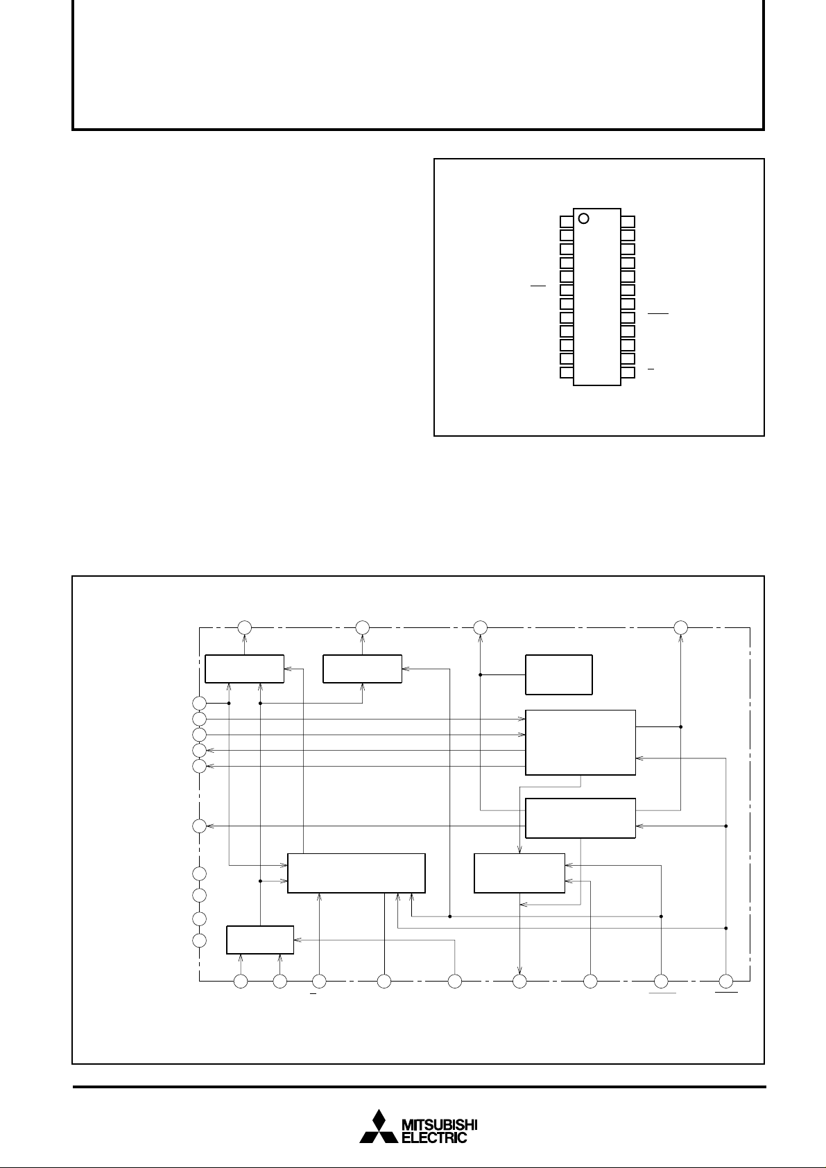
PIN CONFIGURATION (TOP VIEW)
SWITCHING CURRENT
SETTING INPUT 1
OUTPUT TO SWITCHING
CURRENT SETTING LOAD
SWITCHING CURRENT
SETTING INPUT 2
OUTPUT TO SWITCHING
CURRENT SETTING LOAD
LASER CURRENT
ENABLE INPUT
OUTPUT TO BIAS
CURRENT SETTING LOAD
MONITORING LOAD
MONITORING ANALOG
COMPARATOR OUTPUT
INPUTS
OUTPUT
MONITORING
1
VCC1
2
→
VL1
3
1RC
←
1
2
VL2
2RC
ENB
3RC
GND1
1RM
2RM
MO
CO
4
→
5
←
6
→
7
←
8
9
→
10
→
11
←
12
←
Outline 24P2N-B
24
23
22
21
M66516FP
20
19
18
17
16
15
14
13
M66516FP
OUTPUT TO LASER
RO
→
CURRENT LOAD
LASER CURRENT
LD
→
OUTPUT
NC
MONITORING DIODE
PD
←
INPUT
GND2
REFERENCE VOLTAGE
Vref
→
OUTPUT
REFERENCE VOLTAGE
Vr
←
INPUT
SWITCHING DATA
DATA
←
INPUT
DUTY CONTROL
CD
INPUT
VCC2
CONNECTION PIN FOR
CSH
SAMPLE-HOLD CAPACITOR
SAMPLE-HOLD
S/H
←
CONTROL INPUT
NC: No Connection
APPLICATION
Semiconductor laser-diode applied equipment
BLOCK DIAGRAM
V
SWITCHING CURRENT
SETTING INPUTS
V
1RC
2RC
3RC
V
GND
MONITORING
COMPARATOR OUTPUT
CO
COMPARATOR
V
r
18
2
L1
4
L2
3
5
7
1
CC
15
8
DIFFERENTIAL
20
AMP
ANALOG OUTPUT
MONITORING
MO
1112
LINEAR AMP
SAMPLE-HOLD
CIRCUIT
REFERENCE
VOLTAGE OUTPUT
V
ref
19
CURRENT
SWITCHING
CIRCUIT
RO
24
REFERENCE
VOLTAGE
SOURCE
SWITCHING
CURRENT
SOURCE
BIAS CURRENT
SOURCE
10
9
2RM PD LD
1RM
MONITORING
LOAD INPTUT
13
S/H
SAMPLE-HOLD
CONTROL INPUT
14
SH
C
CONNECTION
PIN FOR
DIODE INTPUT
MONITORING
SAMPLE-HOLD
CAPACITOR
21 23
OUTPUT TO
LASER
CURRENT LOAD
16
D
C
DUTY CONTROL
INPUT
17
DATA
SWITCHING
DATA INPUT
6
ENB
LASER CURRENT
ENABLE INPUT
1
PIN DESCRIPTIONS
Pin
LD
PD
VL1
1RC
VL2
2RC
3RC
DA T A
1RM, 2RM
MO
CO
ENB
RO
CD
S/H
CSH
Vref
Vr
VCC1
VCC2
GND1
GND2
Laser current output
Monitoring diode input
Switching current setting
input 1
Output to switching
current setting load 1
Switching current setting
input 2
Output to switching
current setting load 2
Output to bias current
setting load
Switching data input
Monitoring load input
Monitoring analog
output
Monitoring comparator
output
Laser current enable
input
Laser current load
output
Duty control input
Sample-hold control
input
Connection pin for
sample-hold capacitor
Reference voltage
output
Reference voltage input
Name
MITSUBISHI 〈DIGITAL ASSP〉
M66516FP
LASER-DIODE DRIVER/CONTROLLER
Description
Connect to anode on semiconductor laser diode.
Connect to cathode on monitoring photodiode.
Voltage input to set output current (IL1) of current source 1.
Connect load resistor between this pin and GND for IL1 setting.
Voltage input to set output current (IL2) of current source 2.
Connect a load resistor between this pin and GND for IL2 setting.
Connect a load resistor between this pin and GND for setting IB (bias current). Leave this
pin open if IB is not used.
If this pin is “L,” a current of IL1 + IL2 + IB flows through laser diode; if “H,” current IB flows.
Connect a load resistor between pins 1RM and 2RM for conversion of current generated by
monitoring photodiode into changes in voltage.
If DATA = “L” the potential difference generated on monitoring load resistor from photodiode
monitoring current is output as a voltage referenced to GND. If DATA = “H” the output at this
pin is fixed at “H” saturation level.
The potential difference generated on monitoring load resistor from photodiode monitoring
current is compared with the voltage on pin Vr. The result of the comparison is output in
TTL level.
This pin acts as comparator output pin only when S/H = “H” and DATA = “L.” In other states,
this output pin is fixed to “H.”
If this pin is “H,” all current supply circuits are turned off.
Connect a laser current load resistor between this pin and Vcc.
Connect a capacitor between this pin and GND for duty correction of light intensity
switching waveforms. If duty correction is not required, leave this pin open.
In internal APC mode, if this pin is “L,” sampling (APC) occurs, if “H,” holding (switching). In
external APC mode, connect this pin to Vcc.
Connect a capacitor for sample-hold function between this pin and GND.
Internal reference voltage (1.2V typ.) output pin of M66516
A reference voltage is applied to this pin to operate the comparator and the sample-hold
circuit. Connect this pin to the Vref pin if the internal reference voltage of the M66516 is
used.
Power supply for internal analog circuits. Connect to a positive power source (+5V).
Power supply for internal digital circuits. Connect to a positive power source (+5V).
GND for internal analog circuits.
GND for internal digital circuits.
2
MITSUBISHI 〈DIGITAL ASSP〉
M66516FP
LASER-DIODE DRIVER/CONTROLLER
OPERATION
1.Settings for Laser Drive Currents
The M66516 has built-in current sources for switching, IL1
and IL2, and a bias current source, IB. Each output current
can be controlled independently.
Approximate equations used for determining the current output from each of these current sources are as follows.
(1) IL1
IL1 is determined by the voltage on the VL1 pin and the resistor (RC 1) connected between the 1RC pin and GND.
The following equation is used for approximation.
IL1 [mA] = 12 ×
L2
(2) I
VL1 [V]
RC1 [kΩ]
IL2 is determined by the voltage on the VL2 pin and the resistor (RC 2) connected between the 2RC pin and GND.
The following equation is used for approximation.
IL2 [mA] = 12 ×
B
(3) I
VL2 [V]
RC2 [kΩ]
IB is determined by the internal reference voltage (Vref) and
the resistor (RC 3) connected between the 3RC pin and GND.
The following equation is used for approximation.
Buffer amp
LD
2RM
V
M
1RM
RM
+
−
Differential
amp
PD
V
r
−
+
+
−
Comparator
MO
CO
B [mA] = 10 ×
I
Vref [V]
RC3 [kΩ]
2.Laser Drive Current Switching Operation
If DA TA = “L,” laser drive current is I
I
B.
L1 + IL2 + IB; if DA TA = “H,”
3.Laser Power Monitoring Operation
At the MO and CO pins, the M66516 outputs data obtained
by the monitoring photodiode (PD) contained in laser, in the
sequence explained below.
(1) A current equal to the PD current generated from laser
light flows through the resistor (RM) inserted between 1RM
and 2RM. Thence a potential difference (V
M) occurring on
RM is converted by the internal differential amp. to a level
from GND.
M is output at the MO pin as an analog signal through a
(2) V
buffer amp. At the same time, the comparator compares V
with the voltage applied to the Vr pin, then the result of the
comparison is output at the CO pin in TTL level.
M < Vr , CO output = “L”; and if V M > Vr, CO output = “H.”
If V
As the condition of the above operation, both the MO and CO
output circuits should be in monitoring operation. See the
table below.
Monitor Function Table
Input Output
S/H
L
L
H
H
DATA
L
H
L
H
MO output
Analog output
“H” saturation
Analog output
“H” saturation
CO output
Fixed to “H”
Fixed to “H”
Comparator output
Fixed to “H”
M
A Schematic Diagram of Monitor Circuits
3
MITSUBISHI 〈DIGITAL ASSP〉
M66516FP
LASER-DIODE DRIVER/CONTROLLER
4. RO Pin
A load resistor for laser drive current is connected to the RO
pin, through which a current almost equal to laser drive current flows in(when DATA = “H”). A load resistor is connected
between the RO pin and Vcc to reduce power dissipated in
the IC.
Due to reasons related to the operation of circuits, the voltage
at this pin should be 3.5V or higher.
Consequently, the maximum resistance, RO
(max.), of load
resistor RO is:
(max.) (Ω) =
RO
Vcc (min.) – 3.5 [V]
LD (max.) [A]
I
where ILD (max.) is the maximum of laser drive current. If, for
Reference voltage V
RM resistor voltage
difference
Switching data
Sample-hold control
input
V
DATA
S/H
r
M
Control circuit
Comparator
+ logic
example, Vcc
(min.) = 4.75 V and ILD(max.) = 150 mA, RO (max.)
= 8.3 Ω. Accordingly, if the resistances of RC 1 to RC 3 is selected so as to gain a maximum laser drive current of 150mA,
RO should be 8.3Ω at the maximum.
5. ENB Input
If laser current is controlled by the DATA input, the current
source circuit is in operation even with zero laser current. If
ENB input = “H”, all current source circuits go off including the
bias current source.
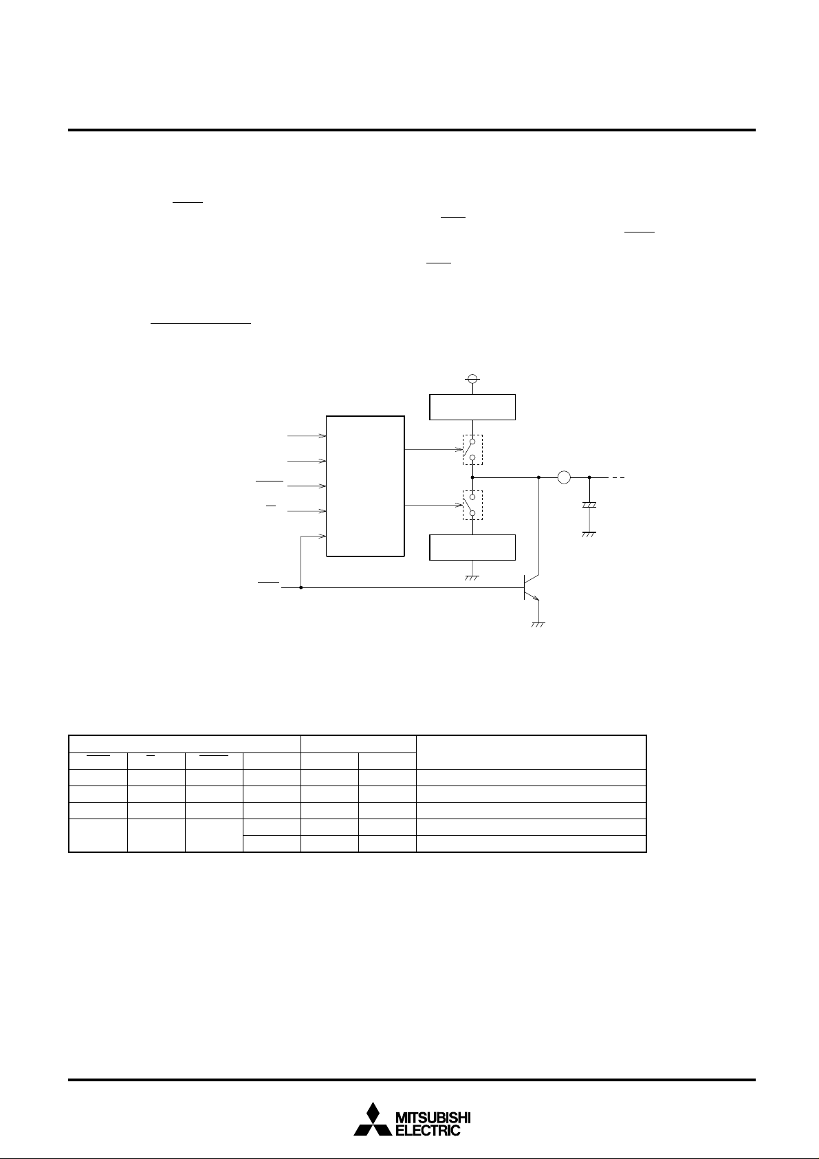
6. APC Operation
(1) Sample-hold circuit
The following are a conceptual diagram and function table of
the sample-hold circuit contained in the M66516.
Constant current
source for charging
SW1
Output
SW2
Constant current
source for discharging
SH
C
External capacitor
Function T able
ENB
H
L
L
L
×: Don’t care
S/H
×
H
L
L
Input
DATA
×
×
H
L
ENB
Conceptual Diagram: Sample-Hold Circuit
Switch condition
VM, Vr
×
×
×
VM < Vr
VM > Vr
SW1
OFF
OFF
OFF
ON
OFF
SW2
OFF
OFF
OFF
OFF
ON
Fixed to “L”
High impedance state (hold)
High impedance state (hold)
Constant current sourcing (sample)
Constant current sinking (sample)
Output
4
MITSUBISHI 〈DIGITAL ASSP〉
M66516FP
LASER-DIODE DRIVER/CONTROLLER
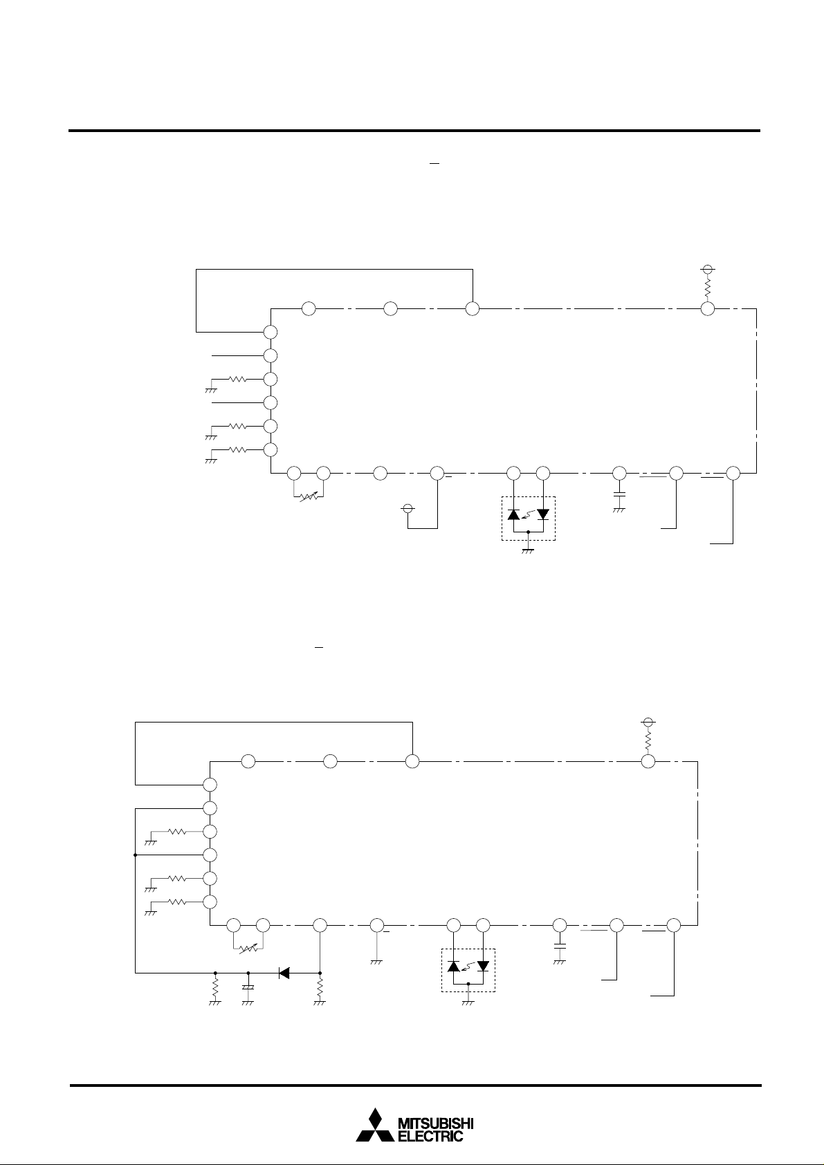
(2) External voltage-applied APC circuit
The following figure is an example of APC circuit configuration, in which voltages are applied from external sources to
L1 and VL2 input pins of the M66516. In this example, the
the V
14
MO
11
C
External control voltage 1
External control voltage 2
L1
V
1RC
VL2
2RC
3RC
Vr
18
2
3
4
5
7
1RM
CO
12
10
8
2RM
RM
S/H input pin is connected to Vcc and the C
SH pin is open.
The CO or MO output is used to monitor laser power for adjustment of external control voltage.
Vref
19
M66516FP
SH
13
S/H
PD
23
LD
1620
D
C
91pF
Data stream
17
DATA
Control signal
RO
24
ENB
6
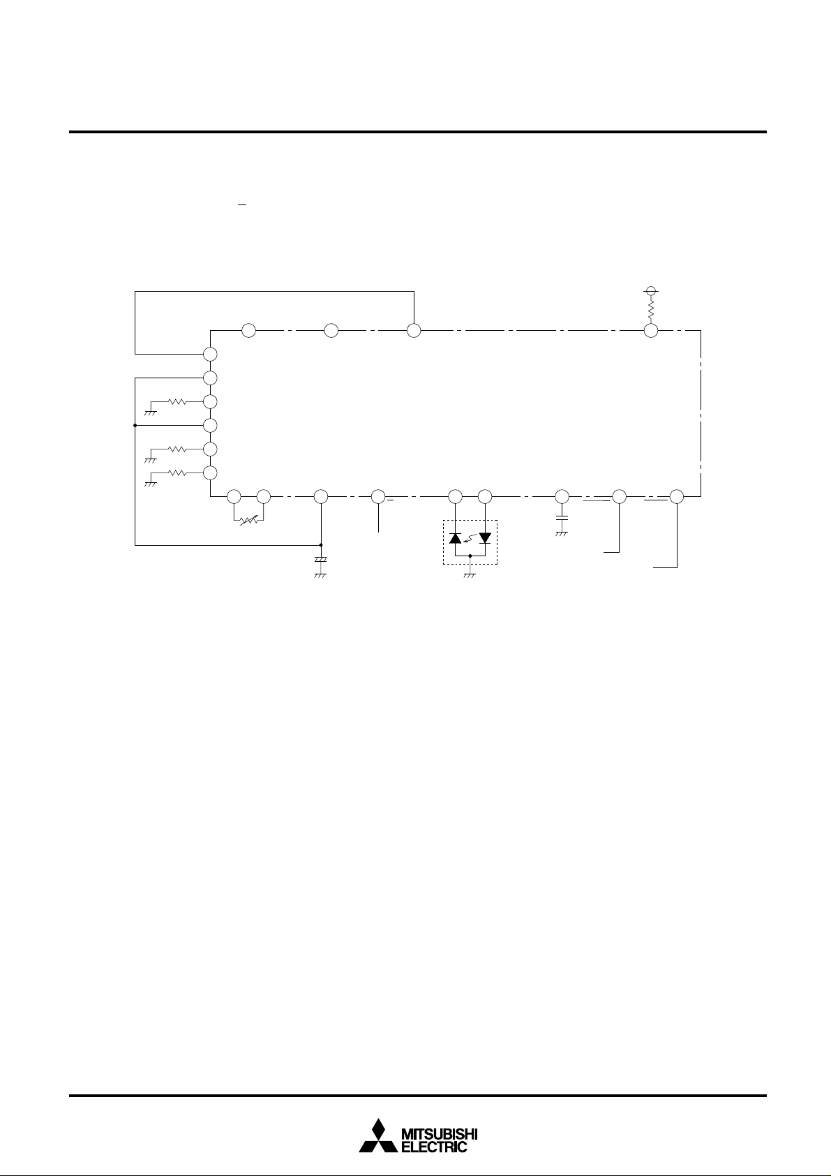
(3) Peak-holding internal APC circuit
The following figure is a configuration example of peak-holding internal APC circuit. In this example, the S/H input pin is
connected to GND.
L1
V
1RC
V
L2
2RC
3RC
CO
12
V
r
18
2
3
4
5
7
10
9
1RM
R1
2RM
RM
C1
14
MO
11
C
R2
SH
13
S/H
If laser power is lower than preset value, C1 is charged with
the current from the C
SH output pin through D1. The charge
stored in C1 is discharged through R1 thereafter.
V
ref
19
M66516FP
PD
21 23
LD
16
C
D
91pF
Data stream
DATA
Control signal
RO
24
17
6
ENB
C1, R1: Time constant components
R2: Pull–down resistor
(Used for establishing C
SH
line voltage in case that CSH is in high impedance condition.)
5
MITSUBISHI 〈DIGITAL ASSP〉
M66516FP
LASER-DIODE DRIVER/CONTROLLER
(4) Sample-hold type internal APC circuit
The following figure is a configuration example of samplehold type internal APC circuit. In this example, a sample-hold
control signal is applied to the S/H input pin.
In a sampling state, if laser power is lower than preset value,
14
MO
11
C
SH
C1
13
S/H
Control signal
V
r
18
2
V
L1
3
1RC
4
V
L2
5
2RC
7
3RC
1RM 2RM
CO
12
10
9
RM
C1 is charged by current from the C
SH output pin, while if it is
higher than preset value, C1 is discharged.
In a holding state, the CSH output is in high-impedance condition.
V
ref
19
M66516FP
PD
21 23
LD
16
D
C
91pF
Data stream
17
DATA
Control signal
RO
24
ENB
6
C1: Capacitor for sample–hold function
6
ABSOLUTE MAXIMUM RATINGS (Ta = –20 ~ 75°C, unless otherwise noted)
Parameter
VL1, VL2, Vr
DATE, ENB, S/H
CO
RO
“H” Output
“H” Output
Measured being mounted
Ta = 25°C (Note 1)
VCC
VI
VO
IL1
IL2
IB
Pd
Tstg
Symbol
Supply voltage
Input voltage
Output voltage
Output current 1
Output current 2
Bias current
Power dissipation
Storage temperature
SWITCHING CHARACTERISTICS (Ta = –20 ~ 75°C, unless otherwise noted)
Symbol
VCC
IL1
IL2
IB
Topr
Note 1: When Ta ≥ 25°C, derate by 7.1mW/°C
Supply voltage
Output current 1
Output current 2
Bias current
Operational ambient temperature
Parameter
Conditions
Conditions
MITSUBISHI 〈DIGITAL ASSP〉
M66516FP
LASER-DIODE DRIVER/CONTROLLER
Min.
4.75
–20
Ratings
–0.5 ~ +7.0
–0.3 ~ VCC
–0.3 ~ +7.0
–0.3 ~ +5.5
–0.3 ~ +7.0
–90
–90
–45
890
–60 ~ 150
Limits
Typ.
5.0
Max.
5.25
–60
–60
–30
75
Unit
V
V
V
mA
mA
mA
mW
°C
Unit
V
mA
mA
mA
°C
7

MITSUBISHI 〈DIGITAL ASSP〉
M66516FP
LASER-DIODE DRIVER/CONTROLLER
ELECTRICAL CHARACTERISTICS (Ta = –20 ~ 75°C, VCC = 5V±5%, unless otherwise noted)
Symbol
VIH
VIL
VI
VOH
VOL
VOH
VOL
VLD
VOS
∆VM
II
Vref
Vr
IL1
IL2
IB
IOFF
Icg
Idg
Ioz
ICC
Note 2: Typical values are gained under conditions of Vcc = 5V and Ta = 25°C. Regarding parameters that Ta is specified as test condition, however, typical
“H” Input voltage
“L” Input voltage
Maximum effective Input voltage
“H” Output voltage
“L” Output voltage
“H” Output voltage
“L” Output voltage
Ambient tempererature
Output offset voltage
Output voltage fluctuation
Input current
Reference voltage
output
Reference voltage input
Output current 1 (5)
Output current 2 (5)
Bias current (5)
OFF state output current
Charge current
Discharge current
Output leak current
Supply current
values are gained under the condition Vcc = 5V.
3: IMO: Output current at MO pin; IPD: Input current at PD pin
4: RM: Resistor inserted between 1RM and 2RM.
5: These parameters indicate the conversion characteristics of the input voltage and output current. In actual use, I
specified as limits in the recommended operating conditions.
Parameter
DATA, ENB, S/H
DATA, ENB, S/H
VL1, VL2
CO
CO
CSH
CSH
LD
MO
MO
Temperature coefficient
DATA, ENB
VL1, VL2, Vr
Temperature
coefficient
LD
Temperature coefficient
LD
Temperature coefficient
LD
LD
CSH
CSH
CSH
DATA = 0V
DATA = 4.5V
IOH = –400µA
IOL = 4mA
IOL = 8mA
ENB = 0.8V, IOH = –2mA
ENB = 0.8V, IOH = 2mA
IMO = ±20µA (3)
IPD = –0.2 ~ 2.0mA
IMO = ±20µA, RM = 1kΩ (4)
IPD = –1.2mA
VI = 2.7V
VI = 0.4V
VI = 0 ~ VCC
IO = –10µA
Ta = –20 ~ 25°C
Ta = 25 ~ 75°C
VL1 = 3V, VL2 = 0V, VLD = 2V,
RC1 = RC2 = 560Ω, RC3 open
VL1 = 0V, VL2 = 3V, VLD = 2V,
RC1 = RC2 = 560Ω, RC3 open
RC3 = 360Ω, VLD = 2V
ENB = 0.8V, DATA = 2V
ENB = 2V, DATA = 0.8V
VO = 0.6 ~ 4.0V
VO = 0.6 ~ 4.0V
VO = 0 ~ VCC, Hold condition
VCC = 5.25V , ENB = 0V,
VL1 = VL2 = 3V,
RC1 = RC2 = 560Ω, RC3 = 360
output open
Test conditions
Min.
2.0
VCC – 1.8
2.7
4.0
0.4
–0.66
0.66
Ω
Limits
(2)
Typ.
VCC – 1.4
30
20
0.05
1.2
–1.5
–0.7
–62
0.037
–62
0.037
–31
L1, IL2, and IB shall be within the range
Max.
0.8
0.4
0.5
0.6
2.5
mV/°C
20
–0.2
±1
mV/°C
2.0
mA/°C
mA/°C
–1
–20
–2.0
2.0
±8
36
54
Unit
V
V
V
V
V
V
V
V
mV
mV
µA
mA
µA
V
V
mA
mA
mA
mA
µA
mA
mA
µA
mA
8

SWITCHING CHARACTERISTICS (Ta = –25°C, VCC = 5V)
Symbol
fop
tRP1
tRP2
tRP3
tRP4
tON
tOFF
Parameter
Operating frequency
Circuit response time 1
Circuit response time 2
Circuit response time 3
Circuit response time 4
Circuit ON time
Circuit OFF time
VL1, VL2
voltage
PD current
PD current
DATA
voltage
ENB voltage
ENB voltage
Input
Test pin
Output
LD current
MO voltage
CO voltage
CSH voltage
LD current
LD current
Test condition
ILD(L) = 0mA
ILD(H) = –60mA(Note 6)
ILD(L) = –55mA
ILD(H) = –65mA(Note 6)
IPD(L) = 0mA
IPD(H) = –2mA
RM = 1kΩ (Note 7)
|∆IPD| = 0.2mA
RM = 1kΩ (Note 7)
|∆IPD| = 1mA (Note 7)
|∆IPD| = 0.2mA (Note 7)
IPD = 0mA, –2mA,
RM = 1kΩ , Vr = 1.2V
(Note 8)
ILD(H) = –60mA(Note 9)
ILD(H) = –60mA(Note 9)
MITSUBISHI 〈DIGITAL ASSP〉
M66516FP
LASER-DIODE DRIVER/CONTROLLER
Limits
Min. Typ.
20
Max.
10
10
Unit
Mbps
7
2
µs
µs
µs
3
2
8
5
2
µs
µs
µs
µs
µs
NOTE 6: TEST CRICUTS
V
CC
NOTE 7: TEST CRICUTS
Oscilloscope(input)
RO
LD
PD
PD
8.2Ω
LD
I
Oscilloscope(output)
Current probe
LD
V
L1
V
L2
560Ω
1RC
560Ω
2RC
1RM
RM
2RM
Other pins are opened
P.G.
tr=tf=6
V
560Ω
V
1RC
50Ω
ns
2RC
1RM
2RM
Other pins are opened
L2
L1
V
CC
GND
DATA
ENB
TIMING CHARTS TIMING CHARTS
IH
V
V
L1
V
L2
50%
RP1
t
I
LD
10%
50%
t
RP1
90%
V
IL
I
LD(H)
I
LD(L)
I
PD
MO,
CO
50%
t
RP2,
RP3
t
CC
V
CC
V
RO
PD
DATA
S/H
CO
MO
GND
MO =10%,
CO =1.5V
8.2Ω
Oscilloscope(input)
Current probe
I
LD
50Ω
Oscilloscope(output)
50%
t
t
MO =90%,
CO =1.5V
RP2,
RP3
P.G.
r=tf=6ns
t
∆I
PD
∆I
PD
I
PD(H)
I
PD0
I
PD(L)
V
OH
OL
V
(∗)
PD
gained at the moment CH output is inverted.
: I
(∗)
9

MITSUBISHI 〈DIGITAL ASSP〉
M66516FP
LASER-DIODE DRIVER/CONTROLLER
NOTE 8: TEST CIRCUTS
V
CC
V
CC
V
L1
V
L2
560Ω
560Ω
1RC
2RC
DATA
ENB
RO
PD
8.2Ω
Oscilloscope(input)
I
LD
P.G.
V
r
1.2V
50Ω
t
r=tf=6ns
NOTE 9: TEST CIRCUTS
560Ω
Oscilloscope
(input)
560Ω
S/H
1RM
RM
2RM
GND
Other pins are opened
C
SH
Oscilloscope(output)
P.G.
r=tf=6ns
t
50Ω
Other pins are opened
TIMING CHARTS TIMING CHARTS
3V
ENB
I
LD(L)
1.5V
t
ON
DATA
C
SH
1.5V
t
RP4
3.0V
0.4V
0V
V
V
OH
OL
V
V
1RC
2RC
1RM
2RM
ENB
90%
L1
L2
V
CC
CC
V
GND
RO
LD
PD
DATA
8.2Ω
PD
1.5V
I
LD
Oscilloscope
(output)
Current probe
LD
3V
0V
t
OFF
I
LD(H)
10%
I
LD(L)
10
 Loading...