

MITSUBISHI 〈DIGITAL ASSP〉
MITSUBISHI 〈DIGIT AL ASSP〉
DESCRIPTION
The M66510 is a semiconductor laser diode driver that drives
a semiconductor laser of the type whose cathode and the
anode of monitor photodiode are connected to the stem.
Laser driving current of up to 120mA can be set by applying
constant voltage from outside to drive the laser diode.
It operates from a 5V single power supply , allowing switching
of laser driving current at a speed of 20M bits/sec.
*: Our semiconductor laser is of R type.
FEATURES
• Built-in two outputs for monitoring laser power (comparator
output and analog output)
• With laser driving current forced off pin
• High-speed switching (20M bits/s)
• High driving current (120mA max.)
• 5V single power supply
APPLICATION
Laser beam printer
M66510P/FP
LASER-DIODE DRIVER
LASER-DIODE DRIVER
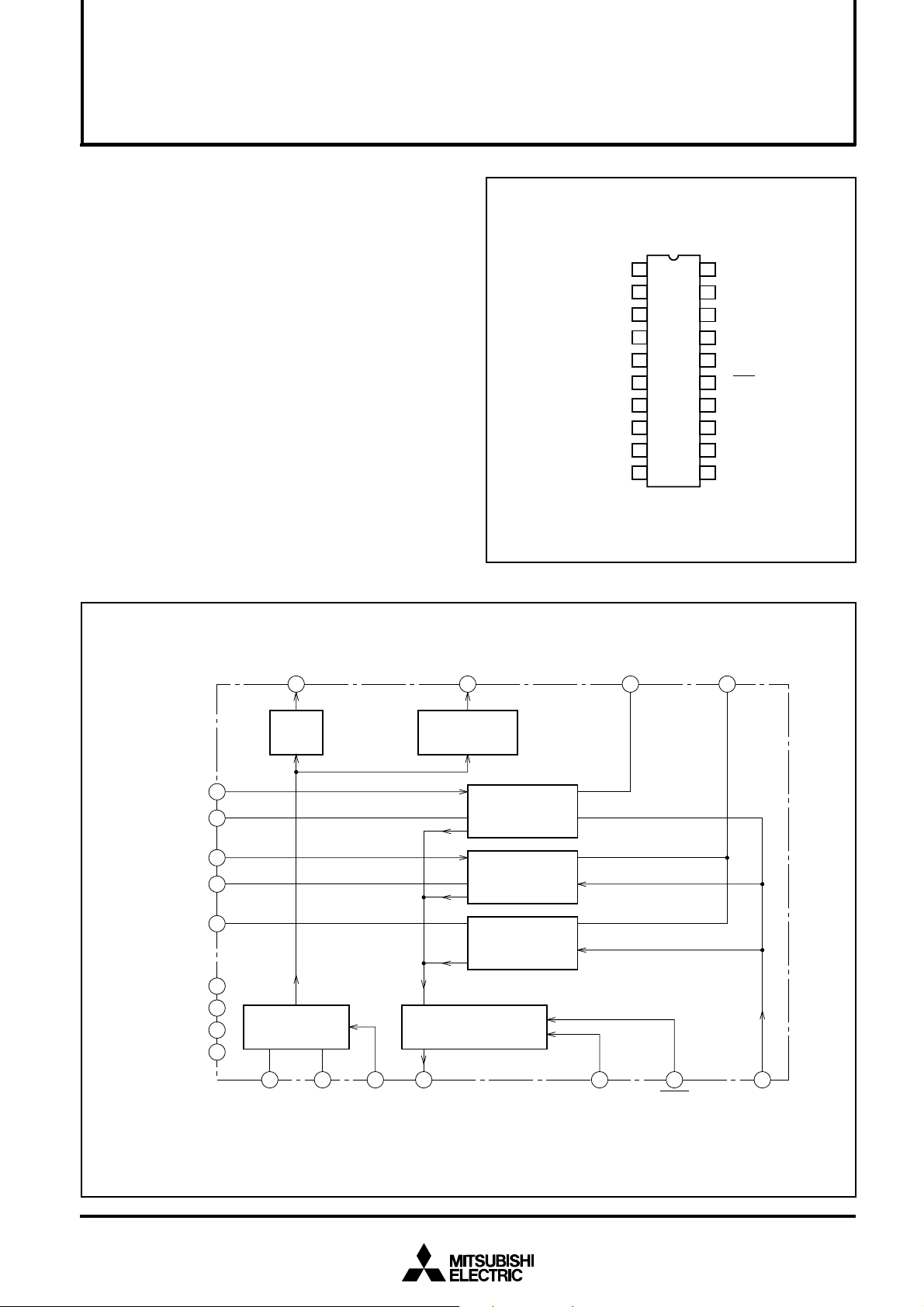
PIN CONFIGURATION (TOP VIEW)
V
CC1
CURRENT SETTING
INPUT 1
CURRENT SETTING
LOAD OUTPUT 1
CURRENT SETTING
INPUT 2
CURRENT SETTING
LOAD OUTPUT 2
LASER CURRENT
FORCED OFF INPUT
CURRENT SETTING
LOAD OUTPUT 3
GND1
MONITOR
LOAD INPUT 1
MONITOR
LOAD INPUT 2
1
→
VL1
2
←
1RC
3
→
VL2
4
←
2RC
5
→
V
OFF
6
←
3RC
7
8
→
1RM
9
→
2RM
10
Outline 20P4K
20
19
18
M66510P/FP
17
16
15
14
13
12
11
M66510P/FP
→
→
→
←
←
→
→
←
LASER CURRENT
1RO
LOAD OUTPUT 1
LASER CURRENT
2RO
LOAD OUTPUT 2
LASER DIODE
LD
OUTPUT
GND2
MONITOR DIODE
PD
INPUT
DATA
DATA INPUT
V
CC2
MONITOR
COMPARATOR
CO
OUTPUT
MONITOR ANALOG
MO
OUTPUT
DUTY
CD
CONTROL INPUT
BLOCK DIAGRAM
CURRENT
SETTING
INPUT 1
CURRENT
SETTING
INPUT 2
V
CC1
CC2
L1
L2
MONITOR OUTPUT
MO
12
LINEAR
AMPLIFIER
2
31RC
4V
52RC
73RC
1V
14V
DIFFERENTIAL AMPLIFIER
17GND2
8GND1
9
1RM102RM
VL1, 1RC: LASER CURRENT (IL1) SETTING PIN
V
L2
, 2RC: LASER CURRENT (IL2) SETTING PIN
3RC: LASER CURRENT (I
MONITOR
DIODE INPUT
COMPARATOR OUTPUT
CURRENT SWITCHING CIRCUIT
16
PD
18
LD
LASER
DIODE OUTPUT
L3
) SETTING PIN
CO
13
COMPARATOR
(V
ref
= 1.2V)
CONSTANT CURRENT
SOURCE (I
CONSTANT CURRENT
SOURCE (I
CONSTANT CURRENT
SOURCE (I
I
L = IL1 + IL2 + IL3
CC1
V
V
CC2
1RO
20
L1
Max. 60mA
Max. 30mA
Max. 30mA
)
L2
)
L3
)
11
CD
DUTY
CONTROL INPUT
, GND1: IC INTERNAL ANALOG POWER SUPPLY PIN
, GND2: IC INTERNAL DIGITAL POWER SUPPLY PIN
15
DATA
DATA INPUT
2RO
19
LASER CURRENT
FORCED OFF
6
V
OFF
1
MITSUBISHI 〈DIGITAL ASSP〉
M66510P/FP
LASER-DIODE DRIVER
FUNCTION
The 66510 is a semiconductor laser diode driver that drives a
semiconductor laser of the type (our R type) whose cathode
and the anode of monitor photodiode are connected to the
stem. Using the R type laser allows direct fixing the laser on
a device for easy installation, thus improving its radiation efficiency.
Laser driving current is set by applying voltage from outside.
The M66510 is equipped with two independent voltage applying pins to provide higher accuracy of setting the current
value.
PIN DESCRIPTIONS
Pin name
LD
PD
VL1
1RC
VL2
2RC
3RC
DATA
1RM,
2RM
MO
CO
VOFF
1RO
2RO
CD
VCC1
VCC2
GND1
GND2
Laser connecting pin
Monitor diode connecting pin
Voltage input pin for IL1 setting
Load resistor connecting pin for IL1
setting
Voltage input pin for IL2 setting
Load resistor connecting pin for IL2
setting
Load resistor connecting pin for IL3
setting
Switching data input pin
Monitor load resistor connecting pin
Monitor analog output pin
Monitor comparator output pin
Laser current forced off input pin
Load resistor connecting pin for laser
current IL1
Load resistor connecting pin for laser
current IL2/IL3
Duty compensating capacitor
connecting pin
Power supply pin 1
Power supply pin 2
GND pin 1
GND pin 2
Name
Connects the anode of semiconductor laser diode.
Connects the cathode of monitor photodiode.
Voltage input for setting the output current (IL1) of current source 1.
Connects IL1 setting load resistor between the pin and GND.
Voltage input for setting the output current (IL2) of current source 2.
Connects IL2 setting load resistor between the pin and GND.
Connects IL3 setting load resistor between the pin and GND. If IL3 is not used,
open the pin.
Turns on the laser in the “L” position, and off in the “H” position.
Connects between 1RM and 2RM the load resistor for converting monitor
photodiode current into voltage.
Analog output for monitoring laser power.
Comparator output for monitoring laser power.
Turns off all current source circuits in the “L” position.
Connects load resistor for laser current IL1 between 1RO pin and VCC.
Connects load resistor for laser current IL2 and IL3 between 2RO pin and VCC.
Connects duty compensating capacitor of optical output switch waveforms
between the pin and GND. If duty compensation is not required, open the pin.
Power supply for internal analog circuits. Connected to positive power supply
(+5V).
Power supply for internal digital circuits. Connected to positive power supply
(+5V).
GND for internal analog circuits.
GND for internal digital circuits.
It is also equipped with a laser current forced off pin to prevent overcurrent from flowing into the laser diode at the
power-ON time.
For detection of laser power, the monitor current of monitor
photodiode built in the laser is converted into voltage by an
external resistor to generate an analog output, and simultaneously the result of comparison with the internal reference
voltage is output as TTL-level logic information.
Function
2
MITSUBISHI 〈DIGITAL ASSP〉
M66510P/FP
LASER-DIODE DRIVER
DESCRIPTION OF OPERATION
1. Setting laser driving current
The M66510 is provided internally with three constant current
sources IL1, IL2 and IL3, allowing setting of each independent
output current.
The methods of setting IL1 to IL3 are given below in (1) to (3).
(1) Method of setting IL1
IL1 is approximated by the VL1 pin input voltage and the resistor (RC1) connected between 1RC pin and GND as follows:
L1[V]
IL1[mA] = 12 ×
V
RC1[kΩ]
However, 0≤ VL1 ≤ VCC – 1.8V, IL1(max.) = 60mA
(2) Method of setting I
L2
IL2 is approximated by the VL2 pin input voltage and the resistor (RC2) connected between 2RC pin and GND as follows:
L2[V]
IL2[mA] = 6 ×
However, 0≤ V
L2 ≤ Vcc – 1.8V, IL2(max.) = 30mA
V
RC2[kΩ]
(3) Method of setting IL3
IL3 is approximated by the internal reference voltage (Vref)
and the resistor (RC3) connected between 3RC pin and GND
as follows:
ref[V]
IL3[mA] = 10 ×
V
RC3[kΩ]
However, Vref=1.2V (standard), IL3(max.) = 30mA
Note: The expressions for setting IL1 to IL3 are typical. Actually, the set values
fluctuate several % depending on IC lot dispersion or operating ambient
temperature (See the ELECTRICAL CHARACTERISTICS).
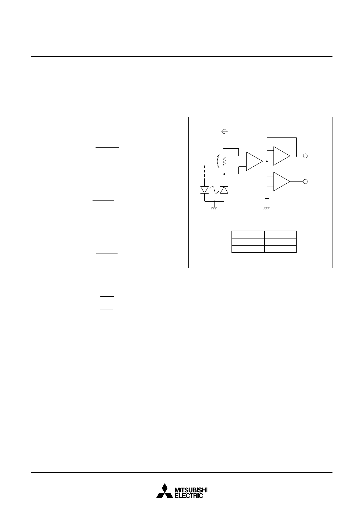
(2) The VM is output as an analog output from the MO pin
through the buffer amplifier and compared to the internal reference voltage Vref (1.2V standard) by the comparator. Then
the result of comparison is output from the CO pin on the TTL
level.
ref
–
+
Buffer
amplifier
+
–
Comparator
CO output
“L”
“H”
CO output
LD
V
M
RM
+ MO output
–
Differential
amplifier
PD
V
Condition
VM < Vref
VM > Vref
Monitor circuit schematic drawing
2. Switching operation
The laser is turned on when DATA= “L”. At this time, the laser driving current is I
L1 +IL2 +IL3.
The laser is turned off when DATA = “H”. At this time, the laser driving current becomes almost 0 regardless of IL1 to IL3.
3. Usage of VOFF input
The current which flows into the laser becomes 0 when
DATA= “H”. And the laser is turned off but the internal current sources are active.
Contrarily, the internal current sources are turned off when
OFF = “L”. It is therefore possible to prevent overcurrent from
V
flowing into the laser by setting V
OFF input to “L” until VCC
reaches 3.5V (standard) at the power-ON time, for example
(See 6. Internal reset).
4. Laser power monitor operation
The M66510 outputs the information on monitor photodiode
(PD) built in the laser from the MO and CO pins in the flow
given below.
(1) The current equal to the PD current produced through
emission of the laser flows into the resistor (RM) connected
between 1RM and 2RM. The potential difference (V
M) pro-
duced on RM is converted into a level from GND by the internal differential amplifier.
3

MITSUBISHI 〈DIGITAL ASSP〉
M66510P/FP
LASER-DIODE DRIVER
5. 1RO/2RO pin
The 1RO pin is used to connect the load resistor (RO1) for
current source 1 (I
load resistor (RO2) for current sources 2 (I
L1). The 2RO pin is used to connect the
L2) and 3 (IL3).
Connecting the load resistor between each pin and Vcc reduces IC internal power dissipation.
Set a resistance value so that each pin voltage does not go
down to 3.5V or less. In other words, set a value such as
meets the following expression:
RO1(RO2)[Ω] ≤
CC – 3.5[V]
V
Maximum load current [A] flowing into RO1(RO2)
Ex: When VCC = 5V and maximum load current of each source is 60mA, RO1
and RO2 will be 25Ω or less.
6. Internal reset operation
The M66510 is provided with an internal reset circuit to prevent overcurrent from flowing into the laser at the power-ON
time. The reset circuit operates within the range of V
CC <
3.5V (standard) to turn off all the current sources.
CC/GND pin
7. V
The power supply pins include V
CC1, VCC2, GND1 and
GND2, each of which is as follows in terms of internal circuit:
VCC1/GND1: Connected to an analog circuit.
CC2/GND2: Connected to a digital circuit.
V
In actual wiring, pay attention to the following:
(1) Make wiring width as wide as possible. Avoid redundant
wiring.
(2) Lay out an electrolytic capacitor for stabilizing voltage as
close to V
(3) Lay out a bypass capacitor as close to V
CC1/GND1 as possible.
CC2/GND2 as
possible.
Method of calculating power dissipation
The power dissipation P of M66510 is given by the expression given below.
CC × VCC +I(1RO) × (V(1RO) –V(LD))+I(2RO)× (V(2RO) –
P=I
V
(LD))+IOL(CO) × VOL(CO)
where, V(1RO) : 1RO pin voltage
(2RO) : 2RO pin voltage
V
I
(1RO) : 1RO pin load current
(2RO) : 2RO pin load current
I
(LD) : LD pin voltage
V
I
OL(CO) : CO pin “L” output current
OL(CO) : CO pin “L” output voltage
V
For example, when V
I
(1RO) =I(2RO) = 60mA, V(LD) = 2.5V, IOL(CO) = 8mA and
OL(CO) = 0.5V, the power dissipation at the laser-ON/OFF
V
CC = 5.25V, V(1RO) =V(2RO) = 3.5V,
time is as follows:
(1) Laser-ON time (DA TA = “L”, I
ON = 26 × 5.25 + 60 × (3.5 – 2.5) + 60 × (3.5 – 2.5) + 8 × 0.5
P
CC=26mA)
= 260.5(mW)
(2) Laser-OFF time (DATA = “H”, ICC = 44mA)
OFF = 44 × 5.25 + 0 + 0 + 8 × 0.5 = 235(mW)
P
Precaution for peripheral element wiring
Lay out the peripheral elements required for M66510 operation as close to M66510 as possible.
4

OPERATING WAVEFORM
P0
Laser output P
lL3
MITSUBISHI 〈DIGITAL ASSP〉
M66510P/FP
LASER-DIODE DRIVER
Laser output
Laser current lL
lL1
L2
l
Driving current pulse
lL1 : 0 ~ 60mA
l
L2 : 0 ~ 30mA
l
L3 : 0 ~ 30mA
ABSOLUTE MAXIMUM RATINGS
Symbol
VCC
VI
VO
IL1
IL2
IL3
Pd
Tstg
Note 1: When Ta ≥ 25°C, do derating of 10.4mW/°C.
2: When T
Supply voltage
Input voltage
Output current
Output current 1
Output current 2
Output current 3
Power dissipation
Storage temperature
a ≥ 25°C, do derating of 6.4mW/°C.
Parameter
VL1, VL2
DATA, VOFF
CO
1RO, 2RO
DIP
SOP
RECOMMENDED OPERATINIG CONDITIONS
Parameter
VCC
IL1
IL2
IL3
Topr
Symbol
Supply voltage
Output current 1
Output current 2
Output current 3
Operating ambient temperature
Conditions
When output is “H”
IC unit, when Ta=25°C (Note 1)
IC unit, when Ta=25°C (Note 2)
Conditions
Min.
4.75
–20
Ratings
–0.5 ~ +7.0
–0.3 ~ VCC
–0.3 ~ + 7
–0.3 ~ + 5.5
–0.3 ~ + 7
–90
–45
–45
1300
800
–65 ~ 150
Limits
Typ.
5
Max.
5.25
–60
–30
–30
75
Unit
V
V
V
mA
mA
mA
mW
°C
Unit
V
mA
mA
mA
°C
5

MITSUBISHI 〈DIGITAL ASSP〉
ELECTRICAL CHARACTERISTICS (VCC = 5V ± 5%, Ta = –20 ~ 75°C, unless otherwise noted)
Parameter
DAT A, VOFF
DAT A, VOFF
VL1, VL2
CO
CO
LD
MO
MO
Temperature coefficient
DAT A, VOFF
VIH
VIL
VI
VOH
VOL
VLD
VOS
∆VM
II
Symbol
“H” input voltage
“L” input voltage
Upper limit of effective input voltage
“H” output voltage
“L” output voltage
Operating supply voltage
Output offset voltage
Output voltage variance
width
Input current
VL1, VL2
Vref
IL1
IL2
IL3
IOFF
ICC
Note 3: IMO: MO pin output current. IPD: PD pin input current
4: RM: Resistance connected between 1RM and 2RM pins.
5: This indicates the input voltage – output current conversion characteristic. Use I
tions.
*: The standard value is given on VCC = 5V and at Ta = 25°C. The items with Ta specified under test conditions are given on VCC = 5V.
Reference voltage
Output current 1 (Note 5)
Output current 2 (Note 5)
Output current 3 (Note 5)
Off-state output current
Supply current
Temperature coefficient
LD
Temperature coefficient
LD
Temperature coefficient
LD
LD
Test conditions
IOH=–400mA
IOL=4mA
IOL=8mA
IMO=±20mA, IPD=0mA (Note 3)
IPD=–0.2~2.0mA, IMO=±20mA,
RM=1kΩ (Note 4)
RM=1kΩ, IPD=–1.2mA
VI=2.7V
VI=0.4V
VI=0~VCC
Ta=–20~75°C
Ta=25~75°C
VL1=3V, RC1=560 Ω, VLD=2V
VL2=3V, RC2=560 Ω, VLD=2V
RC3=360Ω, VLD=2V
VOFF=DATA=2V
VOFF=DATA=0.8V
VCC=5.25V, V
VL1=VL2=3.0V ,
OFF
=4.5V ,
DATA=0V
RC1=RC2=560Ω,
RC3=360Ω,
1RO, 2RO, LD open
L1 to IL3 within the range of limits of the recommended operating condi-
DATA=4.5V
Min.
2
VCC–1.8
2.7
0
VCC–1.4
M66510P/FP
LASER-DIODE DRIVER
Limits
Typ.*
30
20
0.05
1.2
–1.1
–0.7
–62
0.037
–31
0.017
–31
–0.2
–1
17
30
Max.
0.8
0.4
0.5
2.5
–0.2
–20
20
±1
–1
26
44
Unit
mV
mV
mV/°C
mA
mA
mA
mV/°C
mA
mA/°C
mA
mA/°C
mA
mA
mA
mA
V
V
V
V
V
V
V
ELECTRICAL CHARACTERISTICS (VCC = 5V, Ta = 25°C)
Test pin
Input
VL1/VL2
voltage
PD current
PD current
V
OFF
voltage
V
OFF
voltage
Output
current
voltage
voltage
LD current
LD current
6
fOP
tRP1
tRP2
tRP3
tON
tOFF
Symbol
Parameter
Operating frequency
Circuit response time 1
Circuit response time 2
Circuit response time 3
Circuit ON time
Circuit OFF time
LD
MO
CO
Test conditions
ILD(L)=0mA, ILD(H)=–60mA
(Note 6)
ILD(L)=–55mA,
ILD(H)=–65mA (Note 6)
IPD(L)=0mA, IPD(H)=–2mA,
RM=1kΩ (Note 7)
|∆IPD|=0.2mA, RM=1kΩ
(Note 7)
|∆IPD|=1mA (Note 7)
|∆IPD|=0.2mA (Note 7)
ILD(H)=–60mA (Note 8)
ILD(H)=–60mA (Note 8)
Min.
Limits
Typ.
20
4.5
0.5
7
1
7
0.5
3
0.5
Max.
7
2
10
3
10
2
5
2
Unit
Mbps
ms
ms
ms
ms
ms

MITSUBISHI 〈DIGITAL ASSP〉
M66510P/FP
LASER-DIODE DRIVER
NOTE 6: TEST CIRCUIT
NOTE 7: TEST CIRCUIT
5V
P.G.
t
r
= tf = 6ns
Oscilloscope
(input)
560Ω
50Ω
560Ω
L1
V
V
L2
1RC
2RC
1RM
V
CC
DATA
1RO
2RO
LD
PD
20Ω
20Ω
l
LD
Current probe
Oscilloscope
(output)
560Ω
560Ω
RM
2RM
GND
Other pins are open.
TIMING CHART TIMING CHART
V
IH
V
L1, VL2
I
LD
t
RP1
50%
10%
90%
t
RP1
50%
V
IL
I
LD(H)
I
LD(L)
IPD
MO, CO
V
V
1RC
2RC
1RM
2RM
50%
t
RP2,
tRP3
V
L1
L2
GND
MO=10%
CO=1.5V
CC
1RO
2RO
DATA
PD
CO
MO
20Ω
20Ω
l
PD
Oscilloscope
(output)
50%
MO=90%
CO=1.5V
5V
Oscilloscope (input)
Current probe
50Ω
Other pins are open.
PD
I
|
I
||
PD
t
RP2,
tRP3
P.G.
tr = tf = 6ns
IPD(H)
|
IPD(T)( ✽)
IPD(L)
V
OH
VOL
NOTE 8: TEST CIRCUIT
560Ω
560Ω
Oscilloscope (input)
P.G.
t
r
= tf = 6ns
50Ω
TIMING CHART
V
OFF
I
LD
1.5V
OFF
t
V
V
1RC
2RC
1RM
2RM
V
10%
L1
L2
OFF
V
CC
GND
1RO
2RO
LD
PD
DATA
20Ω
1.5V
20Ω
LD
I
Current probe
Other pins are open.
ON
t
90%
5V
Oscilloscope
(output)
3V
0V
I
LD(H)
I
LD(L)
PD when CO output is inverted.
: I
✽
7

APPLICATION EXAMPLE
MITSUBISHI 〈DIGITAL ASSP〉
M66510P/FP
LASER-DIODE DRIVER
5V
0.1mF 0.22mF
RC1
560Ω
RC2
560Ω
RC3
360Ω
M66510
L1
V
1RC
L2
V
2RC
3RC
V
CC1
V
CC2
GND2
GND1
12
Linear
amplifier
2
3
4
5
7
1
14
Differential amplifier
17
8
9
1RM102RM
RM
3kΩ
Control circuit
MO
16
CO
13
Comparator
(V
ref
= 1.2V)
Constant current source
(IL1)
Max. 60mA
Constant current source
L2
)
(I
Max. 30mA
Constant current source
L3
)
(I
Max. 30mA
Power supply switching
circuit
L
= I
L1
+ I
L2
I
18
PD
LD
ML4403R
5V
RO1
20Ω
1RO
20
+ I
L3
11
15
CD
91pF
Data stream Control signal
20Ω
DATA
RO2
2RO
19
6
V
OFF
8

STANDARD CHARACTERISTICS (VCC = 5V, Ta = 25°C)
MITSUBISHI 〈DIGITAL ASSP〉
M66510P/FP
LASER-DIODE DRIVER
LASER CURRENT - CURRENT SETTING VOLTAGE CHARACTERISTIC
–100
I
L1
+ l
L2
(mA)
L2
, I
L1
–80
–60
IL1(RC1=560Ω)
IL2(RC2=560Ω)
–40
LASER CURRENT I
–20
0
012
CURRENT SETTING INPUT VOLTAGE VL1, V
345
L2
(V)
MO OUTPUT - MONITOR CURRENT CHARACTERISTIC
LASER CURRENT - RC3 RESISTANCE CHARACTERISTIC
–50
–40
(mA)
L3
–30
–20
LASER CURRENT I
–10
0
0.2 0.4 0.6
RC3 RESISTANCE (kΩ)
0.8 1.0 1.2
CO OUTPUT - MONITOR CURRENT CHARACTERISTIC
5
(V)
MO
4
3
2
1
MONITOR ANALOG OUTPUT V
0
0–1–2
MONITOR CURRENT I
V
MO
RM=1kΩ
–3 –4 –5
PD
(mA)
(V)
5
CO
4
3
2
1
MONITOR COMPARATOR OUTPUT V
0
–0.8 –1.0 –1.2
MONITOR CURRENT I
–1.4 –1.6 –1.8
RM=1kΩ
PD
(mA)
9

EVALUATION OF SWITCHING OPERATION WAVEFORM
Connector
0.1mF
1
VCC 1VCC1
2GND
3VL1
4VL2
5VOFF
6GND
7CO
8MO
9DATA
10PD
22mF
JP
(Open)
RM
3kΩ
RC1
680Ω
RC2
680Ω
RC3
390Ω
2VL1
3 1RC
4V
L2
5 2RC
OFF
6V
7 3RC
8 GND1
9 1RM
10 2RM
CC2
MITSUBISHI 〈DIGITAL ASSP〉
M66510P/FP
LASER-DIODE DRIVER
RO
12Ω
201RO
192RO
18LD
17GND
16PD
15DATA
14V
13CO
12MO
D
11C
91pF
0.1
mF
( ✽ )
R
LD
500Ω
( ✽ )
CLD
75pF
Directly mounted on
PC board
Laser beam
output
ML4403R
V
CC = 5V
T
a = 25°C
Laser power
meter
50Ω
Oscilloscope
(laser beam output)
Oscilloscope (data input)
P.G.
(Note 9)
Note 9: tr =tf= 6ns, VO =3Vp-p, duty = 50%
50Ω
SWITCHING OPERATION WAVEFORM
DATA input
(2V/div)
Laser beam output
(1mW/div)
3V
0V
3mW
0mW
✽ : The R
LD and CLD optimum values depend on
a type of laser used and a PCB pattern.
EVALUATION CIRCUIT
2Mbit/s (t: 200ns/div)
10Mbit/s (t: 50ns/div) 20Mbit/s (t: 20ns/div)
5Mbit/s (t: 100ns/div)
10
Note: The delay from DATA input to laser beam output includes a measurement delay.
 Loading...