Mitsubishi M66503ASP Datasheet

MITSUBISHI 〈DIGITAL ASSP〉
MITSUBISHI 〈DIGITAL ASSP〉
16-BIT CONSTANT CURRENT LED DRIVER with SHIFT REGISTER AND LATCH
16-BIT CONSTANT CURRENT LED DRIVER with SHIFT REGISTER AND LATCH
DESCRIPTION
The M66503A is a constant current LED driver IC, whose
output current is variable. The IC’s functions include 16-bit
serial input/parallel output shift register with output latch.
The product uses Bi-CMOS process for highly accurate constant current driving, permitting high-efficiency LED driving
without using a resistor that limits LED current.
Settings for the LED drive current are made by an external resister, thereby ensuring a maximum output current of 30 mA,
enough for anode-common LED driving.
Furthermore, the pin configuration of the IC permits easier
wiring on a printed board.
FEATURES
• Anode-common LED driving
• Constant current output: Set to a value within a range between 0 and 30mA with an external resistor only.
Simultaneous lighting available.
• Pins (OE
A, OEB) provided for forced ON/OFF of LED drive
current.
• Greater noise margin: Total-input Schmitt circuit is employed to deal with longer wire lengths.
• Input/output CMOS compatible
• Serial data output provided (SQ15)
• 5V single power supply
• Pin configuration for easier wiring on printed board
APPLICATION
LED array drivers for display panel and printer. Other various
LED modules.
FUNCTION
The M66503A is a constant current LED driver for anodecommon LEDs. To set the LED driving current, an external
resistor is connected between the current setting input pin,
RC, and GND. In this way it is possible to set a highly accurate drive current. Each bit of the shift register is made up of a
flip-flop performing shift function and a latch connected to the
output. When the clock input pin, CK
S, goes from “L” to “H”,
data is shifted. Serial data is entered to the shift register via
the serial data input pin, A. Data on A is straight shifted. By
turning the latch enable input pin, LE, to “L”, the contents
stored in the shift register is latched. All outputs are turned of f
if the output enable input pins, OE
A and OEB, are simulta-
neously set to “L”. This function is useful for the prevention of
an excessive current flowing at the moment of power on. All
outputs are turned on if the OE
A pin is set to “H”. This enables
to check LEDs for failure. In these actions, changing the state
A and/or OEB does not affect the shift function. To ex-
of OE
pand the number of bits, link the M66503A in serial using the
serial data output pin, SQ15, which is the serial data output
of the shift register.
M66503ASP/AGP
M66503ASP/AGP
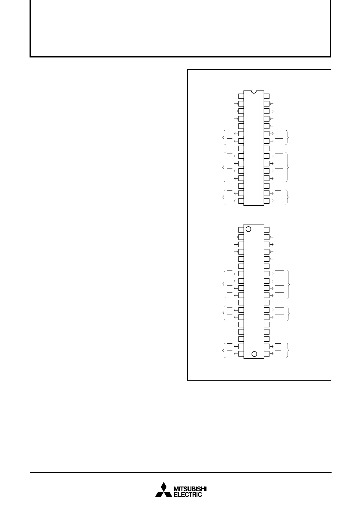
PIN CONFIGURATION (TOP VIEW)
GND1
CK
INPUT
GND2
GND3
GND1
CK
INPUT
GND2
LE
NC
Q
Q
Q
Q
Q
Q
Q
Q
LE
NC
NC
Q
Q
Q
Q
Q
Q
NC
NC
NC
Q
Q
A
S
0
1
2
3
4
5
6
7
A
S
0
1
2
3
4
5
6
7
SERIAL DATA INPUT
SHIFT CLOCK INPUT
LATCH ENABLE
PARALLEL DATA
OUTPUT
PARALLEL DATA
OUTPUT
PARALLEL DATA
OUTPUT
SERIAL DATA INPUT
SHIFT CLOCK INPUT
LATCH ENABLE
PARALLEL DATA
OUTPUT
PARALLEL DATA
OUTPUT
PARALLEL DATA
OUTPUT
1
2
3
4
5
6
7
8
9
10
11
12
13
14
15
Outline 30P4B
1
2
3
4
5
6
7
8
9
10
11
12
13
14
15
16
17
18
Outline 36P2R-D
30
29
28
27
26
25
M66503ASP
24
23
22
21
20
19
18
17
16
36
35
34
33
32
31
30
M66503AGP
29
28
27
26
25
24
23
22
21
20
19
V
CC
RC
SQ15
OE
A
OE
B
Q
15
Q
14
GND5
Q
13
Q
12
Q
11
Q
10
GND4
Q
9
Q
8
CC
V
RC
SQ15
OE
A
OE
B
NC
Q
15
Q
14
Q
13
12
Q
GND3
Q
11
10
Q
NC
NC
NC
Q
9
Q
8
NC: No Connection
CURRENT SETTING INPUT
SERIAL DATA OUTPUT
OUTPUT ENABLE INPUT A
OUTPUT ENABLE INPUT B
PARALLEL DATA
OUTPUT
PARALLEL DATA
OUTPUT
PARALLEL DATA
OUTPUT
CURRENT SETTING INPUT
SERIAL DATA OUTPUT
OUTPUT ENABLE INPUT A
OUTPUT ENABLE INPUT B
PARALLEL DATA
OUTPUT
PARALLEL DATA
OUTPUT
PARALLEL DATA
OUTPUT
1

OUTPUT
MITSUBISHI 〈DIGITAL ASSP〉
M66503ASP/AGP
16-BIT CONSTANT CURRENT LED DRIVER with SHIFT REGISTER AND LATCH
LECKSGND5GND4GND3GND2GND1VCCAOEBOEARC
LATCH ENABLE
INPUT
LED
1
CKD
1
PARALLEL DATA OUTPUT (Note 1) SERIAL DATA
LED
1
LED
1
LED
1
LED
1
LED
1
LED
1
LED
1
LED
1
LED
1
LED
1
CKD
1
CKD
1
CKD
1
CKD
1
CKD
1
CKD
1
CKD
1
CKD
1
CKD
1
CKD
1
SHIFT CLOCK
INPUT
(Note 2)
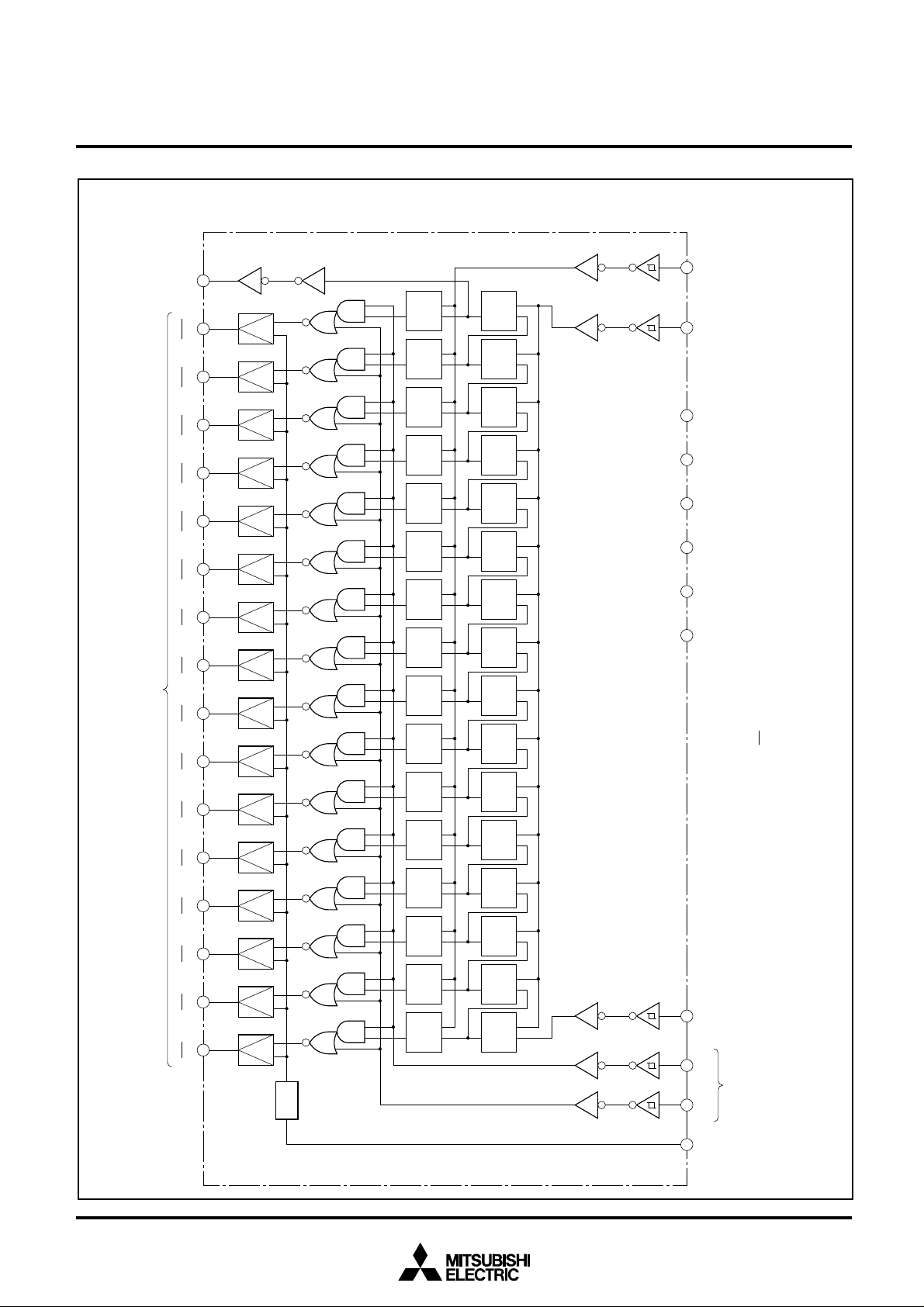
O(Qn) =5 · VCC/(2 · RC+100)
Note 1: Output current is approximated by the following equation.
I
2: GND 1 : for internal digital circuits
GND 2-5: for internal analog circuits
BLOCK DIAGRAM
2
LED
1
LED
1
LED
1
LED
1
LED
1
Q0 Q1 Q2 Q3 Q4 Q5 Q6 Q7 Q8 Q9 Q10 Q11 Q12 Q13 Q14 Q15 SQ15
∗1
∗2
CKD
1
CKD
1
CKD
1
∗1: constant current driver
CKD
1
CKD
1
∗2: Regulator
SERIAL DATA
INPUT
OUTPUT ENABLE
INPUT
CURRENT
SETTING
INPUT

FUNCTION TABLE (Note 3)
Input Parallel output
CKS
LE
A
OEA
OEB
Q0
↑
H
H
L
H
L
↑
H
L
L
H
Z
X
L
X
L
X
X
L
L
X
X
H
H
Note 3: ↑ :Denotes change from “L” to “H”.
0 :Denotes state of Q output before change in CKS input.
Q
x :Either “L” or “H”
q0:Contents of shift register before change in CKS input
q :Contents of shift register
z :Denotes high impedance state
0
H
Q0
L
Z
X
L
PIN DESCRIPTION
Pin
A
CKS
LE
OEA
OEB
SQ15
RC
Qn
VCC
GND1
GND2~5
Name
Serial data input pin
Shift clock input pin
Latch enable input pin
Output enable input
pins
Serial data output pin
Current setting input pin
LED connection pins.
Power supply pin
GND pin 1
GND pins 2-5
MITSUBISHI 〈DIGITAL ASSP〉
M66503ASP/AGP
16-BIT CONSTANT CURRENT LED DRIVER with SHIFT REGISTER AND LATCH
Q1
0
Q0
0
Q0
0
Q1
Z
L
Input/Output
Q2
0
Q1
0
Q1
0
Q2
Z
L
Input
Input
Input
Input
Output
Input
Output
Q3
Q4
Q2
Q2
Q3
Q5
0
0
Q3
0
0
Q3
0
0
Q4
Z
Z
L
L
··································
0
Q4
··································
0
Q4
··································
0
Q5
··································
Z
··································
L
··································
Q12
Q11
Q11
Q12
0
0
0
Z
L
Q13
Q12
Q12
Q13
Q14
0
0
Q13
0
0
Q13
0
0
Q14
Z
Z
L
L
Description
Shift register’s serial data input pin.
Clock input pin. Shifts data at leading edge.
If “H”, contents in shift register appear at output Qn, and if “L”, contents in shift
register are latched.
Output enable input pins.
If OEA =“H”, all outputs, Qn, are turned on.
If OEA =“L” and OEB =“L”, all outputs, Qn, are turned off.
Serial data output pin of shift register
Connect a resistor between the RC pin and GND to set the driving current.
Driver output pins. Connect LED’s cathodes to these pins.
Connect to positive power source (+5V).
GND for internal digital circuits.
GND for internal analog circuits.
Q15
Q14
Q14
Q15
Z
L
Serial output
0
0
0
SQ15
q14
q14
q15
q15
q15
0
0
3
 Loading...