MITSUBISHI 〈DIGITAL ASSP〉
MITSUBISHI 〈DIGITAL ASSP〉
DESCRIPTION
The M66332 is a facsimile image processing controller that
converts analog signals that are photoelectrically converted
by an image sensor into bi-level signals.
It has image processing functions such as peak detection,
uniformity correction, γ correction, MTF compensation, detector of background and object levels, dither control, separation of image data area, scale down, and area specification.
This controller has a built-in 5-bit flash type A-D converter
and interface circuits to image sensor, analog signal processing circuit, and CODEC (Coder & Decoder) to simplify control
of the readout mechanism.
FEATURES
0High Speed Scan (MAX. 2 ms/line, TYP. 5 ms/line)
0A3 (8 pixels/mm) Line Sensor Attachment
0Image sensor (CCD,CIS) control signal generation
CCD: SH, CK1, CK2, RS
Contact sensor (CIS): SH, CK1 (or CK2)
M66332FP
FACSIMILE IMAGE DATA PROCESSOR
FACSIMILE IMAGE DATA PROCESSOR
M66332FP
0Analog signal processing circuit control signal generation
CLAMP, S/H, AGC, DSCH
0Built-in 5-bit Flash Type A-D Converter
0Bi-level data external input/output interface Serial output
(→M66330)
8-bit MPU bus output with external DMA control signal
0Image data processing
γ correction
Uniformity correction (block correction in units of 8 pixels)
MTF compensation (1 dimension)
Detector of background and object level (programmable)
Dithering control
• Dither method (16 levels using 4 × 4 matrix)
Separation of image data area (1 dimension)
Scale down A3 → B4, A3 → A4, B4 → A4
05V Single Power Supply
APPLICATION
Facsimiles
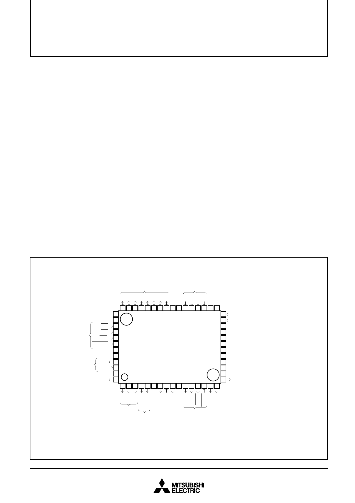
PIN CONFIGURATION (TOP VIEW)
45
GND
46
V
CC
CS
47
48
MPU Interface
DMA Interface
Sensor Interface
RD
WR
RESET
GND
GND
DRQ
DAK
V
CC
SH
49
50
51
52
53
54
55
56
MPU
Interface
(DATA)
D7D6D5D4D3D2D1
444342414039383736353433323130
D0
MPU
Interface
(ADDRESS)
GND
VCCA3A2A1A0DGND
M66332FP
123456789
RS
CK2
CK1
Sensor
S/H
CLAMP
Interface
Prosessing
Analog Signal
GND
TEST
Test pin
Interface
10111213141516
CC
V
SVID
TEST
SYSCK
Test pin
System clock
STIM
SCLK
CODEC
Interface
SRDY
Outline 56P6N-A
CC
DV
29
28
TEST
27
ASIG
26
NC
25
VWL
24
VML3
23
ML2
V
22
GND
21
VML1
20
BL
V
19
AGND
18
CC
AV
17
DSCH
AGC
PTIM
Interface
Processing
Analog Signal
Sensor Interface
Test pin
Analog Signal
Processing Interface
White Basic Supply Voltage
Middle Basic Supply Voltage 3
Middle Basic Supply Voltage 2
Middle Basic Supply Voltage 1
Black Basic Supply Voltage
Analog Signal
Processing Interface
NC: No Connection
1
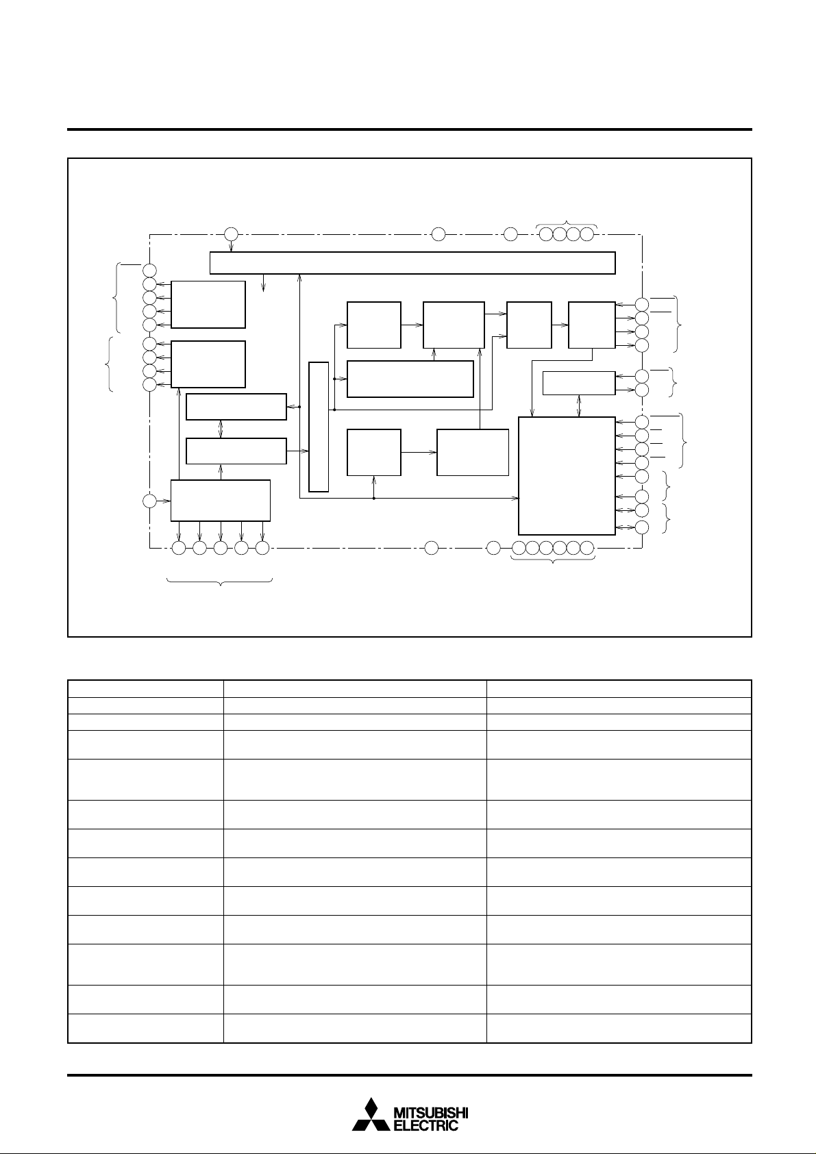
BLOCK DIAGRAM
MITSUBISHI 〈DIGITAL ASSP〉
M66332FP
FACSIMILE IMAGE DATA PROCESSOR
Sensor
Interface
Analog
Signal
Interface
ASIG
System Clock ADC Analog
SYSCK
15PTIM
56SH
2CK1
Sensor Control
1CK2
3RS
4CLAMP
5S/H
Analog Control
16AGC
17DSCH
Correction memory
(304 words × 5bits)
Uniformity Correction
5bit A-D converter
27
(flash type)
20
21
23
V
BL
V
ML2
V
ML1
ADC Reference Voltage
8
24
V
ML3
To each
block
25
V
WL
Vcc
AV
CC
18
Image Processing Sequence Control Signal
Detection
of Image
Data Area
Simple Bi-level
Conversion/Background
and object Level Detection
SRAM 16
words
× 4bits
MTF compensation
Separation
of Image
Data Area
Collective
Dithering
(16 levels)
AGND
ADC
Analog GND
ADC Logic
DV
DGND
ADC
Logic GND
Vcc
CC
29
Convert
bi-level
V
CC
10 35 46 55
to
DMA Control
MPU Bus Interface
GND
Cur out/
Scale
down
525145362263019
14 SRDY
13 STIM
12 SCLK
11 SVID
54 DAK
53 DRQ
50 RESET
47 CS
48 RD
49 WR
MPU
31 A0
~~
Interface
34 A3
(Address)
37 D0
MPU
Interface
44 D7
(Data)
CODEC
Interface
DMA
Interface
MPU
Interface
Table 1 Image Processing Functions
Image Processing Function
Read Width
Resolution
Read speed
Uniformity Correction
MTF Compensation
Simple Bi-level Conversion
Pseudo half-tone
Separation of Image Data
Area
Scale down
γ Correction
Image Sensor Control Signal
Analog Signal Processing
• A4, B4, A3
• 8 pixels/mm (primary scanning direction)
• 5ms/line Typ. 2ms/line maximum
• White correction only
• Block correction in units of 8 pixels
• 50% Correction range
• Laplacian filter circuit for 3 × 1 pixels in current line
(1 dimension)
• Floating threshold method using background and
object level detection circuit
• Dither method: 16 levels (4 × 4matrix)
• Detection by brightness difference in 5 × 1 pixels
area in current line
• Selection method • Scale down: A3 → B4 set
to 13/15; B4 → A4, 9/11; A3 → A4, 12/17
• Logarithmic correction
• Control signal generation for contact sensor (CIS)
and scale down CCD
• Generate control signals for external CLAMP
circuit, sample/hold circuit, and AGC circuit
Specifications
Remarks
• Operated with system clock and PRE_DATA
(registers 2, 3)
• Built-in SRAM as correction memory (304 words ×
5bits) (read/write allowed from MPU)
• No need for compensation memory
• Built-in SRAM as dither memory (16 words × 4bits)
(read/write allowed from MPU)
• No need for processing memory
• Apply external voltage (resistor connection is also
allowed) to A-D converter middle basic supply
voltage pins.
• Built-in 5-bit flash A-D converter
2

PIN DESCRIPTIONS
Block
Sensor Interface
Analog Circuit
Interface
CODEC Interface
DMA Interface
Clock
MPU Interface
Pin Names
SH
CK1
CK2
RS
PTIM
CLAMP
S/H
ASIG
AGC
DSCH
SRDY
STIM
SCLK
SVID
DRQ
DAK
SYSCK
RESET
CS
RD
WR
A0~A3
D0~D7
MITSUBISHI 〈DIGITAL ASSP〉
M66332FP
FACSIMILE IMAGE DATA PROCESSOR
I/O
CCD: Shift pulse signal to transmit photo charges from the sensor to the transfer unit.
O
CIS: Start signal for the sensor read circuit.
CCD: Clock pulse signal for sequentially transmitting the transfer unit signal charge of the
O
sensor.
CIS: Clock pulse signal for the sensor read circuit shift register.
Reverse of CK1.
O
Pulse to reset the voltage of the CCD sensor floating capacitor to initial status.
O
Read roller pulse motor control signal.
O
CLAMP pulse to set the dark level of the sensor to reference voltage of the digital circuit.
O
Sample-hold signal to smooth out sensor image signal waveform.
O
Analog signals.
I
External AGC circuit gain down signal.
O
External AGC circuit gain up signal.
O
Data transmission ready signal from CODEC.
I
Data transmission bound signal for CODEC.
O
Clock signal for transmitting image data to CODEC.
O
Serial output of image data to CODEC. “H”: Black; “L”: White.
O
DMA request signal to external DMA controller for parallel output of image data through MPU
O
bus.
DMA acknowledge signal from external DMA controller for the above DRQ signal.
I
System clock input pin.
I
System reset signal. Resets counter, register, F/F, and latch, sets internal memory in standby
I
mode, and halts clock generation circuit.
Chip select signal used by MPU to access M66332. Set to “H” in operating mode (AGC, UNIF,
I
SCAN).
Control signal used by MPU to read data from M66332.
I
Control signal used by MPU to write data to M66332.
I
Address signals used to access M66332 internal registers.
I
8-bit bidirectional buffer.
I/O
Description
3

PIN DESCRIPTIONS (CONTINUED)
Block
Others
Pin Names
VCC
AVCC
DVCC
GND
AGND
DGND
VWL
VBL
VML1
VML2
VML3
TEST(IN)
TEST(OUT)
I/O
––
––
––
––
––
––
––
––
––
––
––
––
––
MITSUBISHI 〈DIGITAL ASSP〉
M66332FP
FACSIMILE IMAGE DATA PROCESSOR
Description
Plus supply voltage.
Plus supply voltage for A-D converter analog units.
Plus supply voltage for A-D converter logic units.
GND pin.
Ground for A-D converter analog units.
Ground for A-D converter digital units.
A-D converter white basic supply voltage pin.
A-D converter black basic supply voltage pin.
Middle basic supply voltage pin. VML1 =(VWL – VBL) /4
Middle basic supply voltage pin. VML2 =2 ·(VWL – VBL) /4
Middle basic supply voltage pin. VML3 =3 ·(VWL – VBL) /4
Test input pin. Fix to “L”.
Test output pin. Keep open.
FUNCTIONAL DESCRIPTION
The following items which are necessary to use the image
processing functions of the M66332 are described.
(1)Operating mode
(2)Line period and read sequence
(3)Image processing function
(4)Sensor unit/analog signal processing unit interface
(5)CODEC interface
(6)Read/write to dither memory and uniformity correction
memory
(7) Reset
(8)Image quality control using registers
4

MITSUBISHI 〈DIGITAL ASSP〉
M66332FP
FACSIMILE IMAGE DATA PROCESSOR
(1)Operating mode
The M66332 performs three basic operations.
• Peak value detection: The peak value of the analog signal
output from the analog signal processing circuits is
matched to the white reference voltage (V
M66332 internal A-D converter. (See also Figs. 19 to 22 in
the M66333FP document.)
• Uniformity correction data creation: White reference data is
created for sensor unit uniformity correction and written to
the correction memory (SRAM: 304 words × 5bits).
• Read operation: A document is read and the image is processed to output bi-level data as serial or parallel output.
These three basic operations are performed in the following
sequence depending on whether the sensor is CCD or CIS.
The sensor is selected with register 0 (SENS).
When the sensor is CCD:
UNIF mode Operation is started by setting the
UNIF command in register 0 to “H”.
If the sensor is CCD, peak detection
(16 line periods) and white uniformity correction data creation (8 line
periods) are performed consecutively.
To exit this operating mode, wait 30
line periods (at least 24 lines) from
the start and set the UNIF command
to “L”.
v
SCAN mode The read operation is started by set-
ting the SCAN command in register
0 to “H”.
Set the SCAN command to “L” to exit
this operation mode.
WL) of the
When the sensor is CIS:
(Creation and transmission of uniformity correction data)
UNIF mode This mode is started when the UNIF
command in register 0 is set to “H”.
When the sensor is CIS, if white correction is started with the UNIF command, peak detection (16 line
periods) and uniformity white correction data creation (8 line period) are
started.
To exit this operating mode, wait 30
line periods (at least 24 line periods)
from the start and set the UNIF command to “L”.
v
Data transfer The uniformity correction data per-
taining to white correction created in
UNIF mode are transferred to the
backup memory.
(Read operation)
AGC mode Peak detection is performed for 16
line periods when the AGC command in register 0 is set to “H”.
To exit this operating mode, wait 20
line periods (at least 16 lines) from
the start and set the AGC command
to “L”.
v
SCAN mode The read operation is started by set-
ting the SCAN command in register
0 to “H”.
Set the SCAN command to “L” to exit
this operating mode.
The signal functions and data flow in each mode are shown
on pages 4–123 and 4–124. Flowcharts are shown on pages
4-158 to 4–160.
5
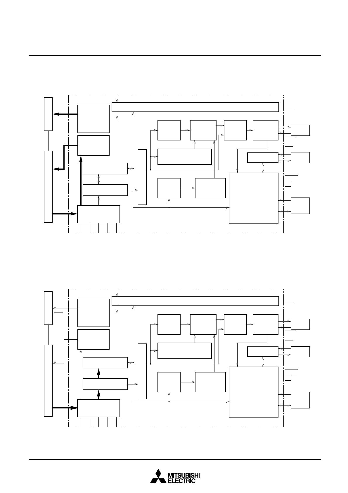
Operation During Peak Detection
MITSUBISHI 〈DIGITAL ASSP〉
M66332FP
FACSIMILE IMAGE DATA PROCESSOR
SYSCK
Image Processing Sequence Control Signal
PTIM
SH
Image sensorAnalog signal processing circuit
CK1
CK2
RS
CLAMP
S/H
AGC
DSCH
ASIG
Sensor Control
Analog Control
Correction memory
(304 words × 5bits)
Uniformity Correction
5bit A-D converter
(flash type)
VBL
VML2
VML1
VML3
To each
block
Resolution compensation
VWL
Data Flow in Creation of Uniformity Correction Data
Detection
of Image
Data Area
Simple Bi-level
Conversion/Background
and object level detection
SRAM 16
words
× 4bits
Separation
of Image
Data Area
Collective
Dithering
(16 levels)
Convert to
bi-level
DMA Control
MPU Bus Interface
Cut out/
Scale down
STIM
SCLK
SVID
CODEC
SRDY
DAK
DMA
DRQ
RESET
CS,RD
WR
A0~A3
MPU
D0~D7
SYSCK
PTIM
SH
Image sensorAnalog signal processing circuit
CK1
CK2
RS
CLAMP
S/H
AGC
DSCH
ASIG
Sensor Control
Analog Control
Correction memory
(304 words × 5bits)
Uniformity Correction
5bit A-D converter
(flash type)
VBL
VML2
VML1
VML3
To each
block
VWL
Image Processing Sequence Control Signal
Detection
of Image
Data Area
Simple Bi-level
Conversion/Background
and object level detection
SRAM 16
words
MTF Compensation
× 4bits
Separation
of Image
Data Area
Collective
Dithering
(16 levels)
Convert to
bi-level
DMA Control
MPU Bus Interface
Cut out/
Scale down
STIM
SCLK
SVID
CODEC
SRDY
DAK
DMA
DRQ
RESET
CS,RD
WR
A0~A3
MPU
D0~D7
6
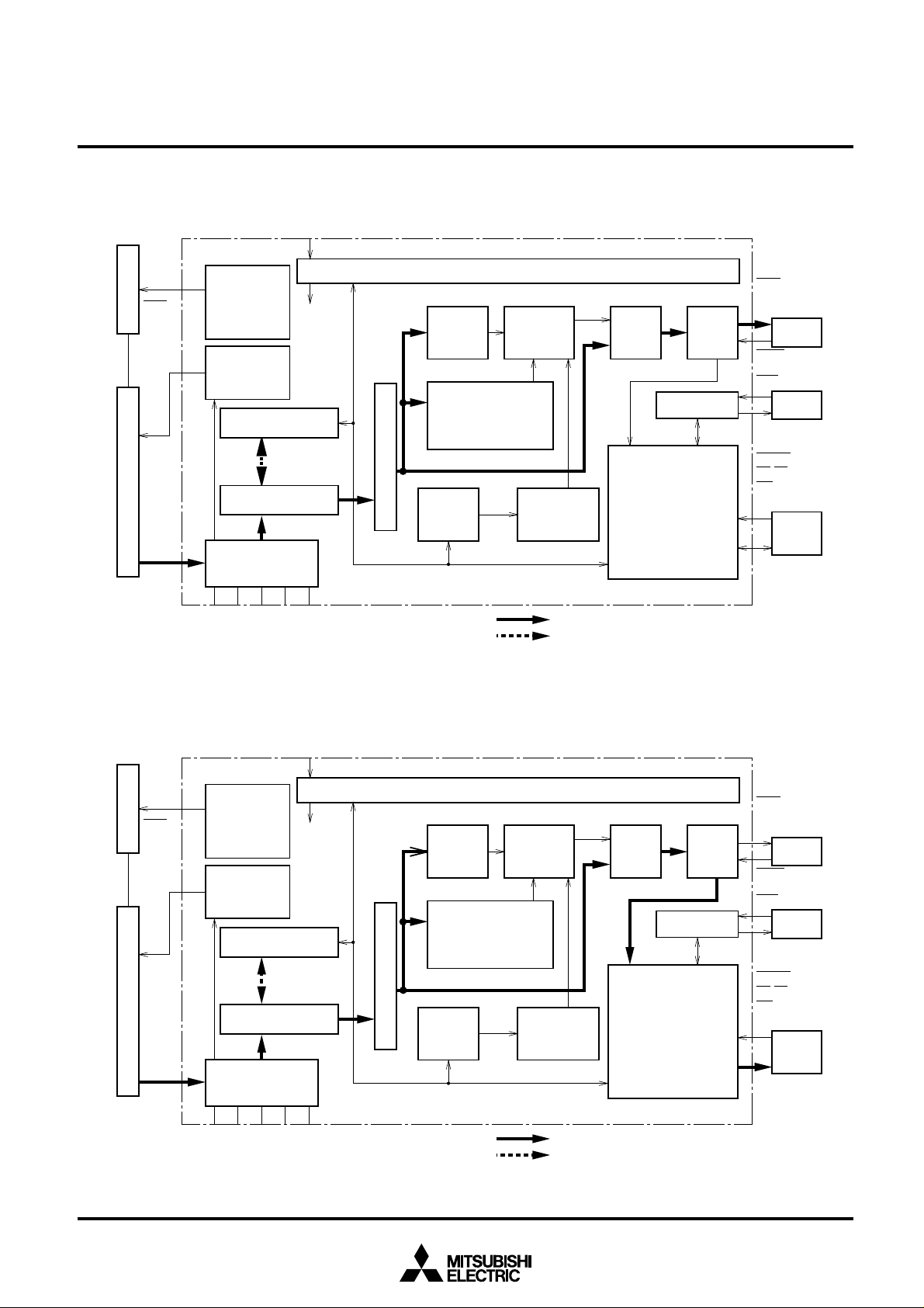
Date Flow During Read Operation (for serial output)
SYSCK
MITSUBISHI 〈DIGITAL ASSP〉
M66332FP
FACSIMILE IMAGE DATA PROCESSOR
Image Processing Sequence Control Signal
PTIM
SH
Image sensorAnalog signal processing circuit
CK1
Sensor Control
To each
block
CK2
RS
Analog Control
Correction memory
(304 words × 5bits)
CLAMP
S/H
AGC
DSCH
Uniformity Correction
SRAM 16
MTF Compensation
5bit A-D converter
V
BL
V
(flash type)
V
ML2
ML1
V
ML3
V
WL
ASIG
Date Flow During Read Operation (for parallel output)
Detection
of Image
Data Area
Simple Bi-level
Conversion/
Background
and object
level detection
words
× 4bits
Separation
Convert
of Image
Data Area
Collective
Dithering
bi-level
MPU Bus Interface
(16 levels)
: Image date
: Correction, Compensation date
to
Cut out/
Scale
down
DMA Control
STIM
SCLK
SVID
CODEC
SRDY
DAK
DMA
DRQ
RESET
CS,RD
WR
A0~A3
MPU
D0~D7
SYSCK
PTIM
SH
Image sensorAnalog signal processing circuit
CK1
Sensor Control
CK2
RS
Analog Control
Correction memory
(304 words × 5bits)
CLAMP
S/H
AGC
DSCH
Uniformity Correction
5bit A-D converter
V
BL
V
(flash type)
V
ML2
ML1
V
ML3
ASIG
To each
block
V
WL
Image Processing Sequence Control Signal
Detection
of Image
Data Area
Separation
of Image
Data Area
Simple Bi-level
Conversion/
Background
and object
level detection
SRAM 16
words
Resolution compensation
× 4bits
Collective
Dithering
(16 levels)
: Image date
: Correction, compensation date
Convert
to
bi-level
Cut out/
Scale
down
DMA Control
MPU Bus Interface
STIM
SCLK
SVID
CODEC
SRDY
DAK
DMA
DRQ
RESET
CS,RD
WR
A0~A3
MPU
D0~D7
7
MITSUBISHI 〈DIGITAL ASSP〉
M66332FP
FACSIMILE IMAGE DATA PROCESSOR
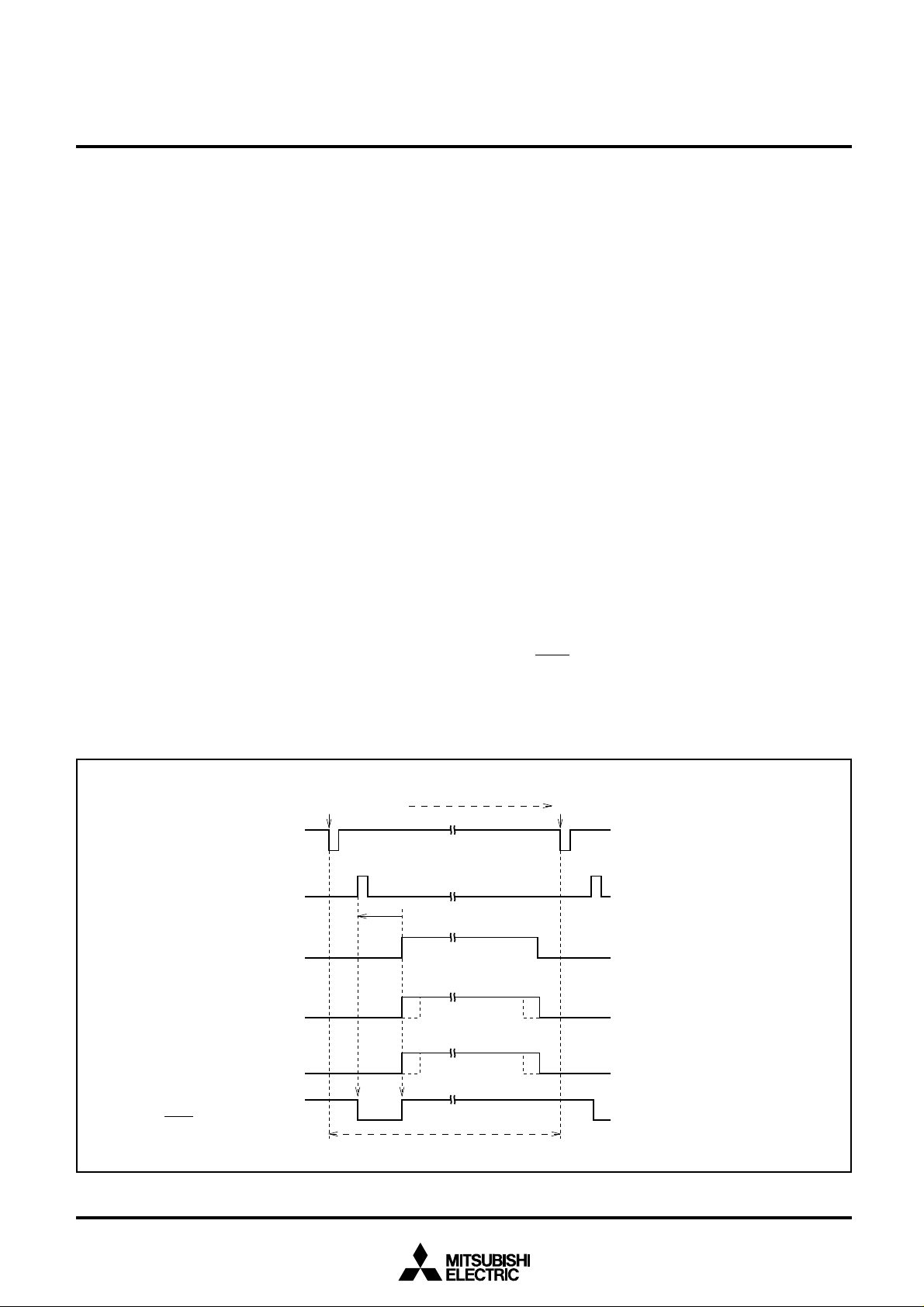
(2)Line period and read sequence
Figure 1 shows the relationship between the M66332 line
period and the read sequence.
• 1 line period (1/ACCK): Defines the processing time per
line for M66332. The line period is
determined from the line period
counter registers 2 and 3
(PRE_DATA) and pixel transmission clock (ADCK). ADCK is 1/
16th of SYSCK.
1 line period (1/ACCK) [NS]
= line period counter × pixel transmission clock period [NS]
= (PRE_DATA + 1) × 1/ADCK [NS]
= (PRE_DATA + 1) × 16/SYSCK [NS]
The line period counter is
counted down with the pixel
transmission clock after loading
the PRE_DATA value and generates the following addresses.
• Sensor start pulse (SH): Image sensor start pulse. The position of the start pulse is determined by the value in register 4
(ST_PL) which is the offset from
the uniformity correction range
(UNIFG).
Set ST_PL to the following values
according to the type of image
sensor.
CCD: ST_PL = sensor dummy
pixel + 2
CIS: ST_PL =2
• Uniformity correction
range (UNIFG):
• AGC range (AGCG):
• Source document read
width:
• Pulse motor control
signal (PTIM):
Defines the uniformity correction
range. This range corresponds to
the sensor width (A3 to A4).
Refer to Table 2 for the relationship between sensor width and
uniformity correction range.
Defines the peak detection range.
This range corresponds to the
sensor width (A3 to A4).
Auto gain control is performed for
the entire width (solid line) of the
sensor in AGC mode and for the
range inside the sensor width
(dotted line) in SCAN mode.
Refer to Table 2 for the relationship between sensor width and
AGC range.
Defines the source document
read width.
If the document width is less than
the sensor width, the document
should be centered on the sensor
because the read range is set
from the center of the sensor.
Refer to Table 3 for the relationship between sensor width and
source document read width.
Generates the pulse motor control signals for the read roller.
PRE_DATA load 0
Line period
(ACCK)
Sensor start
pulse
(SH)
Uniformity correction
range
(UNIFG)
AGC range
(AGCG)
Source document
read width
Pulse motor
control
(PTIM)
Fig. 1 Line period and read sequence
ST_PL
Down count
1 line period
Relationship with registers
Registers 2, 3
(PRE_DATA)
Register 0 (SENS_W)
Register 4 (ST_PL)
Register 0 (SENS_W)
Register 0 (SENS_W)
Register 1 (SOURCE)
Register 1
(SOURCE, DEST , REDU)
8
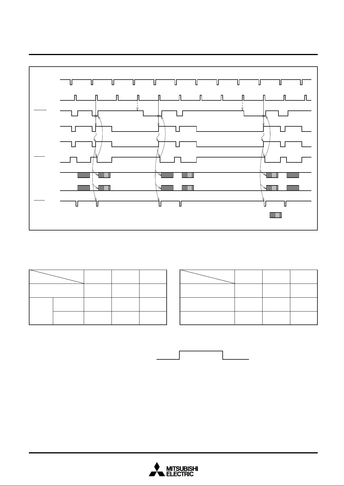
1 line period
(ACCK)
Sensor start
pulse (SH)
SRDY
(SSCAN)
(BCSCAN)
STIM
SCLK
MITSUBISHI 〈DIGITAL ASSP〉
M66332FP
FACSIMILE IMAGE DATA PROCESSOR
SVID
PTIM
Fig. 2 CODEC Interface and read sequence
Table 2 Sensor width and gate signal range
Sensor width
Gate signal
Uniformity correction
range (UNIFG)
AGC
range
(AGCG)
AGC mode
SCAN mode
A3
2487/55
2487/55
2370/162
2279/231
2279/231
2194/306
X : Left end address
Y : Right end address
B4
A4
2119/391
2119/391
1760/740
: Output bound(SSCAN), (BCSCAN) : Internal signals
Table 3 Source document read width according to
sensor width and source document size
Sensor width
Source document size
A3
B4
A4
XYX / Y
A3
2487/55
2278/230
2118/390
B4
––
2278/230
2118/390
2118/390
A4
––
––
9
MITSUBISHI 〈DIGITAL ASSP〉
M66332FP
FACSIMILE IMAGE DATA PROCESSOR
(3)Image processing function
The M66332 converts image signals from the image sensor
to bi-level signals. Bi-level conversion can be either simple bilevel conversion or pseudo half-tone conversion which converts image shades into bi-levels.
The signal output from the image sensor must be corrected
and compensated to reduce distortion and degradation before it can be converted to bi-level signals.
Furthermore, for reduction in transmission time, separation of
image data area and optimum bi-level conversion must be
performed.
The functions necessary for image processing are described
below.
• Peak detection
• Uniformity correction
• MTF compensation
• Background and object level detection (simple bi-level conversion)
• Pseudo half-tone
dither method
• Separation of image data area
• Image scale down/area specification
• Peak detection
The A-D converter of the M66332 is used with its reference
voltages (V
BL, is set to 0V to keep the dynamic range of the A-D con-
V
WL, VBL) fixed. Normallly, VWL is set to VCC and
verter wide. Peak detection must be performed for analog signals to match them with the full scale value of the A-D
converter before they are input to the A-D converter.
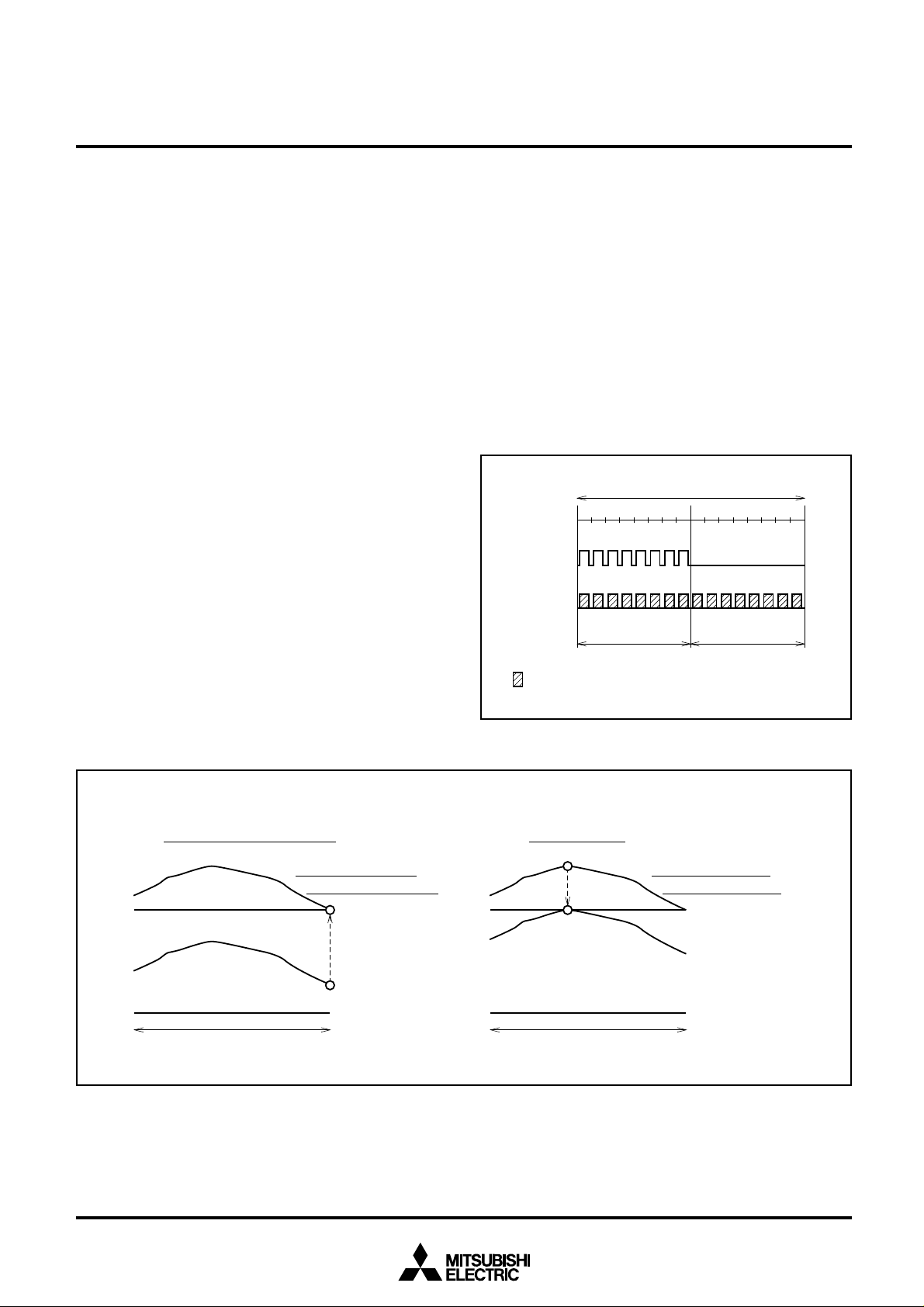
Peak detection is performed by reading white data in AGC
mode, one of the three M66332 operating modes (AGC,
UNIF, SCAN).
In AGC mode, 8-line period worth of DSCH signal to raise
gain—for gain control—and 16-line period worth of AGC signal to lower gain—for the overflowing of the A-D converter—
are generated after AGC command start (register 0: AGC) as
shown in Fig. 3.
This changes the gain as shown in Fig. 4.
Peak detection
Line period
DSCH
(raise gain)
AGC
A-D converter
overflow
(lower gain)
12345678910111213141516
Peak detection
preprocessing
Peak gain control
Peak detection (preprocessing)
After completing peak
detection preprocessing
V
WL
White data
V
BL
1 line
Match the output
level of the last pixel
of a line to V
Fig. 4 Changes in gain during peak detection
WL
: Generated in pixel units only when the A-D converter overflows.
Fig. 3 Peak detection
Peak gain control
V
WL
V
BL
1 line
After completing gain
control for peak value
Match the peak sensor
output within a line toV
WL
10
• Uniformity correction
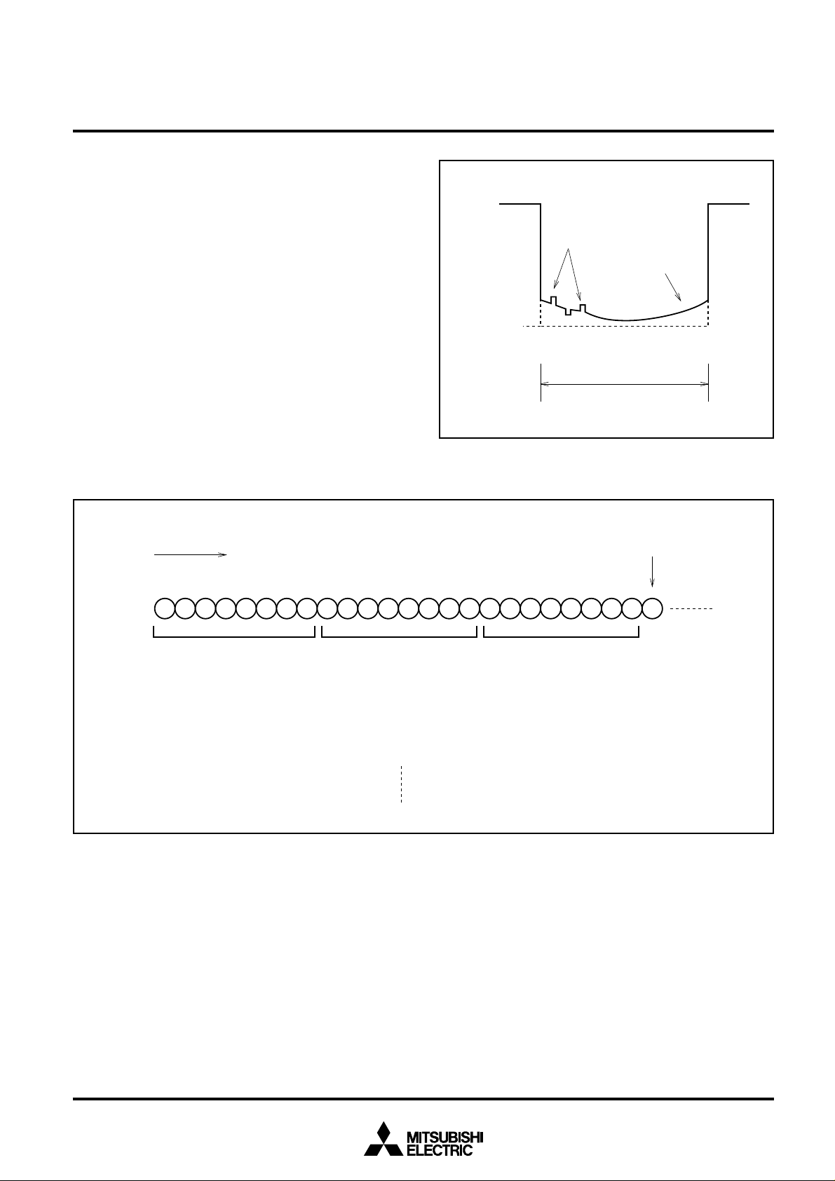
Uniformity correction corrects the drop in lighting level at
both ends of the light source, shading distortion due to drop
in lighting level at the rim of the lens, and high frequency distortion caused by the scattering of pixel-unit image sensor
characteristic (see Fig. 5).
The M66332 creates uniformity correction data in UNIF
mode, one of the three operating modes (AGC, UNIF, SCAN),
handling 8 pixels as a unit as shown in Fig. 6. The created
data is written to the internal correction memory (SRAM: 304
words × 5 bits).
In SCAN mode, the correction data is read from the internal
correction memory to successively correct the input image
data in pixel units.
MITSUBISHI 〈DIGITAL ASSP〉
M66332FP
FACSIMILE IMAGE DATA PROCESSOR
Black level
High frequency
distortion
Shading distortion
White level
1 line
Primary scanning direction
189161724
For pixels from 1 to 8, uniformity correction is carried out by correction data 1.
For pixels from 9 to 16, uniformity correction is carried out by correction data 2.
For pixels from 17 to 24, uniformity correction is carried out by correction data 3.
Fig. 6 Creation of uniformity correction data
Fig. 5 Image sensor white data output waveform
Pixels
Correction data 3Correction data 2Correction data 1
11
MITSUBISHI 〈DIGITAL ASSP〉
M66332FP
FACSIMILE IMAGE DATA PROCESSOR
• Correction
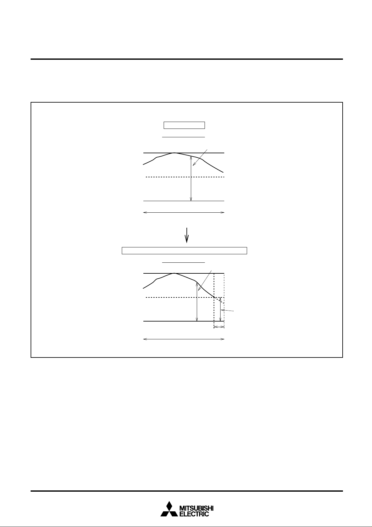
The M66332 performs entire pixel correction for 50% correction range as shown in Fig. 7.
White Correction
Analog signal input
V
WL
50%
V
BL
1 line
If correction range is exceeded (during white correction)
Analog signal input
V
WL
Correction is not possible if the white correction data exceeds
the 50% correction range as shown in Fig. 7. Therefore, be
sure to keep the input signal within the correction range.
White data
White data
5
2
-1
4
-1
2
0
5
2
-1
Fig. 7 Uniformity correction
50%
V
BL
1 line
4
-1
2
White data exceeding
correction range
0
Portion exceeding correction range
12
MITSUBISHI 〈DIGITAL ASSP〉
M66332FP
FACSIMILE IMAGE DATA PROCESSOR
• MTF compensation
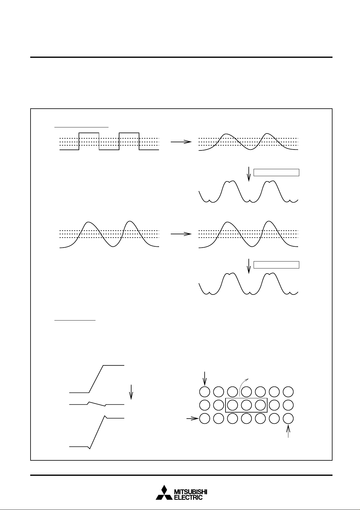
As shown in Fig. 8, characters and photos that have been
photoelectrically converted by the sensor unit are characterized by a drop in resolution. The MTF compensation per-
Photoelectric conversion
Source document (characters)
formed by the M66332 enhances the high frequency components with a Laplacian filter to maintain the resolution of the
image data and creates a perception of increased dynamic
range.
Photoelectric
conversion
Image signal
MTF compensation
Compensated data
Photoelectric
conversion
Source document (photo)
MTF compensation
Image signal
Compensated data
X’ = X + α ((X – A) + (X – B))
α = Primary scanning compensation coefficient, register 5 (MTF)
Secondary scanning direction
F
G
Primary scanning
direction
Window 3 × 1
AXB
MTF compensation
Fig. 8 MTF Compensation
F–G
Pixel
13
 Loading...