

MITSUBISHI 〈DIGITAL ASSP〉
MITSUBISHI 〈DIGITAL ASSP〉
DESCRIPTION
M66305A Toggle Line Buffer has two 5,120-bit line buffer
memories. It takes in serial data that arrives synchronously
with clock pulses and outputs it in serial at a rate of up to 10
Mbits per second synchronously with external clock pulses.
This buffer employs the double buffer system: While data is
being output, data on the next line can be written on the other
line buffer memory.
FEATURES
• 5,120 × 1bit serial input-serial output line buffer memories
• Data transmission at 10 megabits/second maximum
• Two line buffer memories can be alternated by external
toggle signal.
• Memory capacity can be doubled by cascade connection.
• Because of cascade input pin (CAS1), output potential after
completion of output can be set to either H or L.
• Low noise and high fan-out output (I
O = ±24mA guaranteed)
• Every input pin has built-in Schmidt trigger circuit.
• Read counter and write counter can be reset independently.
• RESET, T, CNTRST1 and CNTRST2 are equipped with
negative noise reduction circuit.
APPLICATION
Data buffer between industrial or home-use image data processing system and peripheral equipment
M66305AP/AFP
M66305AP/AFP
TOGGLE LINE BUFFER
TOGGLE LINE BUFFER
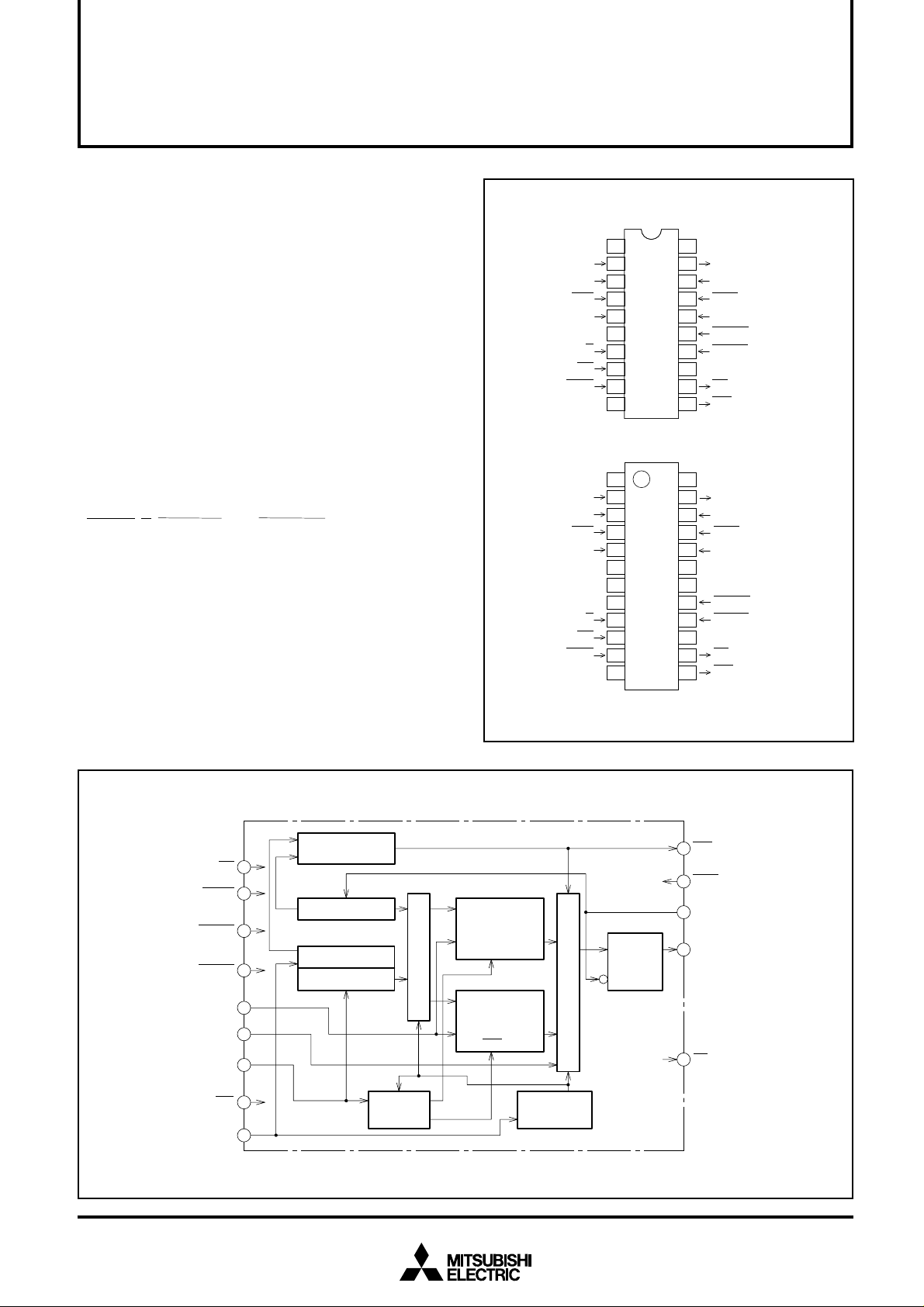
PIN CONFIGURATION (TOP VIEW)
GND
INPUT CLOCK
INPUT DATA
INPUT CLOCK ENABLE
CASCADE INPUT 1
TOGGLE SIGNAL INPUT
CHIP SELECT INPUT
RESET INPUT
SICLK
SIDATA
ICE
CAS1
GND
CS
RESET
GND
1
1
2
2
3
3
4
4
5
5
6
6
7
7
T
8
8
9
9
10
10
20
19
18
17
16
15
14
13
12
11
Outline 20P4
GND
INPUT CLOCK
INPUT DATA
INPUT CLOCK ENABLE
CASCADE INPUT 1
TOGGLE SIGNAL INPUT
CHIP SELECT INPUT
RESET INPUT
SICLK
SIDATA
ICE
CAS1
NC
NC
GND
CS
RESET
GND
1
1
2
2
3
3
4
4
5
5
6
6
7
7
8
8
9
9
T
10
10
11
11
12
12
24
24
23
23
22
22
21
21
M66305AFPM66305AP
20
20
19
19
18
18
17
17
16
16
15
15
14
14
13
13
V
CC
OUTPUT DATA
SODATA
SOCLK
OUTPUT CLOCK
OCE
OUTPUT CLOCK ENABLE
CAS2
CASCADE INPUT 2
CNTRST2
READ COUNTER RESET INPUT
CNTRST1
WRITE COUNTER RESET INPUT
V
CC
(5V)
BF
BUFFER FULL OUTPUT
INT
WRITE REQUEST OUTPUT
CC
V
OUTPUT DATA
SODATA
SOCLK
OUTPUT CLOCK
OCE
OUTPUT CLOCK ENABLE
CAS2
CASCADE INPUT 2
NC
NC
CNTRST2
READ COUNTER RESET INPUT
CNTRST1
WRITE COUNTER RESET INPUT
V
CC
(5V)
BF
BUFFER FULL OUTPUT
INT
WRITE REQUEST OUTPUT
BLOCK DIAGRAM
CHIP SELECT
INPUT
RESET INPUT
WRITE COUNTER
RESET INPUT
READ COUNTER
RESET INPUT
INPUT DATA
CASCADE INPUT 1
INPUT CLOCK
INPUT CLOCK
ENABLE
TOGGLE SIGNAL
INPUT
CS
RESET
CNTRST1
CNTRST2
SIDATA
CAS1
SICLK
ICE
T
Matching
detection circuit
Read counter
Write register
Write counter
and P.G.
Switch
AD
S-RAM
5120 bits
DI D0
WR
Address selector
A
D
S-RAM
5120 bits
DI D0
WR
Data selector
Toggle F/F
Outline 24P2W-A
INT
OCE
SOCLK
Data
buffer
SODATA
BF
NC: No Connection
WRITE REQUEST
OUTPUT
OUTPUT CLOCK
ENABLE
OUTPUT CLOCK
OUTPUT DATA
BUFFER FULL
OUTPUT
1

MITSUBISHI 〈DIGITAL ASSP〉
M66305AP/AFP
TOGGLE LINE BUFFER
FUNCTION
When the status of input clock enable (ICE) is “L”, input data
(SIDATA) is taken in (written) synchronously with input clock
(SICLK) rise edge. When output clock enable (OCE) is “L”,
output data (SODATA) is output (read) synchronously with
output clock (SOCLK) fall edge. The double buffer system
makes independent read and write operation possible.
When one-line write and one-line read are completed, toggle
eration is switched to read mode, and the line buffer which
has completed output is switched to write mode, enabling
next write and read operations.
To rewrite data during write operation, use write counter reset input (CNTRST1). To repeat output during output operation, use read counter reset (CNTRST2).
These operations are possible only when the status of chip
select (CS) is “L”.
signal (T) is required to be changed to “L”, With input of toggle
signal, the line buffer memory which has completed write op-
FUNCTION T ABLE
OutputInput
RES
L
H
H
H
H
H
H
H
H
H
H
H
Q0: No change
x : “H” or “L”
*1 : BF changes from “H” to “L” with rise of SICLK for write of 5120th bit.
*2 : With fall of SOCLK, data written before toggle signal input is output in order.
*3 : INT changes from “H” to “L” when the status of SOCLK rises after output of final bit of written before toggle signal inputs.
*4 : Outputs the first bit of written data (D
*5 : Output operation can be performed irrespective of CNTRST1.
*6 : SODATA changes to the first bit of written data (D0). Write operation can be performed irrespective of CNTRST2.
CS
X
H
L
L
L
L
L
L
L
L
L
L
ICE
X
X
H
L
H
L
L
H
L
H
X
X
SIC
X
X
X
X
L
X
L
X
X
X
OCE
X
X
H
H
L
L
X
X
X
X
L
H
SOC
X
X
X
X
L
L
X
X
L
X
0).
T
CR1
CR2
SOD
INT
BF
X
X
X
L
H
H
0
X
X
X
Q
H
H
H
Q
H
H
H
Q
H
H
H
H
H
H
H
H
H
H
H
H
H
H
H
H
H
H
0
Q
0
0
Q
0
0
Q
*2
*3
*2
*3
*4
H
*5
*5
*6
H
Initialization
0
Q
No internal change, no output change
0
Q
No internal change, no output change
*1
With rise of SICLK, data is written on line buffer memory.
0
Q
With fall of SOCLK, data is output.
*1
Write and read
With rise of T:
1)Line buffer memory in read mode is switched to write
H
mode and the other in write mode is switched to read
mode.
2)BF and INT are canceled.
With CNTRST1 input, internal write counter is reset,
H
enabling rewriting.
With CNTRST2 input, internal read counter is reset,
*6
enabling retrial of output.
Remarks
2
PIN DESCRIPTION
Pin
RESET
CS
ICE
SICLK
SIDATA
OCE
SOCLK
SODATA
T
BF
INT
CNTRST1
CNTRST2
CAS1
CAS2
NC
Name
Reset input
Chip select input
Input clock enable
Input clock
Input data
Output clock enable
Output clock
Output data
Toggle signal input
Buffer full output
Write request output
Write counter reset input
Read counter reset input
Cascade input 1
Cascade input 2
No Connection
MITSUBISHI 〈DIGITAL ASSP〉
M66305AP/AFP
TOGGLE LINE BUFFER
Functions
Initializes integrated circuit. (SODATA =“L”, BF =“H”, INT = “H”)
“L”: Chip select
“H”: Non-select (Inputs other than RESET have no effects on circuit inside.)
“L”: Input clock (SICLK) enable
“H”: Input clock (SICLK) disable
With rise of SICLK, SIDATA is written on line buffer memory.
“L”: Output clock (SOCLK) enable
“H”: Output clock (SOCLK) disable
With fall of SOCLK, SODATA is output. Because buffer is provided between memory and
output, each piece of data is propagated at a constant rate, irrespective of internal
memory read access time.
The line buffer memory in write mode is switched to read mode, and the other in read
mode is switched to write mode.
Output when SICLK rises for input of 5,120th bit, indicating no more writing is possible.
When BF is “L”, circuit inside is automatically set to “input disable”. BF is canceled with
rise of toggle signal (T) status.
Output when SOCLK rises after output of final bit of written data. When INT is “L”, circuit
inside is automatically set to “output disable”. INT is canceled with rise of toggle signal
(T) status.
Used to rewrite data during write operation when CS is “L”.
Used to undo data output halfway or to retry output when CS is “L”.
Output when SOCLK falls after output of final bit of written data. When cascade
connection is not used, be sure to connect this pin to VCC or GND.
Up to 2 cascade connections are possible. Connect the CA2 pin of master IC to VCC,
and the CA2 pin of slave IC to GND. Refer to APPLICATION EXAMPLE for details.
Non-connected pin provided only for M66305AFP. This pin can be used for wiring.
3

BASIC TIMING DIAGRAM
ICE
SICLK
MITSUBISHI 〈DIGITAL ASSP〉
M66305AP/AFP
TOGGLE LINE BUFFER
SIDATA
BF
T
OCE
SOCLK
SODATA
INT
* Circuit operates as shown in this timing chart in case one line length 5,120. If the line length is shorter than this, BF stays “H” status.
D0(B) D1(B) D2(B) D5118(B) D5119(B) D0(C)
D0(A) D1(A) D5118(A) D5119(A) CAS1 D0(B)
Start
Reset
OPERATION FLOWCHART
During the first cycle of operation after reset, write operation
is possible but read operation is impossible. Input toggle signal (T) after the one-line data is written.
During the second and following cycles, the previous written
data can be output or new data can be written in parallel. After one-line data is written and output is completed (INT output), input toggle signal (T).
Write operation
Write operation
Completion?
YES
Toggle signal
Output operation
Write
completion and INT
detection?
YES
Completion?
YES
END
NO
NO
NO
4

ABSOLUTE MAXIMUM RATINGS
Conditions
mounted
VCC
VI
VO
Pd
Tstg
Symbol
Parameter
Supply voltage
Input voltage
Output voltage
Power dissipation
Storage temperature
RECOMMENDED OPERATIONAL CONDITIONS (Ta = –10˚C ~ 70°C unless otherwise noted)
VCC
GND
VI
VO
Topr
Symbol
Supply voltage
Supply voltage
Input voltage
Output voltage
Operating ambient temperature
Parameter
Conditions
MITSUBISHI 〈DIGITAL ASSP〉
M66305AP/AFP
TOGGLE LINE BUFFER
–0.5 ~ +7.0
–0.5 ~ VCC + 0.5
–0.5 ~ VCC + 0.5
Min.
4.5
0.0
0.0
–10
Ratings
700
–65 ~ 150
Limits
Typ.
5.0
0.0
Max.
5.5
VCC
VCC
70
Unit
mW
Unit
V
V
V
°C
V
V
V
V
°C
ELECTRICAL CHARACTERISTICS (Ta = –10˚C ~ 70°C, VCC = 5V±10% and GND = 0V unless otherwise noted)
Symbol
VT+
VT–
VT+ - VT–
VOH
VOL
ICC
IIH
IIL
CI
The current flowing into the IC is positive current.
*Ta=25˚C
**Ta=70˚C
Positive threshold voltage
Negative threshold voltage
Hysteresis width
“H” output voltage
“L” output voltage
Quiescent supply current
“H” input current
“L” input current
Input capacitance
Parameter
Test conditions
All input
IOH=–24mA
IOL=+24mA
VI=VCC or GND
VI=5.5V
VI=0V
Min.
0.6
VCC – 0.8
Limits
Typ.
0.4
VCC–0.35*
VCC–0.4**
0.25*
0.30**
55*
45**
Max.
2.4
0.53
130
110**
+1.0
–1.0
10
Unit
V
V
V
V
V
mA
µA
µA
pF
5

MITSUBISHI 〈DIGITAL ASSP〉
M66305AP/AFP
TOGGLE LINE BUFFER
TIMING CONDITIONS (Ta = –10˚C ~ 70°C, VCC = 5V±10% and GND = 0V unless otherwise noted)
Symbol
tw±(SIC)
tw±(SOC)
tw(T)
tw(RES)
tw(CR1)
tw(CR2)
tsu(SID-SIC)
th(SIC-SID)
tsu(ICE-SIC)
th(SIC-ICE)
tsu(CS-SIC)
th(SIC-CS)
tsu(OCE-SOC)
th(SOC-OCE)
tsu(CS-SOC)
th(SOC-CS)
tsu(CS-T)
th(T-CS)
th(SIC-T)
trec(T-SIC)
th(SOC-T)
trec(T-SOC)
tsu(CS-CR1)
th(CR1-CS)
tsu(CS-CR2)
th(CR2-CS)
trec(R-SIC/SOC)
trec(CR1-SIC)
trec(CR2-SOC)
Note 2 To satisfy switching characteristic fmax = 10 MHz (frequency: 100ns), the condition shown below should be met: 100 ns ≤ (tW+) + (tW–)
Input clock pulse width (Note 2)
Output clock pulse width (Note 2)
Toggle signal input pulse width
Reset input pulse width
Write counter reset input pulse width
Read counter reset input pulse width
Input data setup time before input clock
Input data hold time after input clock
Input clock enable setup time before input clock
Input clock enable hold time after input clock
Chip select setup time before input clock
Chip select hold time after input clock
Output clock enable setup time before output clock
Output clock enable hold time after output clock
Chip select setup time before output clock
Chip select hold time after output clock
Chip select setup time before toggle signal input
Chip select hold time after toggle signal input
Toggle signal hold time after input clock
Input clock recovery time after toggle signal input
Toggle signal hold time after output clock
Output clock recovery time after toggle signal input
Chip select setup time before write counter reset
Chip select hold time after write counter reset
Chip select setup time before read counter reset
Chip select hold time after read counter reset
Input and output clock recovery time after reset
Input clock recovery time after write counter reset
Output clock recovery time after read counter reset
Parameter
30
43*
50
150
100
100
100
25
25
150
100
25
150
100
100
100
100
150
100
150
100
100
100
100
100
150
150
SWITCHING CHARACTERISTICS (Ta = –10˚C ~ 70°C, VCC = 5V±10% and GND = 0V)
Symbol
tc(SIC)
tc(SOC)
tPLH(SOC-SOD)
tPHL(SOC-SOD)
tPHL(SIC-BF)
tPHL(SOC-INT)
tPLH(T-BF)
tPLH(T-INT)
tPLH(R-BF)
tPLH(R-INT)
tPHL(CR1-BF)
tPLH(CR2-INT)
Note 3 AC test waveform ;
Input pulse level: 0V ~ 3V
Input pulse rise time: 6ns
Input clock cycle time
Output clock cycle time
Propagation time between input clock and output data
Propagation time between input clock and BF
Propagation time between output clock and INT
Propagation time between toggle signal input and BF
Propagation time between toggle signal input and INT
Propagation time between reset input and BF
Propagation time between reset input and INT
Propagation time between write counter reset and BF
Propagation time between read counter reset and INT
Parameter
Input pulse fall time: 6ns
Test conditions
100
100
CL=50pF
CL=150pF
CL=50pF
CL=150pF
CL=50pF
CL=150pF
CL=50pF
CL=150pF
CL=150pF
Test voltage ;
Input voltage: 1.3V
Output voltage: 1.3V
Limits
Typ.Min.
0
0
0
Limits
Typ.Min.
Max.
Max.
36
40
36
40
75
85
75
85
100
100
100
100
100
100
Unit
ns
ns
ns
ns
ns
ns
ns
ns
ns
ns
ns
ns
ns
ns
ns
ns
ns
ns
ns
ns
ns
ns
ns
ns
ns
ns
ns
ns
ns
*: Ta=25˚C
Unit
ns
ns
ns
ns
ns
ns
ns
ns
ns
ns
ns
ns
6

TIMING CHARTS
CS
ICE
SICLK
t
su(ICE-SIC)
t
su(CS-SIC)
t
su(SID-SIC)
t
c(SIC)
t
w-(SIC)
t
w+(SIC)
MITSUBISHI 〈DIGITAL ASSP〉
M66305AP/AFP
TOGGLE LINE BUFFER
t
h(SIC-ICE)
t
h(SIC-CS)
SIDATA
ICE
SICLK
CS
OCE
t
su(ICE-SIC)
t
h(SIC-SID)
(Note 4)
t
h(SIC-ICE)
Note 4. Timing to invalidate the clock.
SOCLK
SODATA
t
su(OCE-SOC)
t
su(CS-SOC)
t
c(SOC)
t
w+(SOC)
t
w-(SOC)
t
PLH(SOC-SOD)
t
PHL(SOC-SOD)
t
h(SOC-OCE)
t
h(SOC-CS)
7

OCE
SOCLK
SODATA
t
su(OCE-SOC)
t
h(SOC-OCE)
MITSUBISHI 〈DIGITAL ASSP〉
M66305AP/AFP
TOGGLE LINE BUFFER
CS
T
CS
CNTRST1
CS
t
su(CS-T)
t
su(CS-CR1)
t
w(T)
t
w(CR1)
t
h(TR1-CS)
t
h(T-CS)
CNTRST2
8
t
su(CS-CR2)
t
w(CR2)
t
h(TR2-CS)

T
SICLK
/SOCLK
BF
t
h(SIC-T)
t
h(SOC-T)
t
PHL(SIC-BF)
MITSUBISHI 〈DIGITAL ASSP〉
M66305AP/AFP
TOGGLE LINE BUFFER
t
rec(T-SIC)
t
rec(T-SOC)
t
PLH(T-BF)
INT
RESET
/CNTRST1
/CNTRST2
SICLK
/SOCLK
BF
INT
t
PHL(SOC-INT)
t
w(RES)
t
PLH(RES-BF)/(CR1-BF)
t
PLH(RES-INT)/(CR2-INT)
t
rec(RES-SIC)/(RES-SOC)
t
rec(CR1-SIC)
t
rec(CR2-SOC)
t
PLH(T-INT)
9

APPLICATION EXAMPLE
MITSUBISHI 〈DIGITAL ASSP〉
M66305AP/AFP
TOGGLE LINE BUFFER
SICLK
SIDATA
ICE
CS
RESET
GND
SICLK
SIDATA
ICE
CAS1
GND
T
T
CS
RESET
GND
GND
SICLK
SIDATA
ICE
CC
V
SODATA
SOCLK
OCE
CAS2
CNTRST2
CNTRST1
V
CC
BF
INT
CC
V
SODATA
SOCLK
OCE
SODATA
SOCLK
OCE
CC
V
CNTRST2
CNTRST1
(V
CC
CAS1
OR GND)
CAS1
GND
T
CS
RESET
GND
CAS2
CNTRST2
CNTRST1
V
CC
BF
INT
Note 5.
Output clock recovery time after toggle signal input [t
1) When one line length is 5,125 bits (5,120 +5) or less, t
is required to be 500 ns or more.
2) When one line length is 5,126 bits (5,120 +6) or more, t
is required to be 150 ns or more.
Note 6.
ICs used in this example connection:
M66305A: 2pcs.
M74HC32: 1pc.
GND
BF
INT
re(T-SOC):
rec(T-SOC)
rec(T-SOC)
10
 Loading...