

USB DEVICE CONTROLLER
D12
D13
INTRDWR
RST
CS
TEST2
Ver.1.0 Oct. 27, 2000
ADDRESS BUS
DATA BUS
READ STROBE
CHIP SELECT
RESET
DATA BUS
MITSUBISHI <DIGITAL ASSP>
M66290AGP/FP
DESCRIPTION
The M66290A is a general purpose USB (Universal Serial
Bus) device controller compatible with the USB
specification version 1.1 and corresponds to full speed
transfer. Built-in transceiver circuits meet all transfer type
which is defined in USB.
M66290A has FIFO of 3k Bytes for data transfer and can
set 6 endpoints (maximum).
Each endpoint can be set programmable of its transfer
condition, so can correspond to each device class transfer
system of USB.
FEATURES
· USB specification 1.1 compliant
· Built-in USB transceiver circuit
· Supports Full Speed (12 Mbps) transmission
· Supports all four USB transfer type :
· Control transfer
· Bulk transfer
· Isochronous transfer
· Interrupt transfer
· Built-in FIFO (3 KBytes) for Endpoint
· Up to 6 endpoint (EP0 to EP5) selectable
· Data transfer condition selectable for each
Endpoints (EP1 to EP5)
· Data transfer type
(Bulk, Isochronous and Interrupt)
· Transfer direction (IN/OUT)
· Buffer size of FIFO (maximum 1024 Bytes)
· Double (Toggle) buffer configuration
· Continuous transfer mode
(Buffering up to 1 KByteX2)
· Max packet size
· Supports 4 input clock frequencies
· Input clock : 6/12/24/48 MHz
· Built-in PLL which has an oscillation buffer
and outputs at 48 MHz
· Supports both 8-bit and 16-bit DMA transfers
· 16-bit CPU bus interface
· 3.3V single power source
· Built-in JTAG
APPLICATION
· Printer , Scanner , DSC , DVC
· PC camera , Multimedia speaker , Terminal adapter etc.
· Support all PC peripheral using Full Speed USB
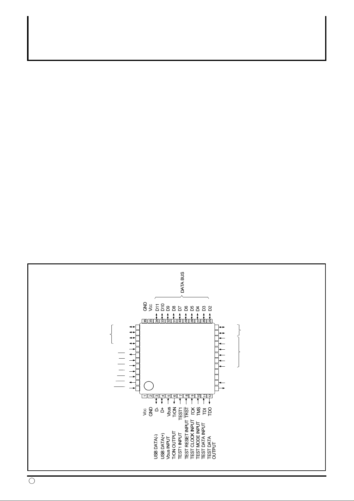
PIN CONFIGURATION
(TOP VIEW)
TEST2 INPUT
INTERRUPT
WRITE STROBE
DMA REQUEST
DMA ACKNOWLEDGE
Outline
M66290AGP:48P6Q-A(LQFP)
M66290AFP:48P6X-A(TQFP)
D14
D15
Dreq
Dack
24
37
38
39
40
41
42
43
44
45
46
47
48
M66290AGP
OR
M66290AFP
D1
23
D0
22
A6
21
A5
20
A4
19
A3
18
A2
17
A1
16
VCC
15
GND
14
13
OSCILLATOR INPUT
Xin
Xout
OSCILLATOR OUTPUT
c MITSUBISHI ELECTRIC CORPORATION
1
USB DEVICE CONTROLLER
XinCSRDWRINT
Dreq
GND
21536
Clock
Unit
A6 to 1
Register
(3KByte FIFO)
Dack
11635
4
3
Vbus
13
14
6
TrON
5
Xout
45
44434217222340
D15 to 0
47
48
41
7
RST
TEST2
TEST1
89101112
TRST
TCK
TMS
TDI
TDO
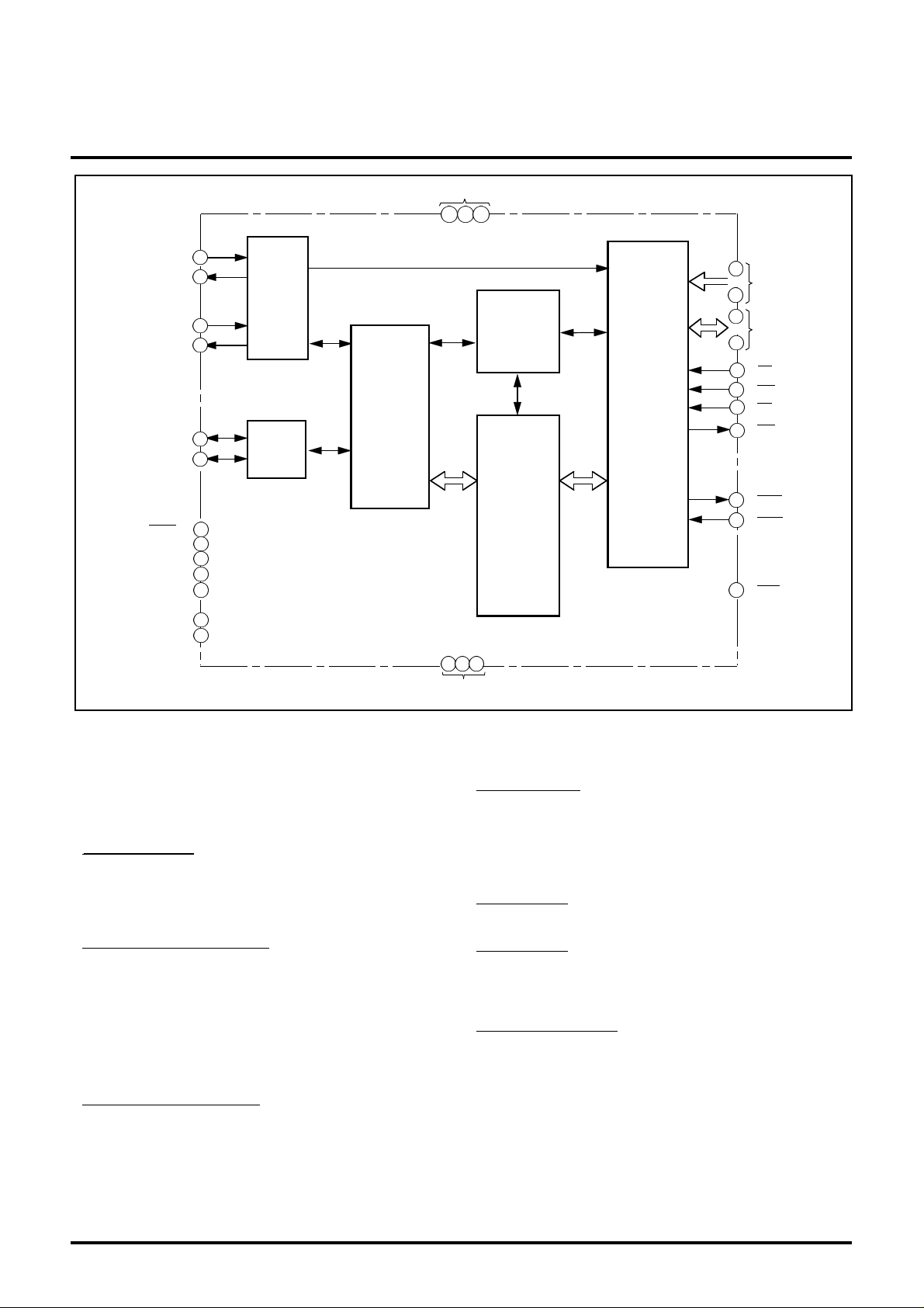
BLOCK DESCRIPTIONS
BLOCK DIAGRAM
Transceiver
Control
(Oscillator/
PLL)
MITSUBISHI <DIGITAL ASSP>
M66290AGP/FP
VCC
to
D+
USB
Peripheral
Circuit
Serial
Interface
Engine
USB
D-
Device
Control
Endpoint
Buffer
to
CPU
68
68
46
The M66290A contains USB transceiver, oscillation
circuit, PLL, serial interface engine, endpoint buffer,
device control unit, and CPU register.
USB Transceiver
USB Transceiver is consisted of differential driver
and differential receiver.
And is compatible with USB specification version 1.1
and corresponds to Full Speed Transfer mode.
Serial Interface Engine (SIE)
SIE handles protocol layer as follows.
Extract a USB 12MHz clock
Serial-Parallel data conversion
SYNC detection
NRZI encode and decode
Bit stuffing and destuffing
CRC generator and checker
Device Control Unit (DCU)
DCU controls the device state sequence, control
transfer sequence, and so on.
Endpoint Buffer
This is a FIFO buffer for transmit and receive
between endpoints.
Except for EP0 for control transfer, five endpoints
(EP1 to EP5) can be set.
CPU Register
This is an interface block with CPU.
Oscillator/PLL
This block oscillates the internal operation clock
source of 48MHz.
External clock of 6/12/24/48MHz can be input.
USB peripheral circuit
Detect the connection and the shutdown of USB
by the Vbus input.
Connect the Vbus of USB bus to or the 5V power
supply to Vbus input.
Connect the TrON output to D+ pull-up resistor of
1.5kohm. ON/OFF of the pull-up resistor is controlled
by the register.
2

USB DEVICE CONTROLLER
MITSUBISHI <DIGITAL ASSP>
OSCILLATO
OSCILLATO
-
ON/OFF control of the pull-up resistor is available.
Input/
PIN DESCRIPTIONS
M66290AGP/FP
Item Pin name
D15 to D0
CPU
interface
interface
interface
WR Input
INT Output
Dreq Output
DMA
D+
D-
USB
Vbus
TrON
DATA BUS
Input/
Data bus to access the register from the system
Output
ADDRESS BUS
Input A6 to A1
Address bus to access the register from the system
CHIP SELECT
Input CS
"L" level enables to communicate with M66290A
WRITE STROBE
Input data is written into the register by the positive edge
READ STROBE
Input RD
Register data can be read when "L" level
INTERRUPT
"L" level requests interrupt to system
DMA REQUEST
DMA transfer request to endpoint FIFO
DMA ACKNOWLEDGE
Input Dack
FIFO access by DMA transfer is available in "L" level
Input/
USB DATA(+)
Output
D+ of USB. Connect the external resistor serially.
USB DATA(-)
Input/
D- of USB. Connect the external resistor serially.
Output
Vbus INPUT (Built-in pull down resistor)
Input
Connect to the Vbus of USB bus or to the 5V power supply.
Connection or shutdown of the Vbus can be detected.
TrON OUTPUT
Output
Connect to the D+ pull-up resistor of 1.5kohm.
Function
Number of
16
6
1
1
1
1
1
1
1
1
1
1
JTAG
interface
Others
Input TRST
TMS Input
TCK
TDI
TDO
Input
Input
Output
Input RST
Input Xin
Output Xout
Input TEST1
Input TEST2
-
GND
TEST RESET INPUT (Built-in pull up resistor)
Reset input of JTAG. Even if the JTAG is not used, JTAG circuit must be
initialized. Input "L" level to initialize like the RST input.
TEST MODE INPUT (Built-in pull up resistor)
Mode set input to JTAG. If JTAG is not used, keep "H" level or open.
TEST CLOCK INPUT (Built-in pull down resistor)
Clock input to JTAG. If JTAG is not used, keep "L" level or open.
TEST DATA INPUT (Built-in pull up resistor)
Data input to JTAG. If JTAG is not used, keep "H" level or open.
TEST DATA OUTPUT
Data output from JTAG. If the JTAG is not used, keep open.
RESET
"L" level initializes the register or the counter of M66290A.
Generate an internal clock.
R INPUT
R OUTPUT
TEST1 INPUT (Built-in pull down resistor)
Input for the test. Keep "L" level or open.
TEST2 INPUT (Built-in pull down resistor)
Input for the test. Keep "L" level or open.
Power supply pin VCC
Ground
Input or output of internal clock oscillator. When use as a crystal oscillator, connect a
crystal between Xin and Xout.
If an external clock is used, input it to Xin, and Xout must be opened.
1
1
1
1
1
1
1
1
1
1
3
3
3

USB DEVICE CONTROLLER
USB DATA TRANSFER DESCRIPTIONS
Data receive
When M66290A received IN token packet again from host,
MITSUBISHI <DIGITAL ASSP>
M66290AGP/FP
M66290A is a USB device controller correspond to all
the four types of transfer (control, bulk, isochronous,
and interrupt transfer), which is compatible to USB
specification 1.1.
M66290A acts USB functions as below automatically.
(1) Bit stuffing/destuffing
(2) CRC generate/check
(3) NRZI encode/decode
(4) Packet handling
(5) USB address check
(6) Bus error handling
Therefore, when CPU transact the operations as
follows, USB transfer is realized.
(1) Response to the control transfer request
(2) Permission of store and transmission of the
transmit data into the endpoint buffer.
(Or read of the received data from the endpoint
buffer)
(3) Stall handling
(4) Suspend/resume handling
Below are the descriptions about the data transfer.
Data transmit
When the data of endpoint FIFO, which corresponds to
transmit request by IN token packet, is ready, M66290A
transmit the corresponded data packet to USB bus.
If the ACK packet come from the host for the transmitted
data packet, a transaction completed and the endpoint
FIFO becomes empty and urge CPU to write the next
transmit data by buffer ready interrupt.
If the transmit data, which correspond to transmit request
by IN token packet, is not exist in the endpoint FIFO,
M66290A transmit NAK packet to host when received
IN token packet from host and occurs interrupt and
request CPU to write transmit data.
M66290A transmits the data which is written.
If error is not occurred in that transfer, host transmit ACK
packet and if M66290A received it normally, a transaction
completed.
If USB protocol error is occurred in the data which is
transmitted via USB bus, host does not transmit ACK
packet, so M66290A watch and wait until receive IN token
packet, with keeping the data to be transmitted.
In data receive, there are differences of its function
between setup transaction and out transaction.
In setup transaction, when received device request
from host, 8Byte request is always stored into four
resistors.
When request data is received correctly,sends back
ACK packet to host and at the same time, occurs
interrupt to CPU and urge CPU to read request.
In out transaction, after M66290A received OUT
token packet, host transmits data packet.
If packet of maximum packet size or short packet
is stored into the endpoint FIFO of M66290A, and
moreover, error is not occurred in that transfer,
M66290A transmits ACK packet to host and informs
CPU that the data was received by occurring buffer
ready interrupt.
If USB protocol error is occurred in the host data
which received via USB bus, or if the endpoint FIFO
is full, M66290A does not transmit ACK packet to
host. Host knows that the error occurred because the
ACK packet does not come, and take a step such as
data resend.
4

USB DEVICE CONTROLLER
MITSUBISHI <DIGITAL ASSP>
-
0000h
0000h
R/W-0000h
0000h
R/W--------------
0000h
0000h
R/W
Interrupt Status Register2
1Ch-0000h
0000h
R/W
Interrupt Enable Register2
14h-0000h
0000h
-
0000h
0000h
-
0000h
0000h
Note 2
0000h
0000h
-
0000h
0000h
--0000h
--0000h
--0000h
--0000h
-
0000h
-
0008h
-
0000h
-
0000h
-
xxxx-0000h
-
0000h
-
0800h
-
xxxx-0000h
-
0800h
-
xxxx--
0000h
--0040h
--0000h
--0040h
--0000h
--0040h
--0000h
--0040h
--0000h
0000h
0000h
-
-
-
USB
0000h
0000h
0000h
-
S/W
0000h
0000h
0000h
H/W
R/W
R/W
R/W
R/W
R/W
R/WRRRRRR/W (note 2)
R/W
R/W
R/W (note 2)
R
R/W
R/W
R/W
R/W
R/W (note 2)
R/W
R/W
R/W (note 2)
R/W
R/W
R/W
R/W
R/W
R/W
R/W
R/W
R/W
R/W
EP5 Configuration Register0
EP4 Configuration Register1
EP4 Configuration Register0
EP3 Configuration Register1
EP3 Configuration Register0
EP2 Configuration Register1
EP2 Configuration Register0
EP1 Configuration Register1
EP1 Configuration Register0
Reserved
DMA_FIFO Data Register
DMA_FIFO Control Register
DMA_FIFO Selection Register
Reserved
CPU_FIFO Data Register
CPU_FIFO Control Register
CPU_FIFO Selection Register
Reserved
EP0 Continuous transmit Data Length
EP0_FIFO Data Register
EP0_FIFO Selection Register
Reserved
Auto-response Control Register
EP0 Packet Size Register
Control Transfer Control Register
Length Register
Index Register
Value Register
Request Register
Interrupt Status Register3
Interrupt Status Register1
Interrupt Status Register0
Interrupt Enable Register3
Interrupt Enable Register1
Interrupt Enable Register0
Reserved
IsochronousStatus Register
USB_Address Register
Reserved
Sequence Bit Clear Register
Remote Wake-up Register
USB Operation Enable Register
4Eh to 5Eh
70h
6Eh
6Ch
6Ah
68h
66h
64h
62h
60h
4Ch
4Ah
48h
46h
44h
42h
40h
38h to 3Eh
36h
34h
30h
2Eh
2Ch
2Ah
28h
26h
24h
22h
20h
1Eh
1Ah
18h
16h
12h
10h
0Ch to 0Eh
0Ah
08h
06h
04h
02h
00h
CONTROL REGISTER TABLE
M66290AGP/FP
Below is the table of registers of M66290A.
Bit width of all register is 16bits.
In reset item, "H/W" shows the reset status
by external RST input, "S/W" shows reset
status by USBE register, and "USB"
Address Name R/W
shows the reset status by receiving USB reset.
" - " shows that the previous status is kept.
Write into reserved address is inhibited.
32h
note 1 : Detail description is mentioned later.
note 2 : Some are read only.
EP0_FIFO Control Register
R/W (note 2)
5
-0800h
USB DEVICE CONTROLLER
Functional and register descriptions
We explain about Function and register constitution of
M66290A dividing into four items as follows.
by self oscillation.
n USB reset (when more than 2.5us of SE0 state
firmware to manage incorrect transfer in case of transfer
from CPU as follows, USB_Address register (USB_Addr),
process, that is, enables clock input by XCKE, wait
until oscillation stabilized (less than 1ms), and start
wakeup signal and can cancel suspended state to receive
(1) System control
(2) Interrupts
(3) Control transfer/enumeration
(4) Endpoints and FIFO control
(1) System control
CLOCK
Clock of 48MHz is needed for internal operations
of M66290A.
Built in PLL enables to input external clock of 6/12/
24/48MHz. Selection of it is realized by the XTAL
of "USB Operation Enable Register".
When use external clock of 48MHz, PLL is not
needed, so set to PLL operation disable.
Built in oscillation circuit enables to supply clock
To set the "USB Operation Enable Register", it can
be set the device to standby state. Oscillation is
halted (clock input halted) by XCKE, PLL operation
is halted by PLLC, and clock supply to USB block
is halted by SCKE.
To prevent unstable behavior by unstable clock,
clock supply to USB block must be obeyed the
until oscillation stabilized, start PLL by PLLC, wait
clock supply to USB block by SCKE.
RESET
S/W reset by the register set (USBE), different from
the hardware reset, keeps the value of register of
USB operation enable register, FIFO relational
register, control transfer relational register,endpoint
setting register, and so on.
And i
is continued on D+, D- terminal), the value of register
is kept except for "Interrupt Status Register 0" and
"USB_Address Register"
As to details of reset state, see each item of register.
D+ pull-up resistor control function
To set the register, external TrON output is controlled
and can control the ON/OFF of pull-up resistor
(1.5kohm) on USB D+ line.
Remote wakeup function
When device is in suspended state, outputs remote
resume from USB.
Remote wakeup function is only effective in Suspended
state in which device state shifts from Configured state,
so don't use to other device state.
MITSUBISHI <DIGITAL ASSP>
M66290AGP/FP
And when use this function, device state shifts to Address
state after outputs remote wakeup signal, so it is needed
to set up again the device state to Configured state.
Change of set up of device state can be done in S/W
control mode.
Remote wakeup signal is a signal to set USB bus to idle
state after output K-state of 10ms length.
If this remote wakeup function is set up immediately after
detected suspend, USB bus idle state is kept for 2ms and
then shifts to K state output. (Because USB bus idle state
must be kept for 5ms minimum until transmit of remote
wakeup signal, on the other hand after detect suspend,
USB idle state is continued for 3ms)
Sequence toggle bit clear function
In each endpoint of EP0 to EP5, data PID can be reset
independently and also can appoint PID of DATA0.
By this function, management of sequence toggle bit
in transfer after reset PID, is done by H/W automatically.
Error information in isochronous transfer
In isochronous transfer there is not retry function of
transmit/receive, because the handshake from receiver
to transmitter is not returned not to disturb the time
equivalent data transfer.
M66290A has enough information function which enables
error occurred in isochronous transfer.
Information which M66290A can inform is, over run
error, under run error, received data error (CRC error,
bit stuffing error), and frame number.
Software control mode
In software control mode, it is available to set up (write)
device state register (DVSQ), control transfer stage
register (CTSQ).
Normally, use this mode with OFF.
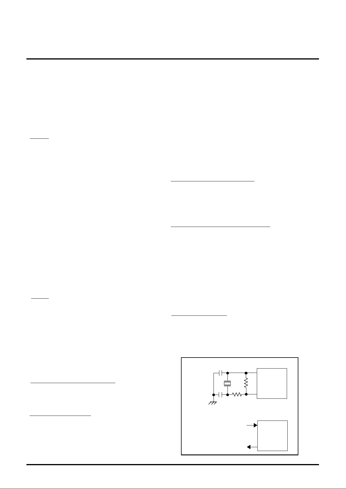
(1) In case of crystal oscillation
Place the parts as near the terminal as possible
(2) In case of external clock input
Figure 1. Xin and Xout connections
C1
XTAL
Rd
C2
clock input
open
Rf
Xin
M66290A
Xout
Xin
M66290A
Xout
6

USB DEVICE CONTROLLER
MITSUBISHI <DIGITAL ASSP>
USBPC
(1-2) Remote Wake-up Register
(Address : 02h)
(1-1) USB Operation Enable Register (Address : 00h)
M66290AGP/FP
D0D1D2D3D4D5D6D7D8D9D10D11D12D15 D13D14
SCKEPLLCXCKE USBE
Tr_on[1:0]XTAL[1:0]
SCTR
Bit
14
13, 12
11
10
9, 8
Bit
Name
XCKE15 Oscillator enable
SCKE
USBPC
Tr_on
[1:0]
Name Function W/R
PLL controlPLLC
Crystal selectXTAL[1:0]
Internal clock
enable
USB transceiver
power control
Tr_on output
control
0 : Oscillator disable (clock input disable)
1 : Oscillator enable (clock input enable)
0 : PLL disable
1 : PLL enable
When use external clock of 48MHz, set to PLL disable.
00 : 1/1 division (external 48MHz input)
10 : 1/2 division (external 24MHz input)
01 : 1/4 division (external 12MHz input)
11 : 1/8 division (external 6MHz input)
0 : Internal clock (sck) disable
1 : Internal clock (sck) enable
0 : USB transceiver disable
1 : USB transceiver enable
In suspend state, resume signal can be received even if USB
transceiver disabled.
X0 : TrON port ="Hi-Z"
01 : TrON port ="L"
11 : TrON port ="H"
This fields selects TrON output state, and it is effective when
external Vbus input is "H" level (5V). If external Vbus input is "L",
these bits can be set but TrON output does not operate.
Reset
USBS/WH/W
--0W/R
--0W/R
--00W/R
--0W/R
--0W/R
--00W/R
Reserved
7 to 2
0
Bit
Reserved
15 to 1
0 Remote wake-upWKUP
SCTR1
USBE
Bit
Name
Software control
mode
USB module
enable
Name
Write/Read "0"
0 : Normal Operation
1 : Software Control Mode Operation
0 : USB module disable (S/W Reset)
1 : USB module enable
Function W/R
Write/Read "0"
When CPU write "1" to WKUP for remote wake-up, M66290A outputs
K-State for 10ms, and return to Bus Idle-State.
(Remote wake-up signal)
This bit returns to "0" automatically after suspend is canceled.
If "1" is written into this bit after detected suspend, bus idle state is kept
for 2ms and after then shifts to K state output.
--0W/R
--0W/R
D0D1D2D3D4D5D6D7D8D9D10D11D12D15 D13D14
WKUP
Reset
USBS/WH/W
-00W/R
7

USB DEVICE CONTROLLER
MITSUBISHI <DIGITAL ASSP>
Sequence toggle bit
(1-3) Sequence Bit Clear Register (Address : 04h)
(1-4)USB Address Register (Address
:
08h)
M66290AGP/FP
D0D1D2D3D4D5D6D7D8D9D10D11D12D15 D13D14
SQCLR[5:0]
Bit Name Function W/R
15 to 6
5 to 0
Bit
15 to 7
Bit
Name
Reserved
SQCLR
[5:0]
Bit
Name
Reserved
Write/Read "0"
When write "1" into the bit which is correspond to the number
of endpoint, sequence toggle bit of that endpoint is cleared
and appoint the DATA0 by the data PID of next transmission.
Write "1" into the bit after set the response PID of the endpoint, which
clears sequence toggle bit, to NAK("00") .
clear
Name Function W/R
Transfers After the transfer appointed, sequence toggle bit is controlled
by H/W.
In USB reset, Sequence toggle bit of each endpoint is not cleared.
If "0" is written into this bit, flag is not changed.
Read data of this bit is always "0".
USB_Addr[6:0]
Write/Read "0"
Reset
USBS/WH/W
-00h00hW/R
D0D1D2D3D4D5D6D7D8D9D10D11D12D15 D13D14
Reset
USBS/WH/W
6 to 0 USB_Address
USB_
Addr
[6:0]
register
USB address which is assigned by host is stored.
After stored the address, transaction is done only to the token packet
which is transmitted to this address.
(If S/W control mode is set, write operation is available)
8
00h00h00hR

USB DEVICE CONTROLLER
MITSUBISHI <DIGITAL ASSP>
(1-5) Isochronous Status Register
(
Address
:
0Ah
)
FMODCRCEOVRN FRNM[10:0]
M66290AGP/FP
D0D1D2D3D4D5D6D7D8D9D10D11D12D15 D13D14
Bit
Name
OVRN15 Over run error
14
FunctionNameBit
In isochronous transfers (OUT/IN), when over-run or under-run is
occurred to the endpoint buffer, this flag is set at the timing of the
receive end of the OUT/IN token packet.
Over run is occurred when delayed to read the received data from
the endpoint buffer, and means that could not received. Over run is
occurred when the direction of transmission is OUT.
Also the received data has CRC or bit stuffing error, this flag is set.
Under run is occurred when delayed to write the transmit data into the
endpoint buffer, and means that could not transmitted. Under-run is
occurred when the direction of transmission is IN.
When a state above is occurred, endpoint buffer notready interrupt is
occurred.
When "0" is written, status flag is cleared.
When "1" is written, flag is not changed.
In isochronous transfers(OUT), if the received data has CRC or
bit stuffing error, this flag is set at the timing of the end of transaction.
When a state above is occurred, endpoint buffer notready interrupt is
Receive data errorCRCE
occurred.
W/R
Reset
USBS/WH/W
-00W/R
-00W/R
13 to 12
Reserved
FMOD11
FRNM
[10:0]
Frame number
mode
Frame number10 to 0
When "0" is written, status flag is cleared.
When "1" is written, flag is not changed.
Write/Read "0"
Select the renewal timing of the flame number to be stored
to FRNM[10:0].
0 : Renew the flame number when SOF is received .
1 : In isochronous transfer, renew the flame number at the
timing of the end of transaction.
Stores the flame number.
The timing to renew the stored flame number is selectable by set
FMOD.
-00W/R
-000h000hR
9

USB DEVICE CONTROLLER
(2) Interrupts
There are eight factors of interrupt to CPU.
If disable is set, interrupt is not occurred but interrupt
When buffer of each endpoint became ready
If the internal clock(sck) is halted, status flag can not
Summary of interrupts
When interrupt occurred, the factor can be known to
refer to "Interrupt Status Register 0" and "Interrupt
Status Register 1".
These interrupts can be set of its enable/disable
independently to set "Interrupt Enable Register 0"
and "Interrupt Enable Register 1".
status flag is set.
Each factor of interrupt is shown in the table below,
and also describes below the interrupt conditions and
how to deal with the interrupt.
MITSUBISHI <DIGITAL ASSP>
M66290AGP/FP
Resume detect interrupt (RESM)
If device state is in suspended state and resume interrupt
enable flag is set, interrupt occurs when USB bus state
is changed ("J" to "K" or "SE0").
This interrupt can be occurred even if the internal
clock(sck) is halted. To clear the status flag, set the
internal clock(sck) in operation and then write "0". If the
internal clock(sck) is halted, status flag can not be
cleared.
SOF detect interrupt (SOFR)
Interrupt occurs when detect SOF.
Vbus (connect/shut down) interrupt (VBUS)
Interrupt occurs when Vbus input state is changed
(both "L" to "H" and "H" to "L").
To know Vbus input state, confirm the Vbus bit of
interrupt status register 0. Confirmation of Vbus bit
must be done after enabled internal clock operation.
This interrupt can be occurred even if the internal
clock(sck) is halted. To clear the status flag, enables
the internal clock(sck) in operation and then write "0".
be cleared.
This interrupt is useful to detect connect/shut-down of
USB for prepareration/close of USB transfers.
Status bit Name
VBUS
RESM Resume detect interrupt
Vbus interrupt
(connec/shut-down detect)
Change of the Vbus input
(both "L" to "H" and "H" to "L")
Resume signal received in suspended
Device state transition interrupt (DVST)
M66290A manages the device state by H/W.
It manages Powered, Default, Address, Configured, and
Suspended state. Device state can be known to refer to
"Interrupt Status Register 0".
As to device state shift, see the item of "Device state
shift" in "(3) Control transfer/emulation" in the latter part.
Device state transition interrupt occurs when device state
shifted. The number of factors is four, that is, USB bus
reset detect, suspend detect, execution of "Set Address",
and execution of "Set Configuration".
USB reset is detected when SE0 state over 2.5us is
continued on D+, D- terminal.
Suspend is detected when idle state over 3ms is
continued on D+, D- terminal.
Abstract of interrupt factor
Relational status bit
Vbus
SOFR SOF detect interrupt Received SOF
DVST
CTRT
BEMP
INTN
INTR
device state transition
interrupt
Control transfer
stage transition interrupt
Endpoint buffer
empty/size-over interrupt
Endpoint buffer not ready
interrupt
Endpoint buffer ready
interrupt
In each endpoint, when data transmit of all buffer
is ended and buffer is empty, or in OUT transfer,
received packet which exceeds max packet size.
When buffer is in not ready state (SIE cannot read
and write) to IN/OUT token of each endpoint.
(read enable/write enable)
Shift of device state DVSQ[2:0]
Stage shift of control transfer
10
CTSQ[2:0]
EPB_EMP_OVR[5:0]
EPB_NRDY[5:0]
EPB_RDY[5:0]

USB DEVICE CONTROLLER
MITSUBISHI <DIGITAL ASSP>
For example by using this interrupt, when USB bus reset
Control transfer stage transition interrupt (CTRT)
If the transfer direction is set to OUT, interrupt occurs
M66290AGP/FP
Each of "Set Address" and "Set Configuration" execution
detects the device state shift by analyzing the device
request in control transfer.
Each of these four factors can be set of its interrupt to
enable or disable by setting the corresponded bit of
interrupt enable register 0.
is detected, a step to USB bus is available and when
suspend is detected, a step to shift device to low power
consumption.
M66290A manages the sequence of control transfer
by H/W.
Each stage of control transfer, such as setup stage,
data stage, and status stage can be known to refer to
the "Interrupt Status Register 0".
Control transfer stage transition interrupt is occurred
when the control transfer stage is shifted.
There are five factors, that is, setup stage end,
control write transfer stage shift, control read transfer
stage shift, control transfer end, and control transfer
sequence error.
Except for setup stage, Each of these four factors can
be set of its interrupt to enable or disable by setting the
corresponded bit of interrupt enable register 0.
As to control transfer sequence error which can be
recognized by H/W, refer to "Control transfer stage
shift" in the item of "(3) Control transfer/enumeration"
in the latter part.
Endpoint buffer empty/size-over interrupt (BEMP)
Interrupt factor is different by transfer direction of
endpoint.
1. In case of transfer direction is IN
In each endpoint, interrupt occurs when transmission
ended of all data which is stored in the buffer.
By this interrupt, when endpoint is set to double buffer,
end of data transmission of all data of the buffer can
be known.
And also can know the end of data transmission of
control read transfer in endpoint 0 (EP0).
Endpoint buffer not ready interrupt (INTN)
When the buffer is in not ready state to IN/OUT token
of each endpoint, interrupt occurs at the timing of token
packet receive end.
By refer to EPB_NRDY[5:0] of interrupt status register 1,
it can be known which endpoint occurred the interrupt.
If endpoint is set to isochronous transfer, when over-run/
under-run error is occurred, interrupt occurs at the timing
of token packet receive end.
And if it is set to isochronous (OUT), if received data
has
error such as CRC error, interrupt occurs at the timing of
transaction end.
The variety of error in isochronous transfer is known to
refer "Isochronous Status Register".
Endpoint buffer ready interrupt (INTR)
Interrupt occurs when the buffer of each endpoint
became ready (read/write is available).
It can be known which endpoint occurred the interrupt
to refer EPB_RDY[5:0] of interrupt status register 1.
According to the endpoint and its access mode, the
factor of interrupt is different as follows.
1. In case of EP0
Interrupt occurs when receive (OUT) buffer of endpoint
0 became ready.
If it is set to control write continuous receive mode,
when continuous receive of 255 bytes ended or when
received short packet, interrupt occurs.
Interrupt is not occurred even if the transmit buffer
became ready.
2. In case of EP1 to EP5, when CPU access
Interrupt occurs when the buffer of each endpoint
became ready.
3. In case of EP1 to EP5, when DMA access
when received short data packet and then ended DMA
transfer.
Interrupt is not occurred if the transfer direction is set
to IN.
2. In case of transfer direction is OUT
In each endpoint, interrupt occurs in data packet
receive when received packet which exceeds the
maximum packet size.
By refer to EPB_EMP_OVR[5:0] of interrupt status
register, it can be known which endpoint occurred the
interrupt.
11

USB DEVICE CONTROLLER
Figure 2. shows the examples of interrupt output timing
(1) Endpoint buffer ready interrupt (ex.OUT transaction)
OUT token packet Data packet Hand shake packet (ACK)
MITSUBISHI <DIGITAL ASSP>
M66290AGP/FP
USB
SYNC
PID
Addr
Endp CRC
EOP
SYNC
INT output
(2) Endpoint buffer not ready interrupt (ex.OUT transaction)
OUT token packet Data packet Hand shake packet (NAK)
USB
SYNC
PID
Addr
Endp CRC
EOP
SYNC
INT output
(3) Endpoint buffer not ready interrupt (ex.IN transaction)
IN token packet Hand shake packet (NAK)
USB
SYNC
PID
Addr
Endp CRC
EOP
SYNC
PID
DATA
CRC
EOP
SYNC
Buffer becomes ready (read enable)
and interrupt occurs
PID
DATA
CRC
EOP
SYNC
Buffer is in not ready (receive disable)
and interrupt occurs
PID EOP
PID EOP
PID EOP
INT output
Figure 2. Examples of interrupt output timing
Buffer is in not ready (transmit disable)
and interrupt occurs
12

USB DEVICE CONTROLLER
MITSUBISHI <DIGITAL ASSP>
BEMPE
(2-1) Interrupt Enable Register 0 (Address
:
10h)USB DEVICE CONTROLLER
M66290AGP/FP
D0D1D2D3D4D5D6D7D8D9D10D11D12D15 D13D14
WDST
RDSTINTNECTRE SERRCMPLSUSPSCFGSADRURSTINTREDVSESOFERSMEVBSE
Bit
14
13
12
11
10
Bit
Name
VBSE15
RSME
SOFE
DVSE
CTRE
BEMPE
INTNE
9
8
INTRE
Name
Vbus interrupt
enable
Resume interrupt
enable
SOF interrupt
enable
Device state
interrupt enable
Control transfer
interrupt enable
Endpoint5-0 buffer
empty/size error
interrupt enable
Endpoint5-0 buffer
not ready
interrupt enable
Endpoint5-0 buffer
ready
interrupt enable
Function W/R
0 : Disable
1 : Enable
0 : Disable
1 : Enable
0 : Disable
1 : Enable
0 : Disable
1 : Enable
0 : Disable
1 : Enable
0 : Disable
1 : Enable
0 : Disable
1 : Enable
0 : Disable
1 : Enable
Reset
USBS/WH/W
-00W/R
-00W/R
-00W/R
-00W/R
-00W/R
-00W/R
-00W/R
-00W/R
7
URST
6
SADR
5
SCFG
4
SUSP
WDST
3
2
RDST
1
CMPL
0
SERR
Set Address
execute
Set Configration
execute
Suspend
detect
Control write
transfer status
stage
Control read
transfer status
stage
Control transfer
complete
Control transfer
sequence error
If this bit is "1", then the DVST flag is set when detected USB reset.USB reset detect
If this bit is "1", then the DVST flag is set after executed SetAddress.
If this bit is "1", then the DVST flag is set after executed SetConfigration.
If this bit is "1", then the DVST flag is set when detected suspend.
If this bit is "1", then the CTRT flag is set when shifted to status stage
in control write transfer.
If this bit is "1", then the CTRT flag is set when shifted to status stage
in control read transfer.
If this bit is "1", then the CTRT flag is set when control transfer
completed (when the status stage completed normally).
If this bit is "1" then the CTRT flag is set when error
occurred in the sequence of control transfer.
-00W/R
-00W/R
-00W/R
-00W/R
-00W/R
-00W/R
-00W/R
-00W/R
13
MITSUBISHI <DIGITAL ASSP>
(2-2) Interrupt Enable Register
1(
Address
:
12h
)
(2-4) Interrupt Enable Register 3
(
Address
:
16h
)
(2-3) Interrupt Enable Register
2 (
Address
:
14h
)
M66290AGP/FP
D0D1D2D3D4D5D6D7D8D9D10D11D12D15 D13D14
EPB_RE[5:0]
Bit
5 to 0
Bit
5 to 0
Bit
Name
Reserved15 to 6
EPB_RE
[5:0]
Bit
Name
Reserved15 to 6
EPB_NRE
[5:0]
Name Function W/R
Write/Read "0"
Endpoint5-0 buffer
ready
interrupt enable
Name Function W/R
Endpoint5-0 buffer
not ready
interrupt enable
0 : Disable
1 : Enable
The number of endpoint is correspond to each bit one by one.
Write/Read "0"
0 : Disable
1 : Enable
The number of endpoint is correspond to each bit one by one.
Reset
USBS/WH/W
-00h00hW/R
D0D1D2D3D4D5D6D7D8D9D10D11D12D15 D13D14
EPB_NRE[5:0]
Reset
USBS/WH/W
-00h00hW/R
Name
Reserved15 to 6
EPB_
EMPE
Bit
[5:0]
Endpoint5-0 buffer
empty/size error
interrupt enable
Bit
5 to 0
EPB_EMPE[5:0]
Name Function W/R
Write/Read "0"
0 : Disable
1 : Enable
The number of endpoint is correspond to each bit one by one.
14
D0D1D2D3D4D5D6D7D8D9D10D11D12D15 D13D14
Reset
USBS/WH/W
-00h00hW/R

USB DEVICE CONTROLLER
MITSUBISHI <DIGITAL ASSP>
(2-5) Interrupt Status Register 0
(
Address
: 18h)
M66290AGP/FP
D0D1D2D3D4D5D6D7D8D9D10D11D12D15 D13D14
BEMP INTN VALIDDVSQ[2:0] CTSQ[2:0]CTRT VbusINTRDVSTSOFRRESMVBUS
Bit
Name
This bit changes to "1" when Vbus input changed both "0" to "1" and
"1" to "0".
As to the Vbus input state, confirm to see the bit of Vbus input port.
Vbus interrupt
14
RESM
SOFR
13
12
DVST
Resume detect
interrupt
SOF detect
interrupt
Device state
transition interrupt
This bit is set even if the internal clock (sck) is in halt state.
If "0" is written after enabled internal clock as operation, status flag is
cleared. But if internal clock is in halt state, flag is not cleared.
If "1" is written, flag is not changed.
This bit changes to "1" when USB bus state changed("J" to "K" or "SE0")
under the condition that resume interrupt enable flag is set.
This bit is set even if the internal clock (sck) is in halt state.
If "0" is written after enabled internal clock as operation, status flag is
cleared. But if internal clock is in halt state, flag is not cleared.
If "1" is written, flag is not changed.
This bit changes to "1" when detected SOF.
If "0" is written, status flag is cleared.
If "1" is written, flag is not changed.
This bit changes to "1" when device state shifted.
There are four factors, that is, USB reset detect, suspend detect,
"Set Address" execution, and "Set Configuration" execution.
These four factors can be masked by the corresponded bit of
"Interrupt Enable Register0" .
If "0" is written, status flag is cleared.
If "1" is written, flag is not changed.
FunctionNameBit
W/R
Reset
USBS/WH/W
-00W/RVBUS15
-00W/R
-00W/R
100W/R
Control transfer
11
CTRT
BEMP10
stage transition
Endpoint5-0 buffer
empty/size error
interrupt
interrupt
This bit changes to "1" when the stage of control transfer is shifted.
There are five factors, that is, setup stage end, control write transfer
status stage shift, control read transfer status stage shift, control transfer
end, and control transfer sequence error.
Four factors, except for setup stage end, can be masked by the
corresponded bit of the "Interrupt Enable Register0".
If "0" is written, status flag is cleared.
If "1" is written, flag is not changed.
The factor is different by the direction of the transfer of each endpoint.
In each endpoint, this bit changes to "1" when the transmission of all
stored data is completed (direction:IN) and when received the packet
which is exceeded to maximum packet size (direction:OUT).
The endpoint which occurs the interrupt can be checked to see the
EPB_EMP_OVR[5:0].
This flag is cleared to clear the status flag of EPB_EMP_OVR[5:0].
15
-00W/R
-00R

USB DEVICE CONTROLLER
MITSUBISHI <DIGITAL ASSP>
M66290AGP/FP
Bit
Bit
Name
INTN9
INTR8
7
Vbus
Name Function
This bit changes to "1" at the timing of token packet receive end when
buffer respond NAK, of its not ready state, to IN/OUT token of each
Endpoint5-0 buffer
not ready
interrupt enable
Endpoint5-0 buffer
ready
interrupt enable
Vbus input port
endpoint.
The endpoint which occurred the interrupt is checked to see
EPB_NRDY[5:0].
This flag is cleared to clear the status flag of EPB_NRDY[5:0].
This bit changes to "1" when the buffer of each endpoint
became ready (read/write enable).
The endpoint which occurred the interrupt is checked to see
EPB_RDY[5:0].
This flag is cleared to clear the status flag of
EPB_RDY[5:0].
Input data from external Vbus is stored.
0: Vbus input port is "L"
1: Vbus input port is "H"
External Vbus input data is latched by the positive edge of internal clock.
Refer to this bit after enabled internal clock operation.
W/R
Reset
USBS/WH/W
-00R
-00R
Ext.Ext.Ext.R
6-4
3
2-0
DVSQ
[2:0]
VALID
CTSQ
[2:0]
Device state
Setup packet
detect
Control transfer
Stage
000: Powered State
001: Default State
010: Address State
011: Configured State
1xx: Suspended State
Device state can be known.
As to the device state shift, refer to Fig.5 in the later part.
When detect USB reset, this becomes 001: Default state automatically.
When detect suspend, this becomes 1xx: Suspended state automatically.
Whatever the automatic response mode is, this becomes 010: Address
state after executed Set_Address request, and becomes 011: Configured
state after executed Set_Configuration request.
(Write operation is available when S/W control mode is set)
This bit changes to "1" when received setup packet.
This flag does not the factor of interrupt.
When "0" is written, status flag is cleared .
When "1" is written, flag is not changed .
000 : Idle or Setup stage
001 : Control read transfer data stage
010 : Control read transfer status stage
011 : Control write transfer data stage
100 : Control write transfer status stage
101 : Control write no data transfer status stage
110 : Control transfer sequence error
111 : Not assigned
Can be seen the stage of control transfer.
As to the stage shift of control transfer, refer to Fig.5 in the later part.
(Write operation is available when S/W control mode is set)
R
W/R
R
001000000
-00
-000000
16

USB DEVICE CONTROLLER
MITSUBISHI <DIGITAL ASSP>
(2-6) Interrupt Status Register 1
(Address : 1Ah)
M66290AGP/FP
D0D1D2D3D4D5D6D7D8D9D10D11D12D15 D13D14
EPB_RDY[5:0]
Bit
15 to 6
5 to 0
Bit
Name
Reserved
EPB_RDY
[5:0]
Endpoint5-0 buffer
ready
interrupt
FunctionName
Write/Read "0"
When buffer becomes ready (read/write enabled) to each endpoint,
the bit which corresponds to the number of endpoint changes to "1".
The factor of the interrupt is different by the transfer condition of each
endpoint.
1. As to EP0
This bit changes to "1" when receive buffer(OUT) became ready
(read enabled) in control write transfer.
If it is set to control write continuous receive mode or completed
receiving of the data of 255Bytes or received short data packet,
this bit changes to "1".
This bit is not changed even if the transmission buffer(IN) became
ready (write enabled) in control read transfer.
The ready state of the transmission buffer(IN) can be known by the
buffer empty interrupt.
2. As to EP1 to EP5, when CPU access
This bit changes to "1" when each buffer of each endpoint became
ready(read/write enabled).
This bit also changes to "1" when set the direction of the transfer to IN
in initialization.
3. As to EP1 to EP5, when DAM access
If the direction of the transfer is set to OUT, this bit changes to "1"
when received short data packet and then completed DMA transfer
of received data.
In this case, clear is only available to write the BCLR command.
This bit is not changed if the direction of transfer is set to IN.
W/R
R -00h00h
Reset
USBS/WH/W
Clearance of this flag is different by the transfer direction of endpoint.
1. If the transfer direction is OUT
After set the number of the object endpoint to the "FIFO Selection
Register", write BCLR command or read all data of the buffer, then
flag is cleared.
(When DMA access, clearance is only available to write BCLR
command)
2. If the direction is IN
After set the number of the object endpoint to the "FIFO Selection
Register", write IVAL command or write data into the buffer of maximum
packet size (buffer size, if in continuous transmission mode ), then
flag is cleared.
17

USB DEVICE CONTROLLER
MITSUBISHI <DIGITAL ASSP>
(2-7) Interrupt Status Register 2
(
Address : 1Ch
)
M66290AGP/FP
D0D1D2D3D4D5D6D7D8D9D10D11D12D15 D13D14
EPB_NRDY[5:0]
Bit
5 to 0
Name
Reserved15 to 6
EPB_
NRDY
[5:0]
Bit
Name Function
Write/Read "0"
To IN/OUT token of each endpoint, if the set of response PID is not
NAK("00") and if buffer is in not ready state (receive/transmit disabled),
the bit which corresponds to the number of endpoint changes to "1".
(If the endpoint is control transfer or bulk transfer or interrupt transfer,
NAK response is executed)
Endpoint5-0 buffer
not ready
interrupt
If the endpoint is set to isochronous transfer, M66290A does not execute
NAK response, but when over-run or under-run of endpoint buffer
occurred, this bit changes to "1" at the timing of token packet receive end.
If it is set to isochronous (OUT), and if received data has error such as
CRC, this bit changes to "1" at the timing of transaction end.
When "0" is written, status flag is cleared.
When "1" is written, flag is not changed.
W/R
Reset
USBS/WH/W
-00h00hW/R
18

USB DEVICE CONTROLLER
MITSUBISHI <DIGITAL ASSP>
(2-8) Interrupt Status Register 3
(
Address
: 1Eh)
M66290AGP/FP
D0D1D2D3D4D5D6D7D8D9D10D11D12D15 D13D14
EPB_EMP_OVR[5:0]
Bit
5 to 0
Name
Reserved15 to 6
EPB_
EMP_
OVR
Bit
[5:0]
Name Function
Write/Read "0"
When factors below are occurred to each endpoint, the bit which
corresponds to the number of endpoint, changes to "1".
1. If the transfer direction is IN
In each endpoint, when transmission completed of all data which stored
in buffer, c
By this interrupt, if endpoint is set to double buffer, it can be known that
transmission of all data of buffer is completed.
Endpoint5-0 buffer
empty/size error
interrupt
And also by this interrupt, it can be known that transmission of EP0 is
completed.
2. If the direction is OUT
In each endpoint, when received data which exceeds the maximum
packet size in data packet receive, the bit which corresponds to the
number of endpoint changes to "1".
When "0" is written, status flag is cleared.
When "1" is written, status flag is not cleared.
W/R
Reset
USBS/WH/W
-00h00hW/R
19
USB DEVICE CONTROLLER
MITSUBISHI <DIGITAL ASSP>
setup stage and reads the received data from endpoint
USB reset receive
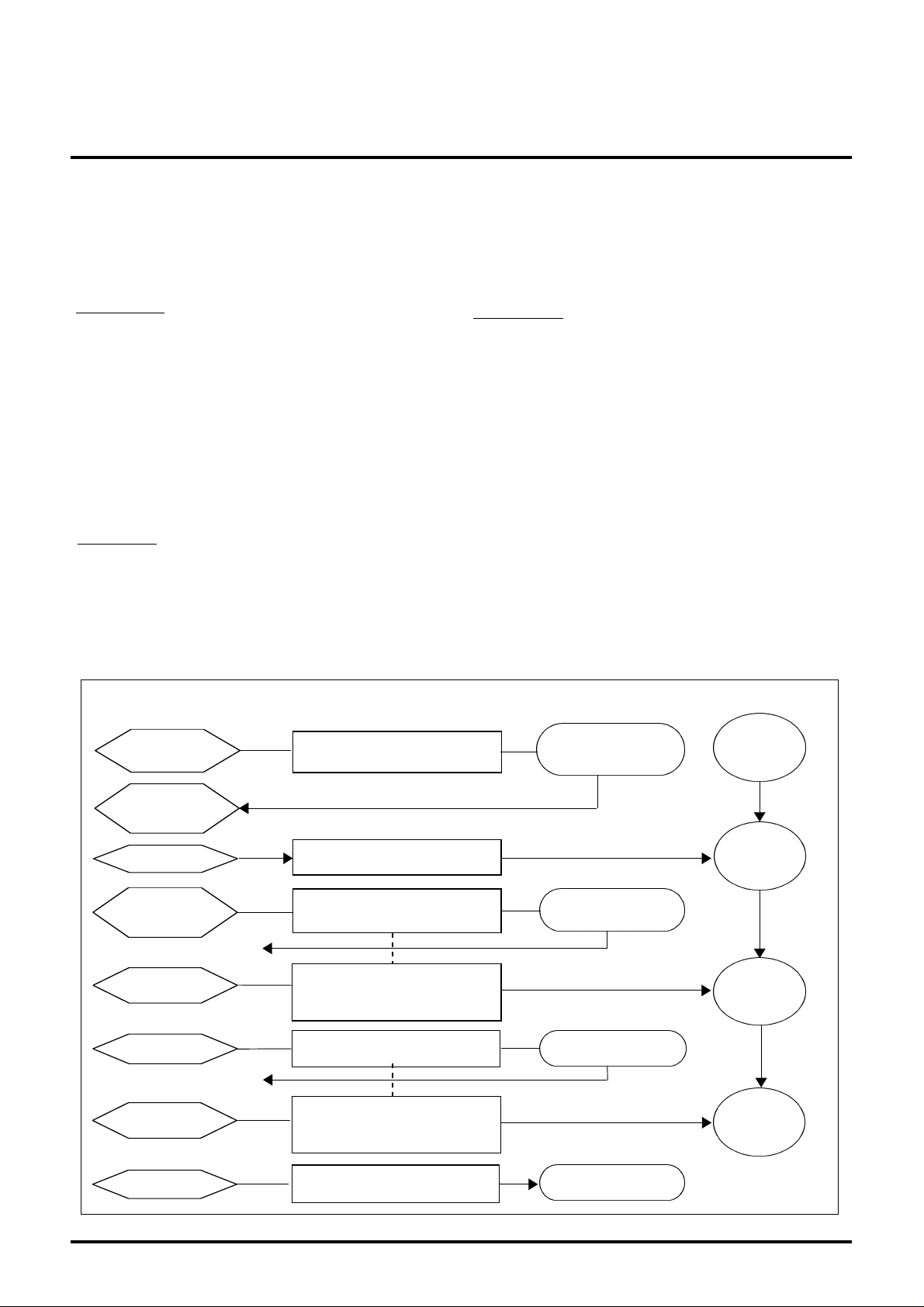
Figure 3. Abstract of enumeration operations
To both control read and control write, buffer size of
M66290AGP/FP
(3) Control transfer / Enumeration
In control transfer, there are setup stage, data stage,
and status stage.
M66290A manages stage and inform CPU the stage
shift by interrupt. CPU do stage transact of control
transfer according to the interrupt factor.
Setup stage
In setup stage, 8Bytes request (setup data) of setup
transaction data packet which transferred from host
is stored into four registers automatically (Request,
Value, Index, and Length register).
Except for device state shift request (Set Address and
Set Configuration) which can cope with by the automatic
response control function, analysis (decode) and
execution of contents of request must be done by CPU.
By executing the request, it proceeds to data stage or
to status stage.
Data stage
Data stage executes IN transaction or OUT transaction
according to the contents of request. If it is control
write transfer, data stage is OUT transaction and CPU
prepares for data receive at the timing of interrupt in
If it is control read transfer, data stage is IN transaction
and CPU prepares for data transmit (write into endpoint
FIFO) at the timing of interrupt in setup stage.
M66290A is equipped with control transfer continuous
transmit and receive function. After ended data stage,
it proceeds to status stage.
Status stage
Status stage executes receive/transmit of Null data
(data length 0), in both control write and control read
transfer. Receive/transmit of Null data is possible to
set control transfer complete enable bit (CCPL) after
ended setup stage.
Control transfer complete enable bit is reset when
received setup packet.
Control transfer executes data transfer using EP0.
EP0 can be set by a unit of 64Bytes by "Control
Transfer Control Register".
Access to EP0_FIFO data register must be done by
CPU access. DMA transfer can not be set.
Figure 3. shows the abstract of enumeration
operations.
FIFO when data receive ended.
USB bus connect
Full speed
device recognition
USB reset
USB request
(Control transfer)
USB request
USB request
USB request
M66290A Device firmware
Vbus interrupt
DVST interrupt
Get xx command
CTRT interrupt
Set Address
CTRT/DVST interrupt
(Automatic response available)
Get xx command
CTRT interrupt
Set Configuration
CTRT/DVST interrupt
(Automatic response available)
Clock ON
Initializing
Tr ON
Set response data
Set response data
Device state
Idle
(Powered)
Default
state
Address
state
Configured
state
USB request
Set xx command
CTRT interrupt
Read received data
20

USB DEVICE CONTROLLER
Auto-response control function
of control transfer operations
MITSUBISHI <DIGITAL ASSP>
M66290AGP/FP
M66290A has auto-response function to device
state transition request (Set Address and Set
Configuration)in control transfer.
By the set of "Auto-response Control Register",
auto-response mode to Set Address and to
Set Configuration can be set individually.
If the auto-response mode is set, device state
transition request can be ended without occurring
interrupt.
Continuous transfer function
M66290A has continuous transfer function to
transmit/receive continuously of requested data
Transfer direction of packet :
(1) Continuous receive mode (control write transfer)
Setup
stage
Data
stage
Setup token
OUT token
OUT token
OUT token
OUT token
Data packet
Data packet
Data packet
Data packet
Data packet
ACK
NAK
NAK
ACK
ACK
which extend plural of transaction.
If continuous transfer mode is set, it can transfer the
transmit which data length is set to "EP0 Continuous
Transmit Data Length Register", without
occurring interrupt.
Control read buffer can be set up to 256Bytes at a unit
of 64Bytes. Control write buffer can receive continuously
up to 255Bytes, so secure the area of 256Bytes.
Abstract
Figure 4. shows examples of abstraction of control
transfer operations.
Host to M66290A
INT1:
INT1
CTRT interrupt (setup stage completion)
Read EP0 request and confirm the contents of request.
By receiving SETUP token packet, response PID of
EP0 is set to NAK automatically.
By the set of response PID to BUF (buffer control),
data receive starts.
M66290A to Host
Status
stage
OUT token
IN token
IN token
IN token
INT2
Data packet
NAK
NAK
Null data packet
ACK
ACK
(2) Continuous transmit mode (control read transfer)
Setup
stage
Data
stage
Status
stage
Setup token
IN token
IN token
IN token
IN token
IN token
OUT token
Data packet
NAK
NAK
NAK
Data packet
Data packet
Data packet IN token
Null data packet
ACK
ACK
ACK
ACK
ACK
INT2:
CTRT interrupt (control write transfer status stage shift)
Confirm the number of byte of received data and read
the received data.
By the set of CCPL, transmit the Null data.
Interrupt, which is occurred by control write transfer
status stage shift and by control transfer completion is
different by interrupt enable setting.
INT1:
INT1
CTRT interrupt (setup stage completion)
Read EP0 request and confirm the contents of request.
By receiving SETUP token packet, response PID of
EP0 is set to NAK automatically.
Executes transmit data write which is requested,
set transmit data length, set response PID to BUF
(buffer control), and data transmit is started.
By the set of CCPL, ACK handshake is executed
when received Null data.
Interrupt which is occurred by control read transfer
status stage shift and by control transfer completion is
different by interrupt enable setting.
Figure 4. Examples of abstract of control transfer operations
21

USB DEVICE CONTROLLER
MITSUBISHI <DIGITAL ASSP>
M66290AGP/FP
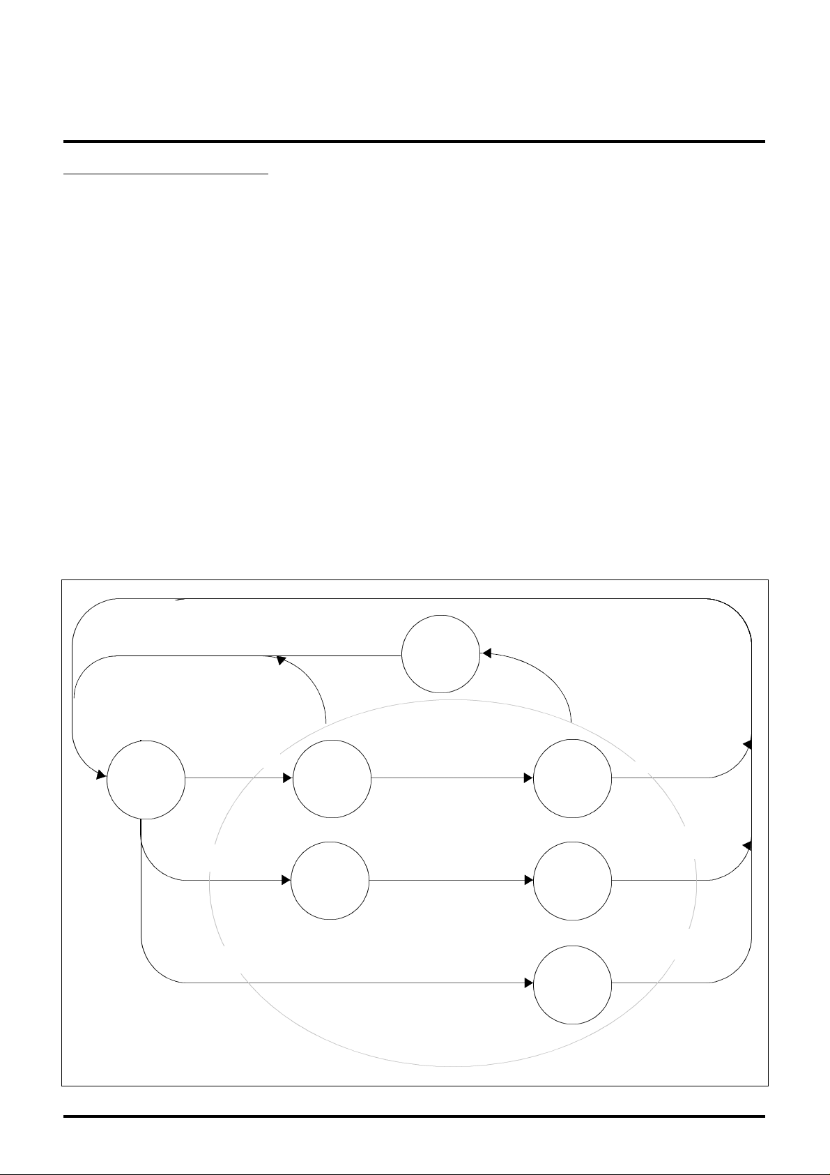
Device state transition
M66290A manages device state by H/W.
It manages Powered, Default, Address, Configured,
and Suspended state of USB device state.
To Set_Address and Set_Configuration request in
auto-response mode, transfer can be completed
without occurring interrupt to CPU.
To Set_Address request, auto-response is executed to
Set_Address request (DeviceAddess=01h
to 7Fh) which device state is in Default state, and to
Powered
state
(DVSQ="000")
USB reset detection (DVST)
USB reset detection (DVST)
other state and to Set_Address request which DeviceAddess
is not equal to 01h to 7Fh, auto-response is not executed.
To Set_Configuration request, auto-response is executed
to Set_Configuration request (ConfigurationValue is not equal
to 0) which device state is in Address state and to
Set_Configuration request (ConfigurationValue=0) which device
state is in Configured state.
To other state and to Set_Configuration request which is
different of its ConfigurationValue from the value above,
auto-response is not executed.
Suspend detection (DVST)
Suspended
state
(DVSQ="100")
Resume detection (RESM)
Suspend detection (DVST)
Default
(DVSQ="001")
Set Address execution (DVST)
(DeviceAddress=01h to 7Fh)
*Can be set to auto-response
Default
(DVSQ="010")
Set Configuration execution (DVST)
(Configuration Value is not equal to 0)
*Can be set to auto-response
Default
(DVSQ="011")
state
Resume detection (RESM)
Suspend detection (DVST)
state
Resume detection (RESM)
Set Configuration execution (DVST)
(Configuration Value is not equal to 0)
*Can be set to auto-response
Suspend detection (DVST)
state
Suspended
state
(DVSQ="101")
Suspended
state
(DVSQ="110")
Suspended
state
(DVSQ="111")
Figure 5. Device state shift
Resume detection (RESM)
22
USB DEVICE CONTROLLER
(Control write transfer
status stage transition)
(Control read transfer
status stage transition)
(Setup stage complete)
(Setup stage complete)
ACK receive
(Control transfer
complete
)
ACK receive
(Control transfer
complete
)
ACK receive
(Control transfer
complete
)
Control transfer stage transition
(Setup stage complete)
M66290A manages control transfer sequence by H/W.
There are setup stage, data stage, and status stage in
control transfer stage, as shown in figure 6. And when
stage shifts, CTRT interrupt occurs.
There are five factors in CTRT interrupt, that is, setup
stage end, control write transfer status stage shift,
control read transfer status stage shift, control transfer
end, and control transfer sequence error. And there are
seven errors as follows in control transfer sequence
error which can be detected by H/W.
If H/W detected control transfer sequence error,
response PID is set to STALL("1x") automatically.
1. IN token packet receive in control write data stage
(In token packet receive which did not do ACK
handshake once to OUT token packet in data stage)
MITSUBISHI <DIGITAL ASSP>
M66290AGP/FP
3. OUT token packet receive in control read data stage.
(OUT token packet receive which did not do data transfer
once to IN token packet in data stage).
4. IN token packet receive in control read status stage.
5. Data packet receive except for Null data in control
read status stage.
6. OUT token packet receive in control write no data
status stage.
7. Data receive which exceeds maximum packet size.
In control write data stage, it can not be recognized as
sequence error when received data packet which exceeds
request wLength value.
2. OUT token packet receive in control write status stage
Receive
setup packet
ACK transmit
Control
Setup
stage
write
data
stage
ACK transmit
Control
read
data
stage
Control
transfer
sequence
error
Receive short packet
or Receive IN token
Transmit short packet
or Receive OUT token
Error detected
Control
write
status
stage
Control
read
status
stage
Figure 6. Stage shift of control transfer
ACK transmit
Control
write
no data
status
stage
23

USB DEVICE CONTROLLER
MITSUBISHI <DIGITAL ASSP>
0000h
15 to 0
0000h
(3-1) Request Register
(
Address : 20h
)
(3-2) Value Register
(
Address
:
22h
)
(3-3) Index Register
(
Address
:
24h
)
(3-4) Length Register
(
Address
:
26h)USB DEVICE CONTROLLER
M66290AGP/FP
bRequest[7:0] bmRequestType[7:0]
D0D1D2D3D4D5D6D7D8D9D10D11D12D15 D13D14
Bit
15 to 8
7 to 0 RequestType
Bit
15 to 0
Bit
Name
bRequest
[7:0]
bmRequest
Type
[7:0]
Bit
Name
wValue
[15:0]
Name Function W/R
register
Name Function W/R
This fields provides bRequest of the last setup packet received.Request register
This fields provides bmRequest of the last setup packet received.
wValue[15:0]
Reset
USBS/WH/W
-00h00hR
-00h00hR
D0D1D2D3D4D5D6D7D8D9D10D11D12D15 D13D14
Reset
USBS/WH/W
R This fields provides wValue of the last setup packet received.Value register
--
wIndex[15:0]
Bit
Bit W/R
15 to 0
Bit
Name
wIndex
[15:0]
Bit
Name
wLength
[15:0]
Name Function W/R
wLength
FunctionName
D0D1D2D3D4D5D6D7D8D9D10D11D12D15 D13D14
Reset
USBS/WH/W
--0000hR This fields provides wIndex of the last setup packet received.Index register
D0D1D2D3D4D5D6D7D8D9D10D11D12D15 D13D14
Reset
USBS/WH/W
R This fields provides wLength of the last setup packet received.Length register
--
24

MITSUBISHI <DIGITAL ASSP>
[6:0]
Reset
(3-5) Control Transfer Control Register
(
Address
:
28h
)
(3-6) EP0 Packet Size Register
(
Address
:
2Ah)USB DEVICE CONTROLLER
M66290AGP/FP
CTRR CTRWCtr_Rd_Buf_Nmb[5:0] Ctr_Wr_Buf_Nmb[5:0]
D0D1D2D3D4D5D6D7D8D9D10D11D12D15 D13D14
Bit Name
14
13 to 8
7
6
5 to 0
Bit
Name
Reserved
Ctr_Rd_
Buf_Nmb
[5:0]
CTRW
Reserved
Ctr_Wr_
Buf_Nmb
[5:0]
Control read
transfer continuous
transmit mode
Control read buffer
start number
Control write
transfer continuous
receive mode
Control write buffer
start number
Function W/R
Control read transfer continuous transmit mode is set
when "1" is written in this bit.
Write/Read "0"
Appoint the start number of the buffer which is used in control read
transfer by a unit of 64bytes.
The buffer is available from #00h to #2Fh.
When control read continuous transmit mode is set, it can
transmit continuously up to 255Bytes, so keep the area of the
buffer of 256Bytes (4 blocks).
When "1" is written, control write transfer continuous receive mode
is set.
Write/Read "0"
Appoint the start number of the buffer which is used in control write
transfer by a unit of 64bytes.
The buffer is available from #00h to #2Fh.
When control write continuous receive mode is set, it can receive
continuously up to 255bytes, so keep the area of buffer of 256bytes
(4 blocks).
Reset
USBS/WH/W
--0W/RCTRR15
--00hW/R
--0W/R
--00hW/R
Bit Name Function W/R
15 to 7 Reserved
6 to 0
Bit
Name
EP0_MXPS
Max Packet size
EP0_MXPS[6:0]
Write/Read "0"
Set the maximum value of data (byte) which transmit or receive in a
packet transfer.
Set the value of wMaxPacketSize in request.
This bit must be set after set the response PID to NAK("00").
25
D0D1D2D3D4D5D6D7D8D9D10D11D12D15 D13D14
USBS/WH/W
--08hW/R

MITSUBISHI <DIGITAL ASSP>
(3-7) Auto-response Control Register (Address : 2Ch)
(3-8) EP0_FIFO Selection Register (Address : 30h)
M66290AGP/FP
D0D1D2D3D4D5D6D7D8D9D10D11D12D15 D13D14
ATADASCN
Bit
Name
15 to 2 Reserved
ASCN
1
ASTD
0
NameBit
Set_Configuration
Auto-response
mode
Set_Address
Auto-response
mode
Function W/R
Write/Read "0"
When "1" is written into this bit, auto-response mode of
Set_Configuration request is set.
To the Set_Configuration request in auto-response mode,
transfer can be completed without occurring interrupt to CPU.
(Set of CCPL is not needed)
Auto-response is done to the Set_Configuration request
(ConfigurationValue is not equal to 0) in Address device state
and to the Set_Configuration request (ConfigurationValue is equal to 0)
in Configured state.
To the other state and to the Set_Configuration request which
ConfigurationVale is different from the value above, auto-response
is not done.
When "1" is written into this bit, automatic response mode of
Set_Address request is set.
To the Set_Address request in automatic response mode,
transfer can be completed without occurring the interrupt to
CPU. (Set of CCPL is not needed)
Automatic response is done to the Set_Address request (DeviceAddress
is equal to 01h to 7Fh) which device state is Default state.
To the other state and to the Set_Address request which DeviceAddress
is not equal to 01h to 7Fh, automatic response is not done.
Reset
USBS/WH/W
--0W/R
--0W/R
OctlRCNT ISEL
Bit Name W/R
15
14 to 11
0
Bit
Name
RCNT
Reserved
Octl10
Reserved9-1
ISEL
Read count mode
FIFO access
8 bit mode
Buffer select
If this bit is "1", every time when read EP0_FIFO register,the value of
ODLN register is counted down.
Write/Read "0"
If this bit is set to "1", data register of FIFO turns to 8-bit mode and
lower 8 bit[7:0] becomes enable when access the "FIFO Data Register"
of endpoint.
When transmit data of odd number byte, data must be written in 8-bit
mode.
When read in 8-bit mode, set to 8-bit mode before data receive.
Write/Read "0"
0 : Control write (OUT) buffer select
1 : Control read (IN) buffer select
Function
D0D1D2D3D4D5D6D7D8D9D10D11D12D15 D13D14
Reset
USBS/WH/W
--0W/R
--0W/R
--0W/R
26

USB DEVICE CONTROLLER
MITSUBISHI <DIGITAL ASSP>
(3-9) EP0_FIFO Control Register
(
Address
:
32h)USB DEVICE CONTROLLER
M66290AGP/FP
CCPLEP0_PID[1:0] E0reqBCLRIVAL ODLN[7:0]
D0D1D2D3D4D5D6D7D8D9D10D11D12D15 D13D14
Bit
15 to 14
13
Bit
Name
EP0_PID
[1:0]
IVAL
Response PID
In buffer status
FunctionName
Setting the response PID.
00 : NAK Whatever the buffer state is,do NAK handshake.
01 : BUF Response PID is selected by the state of buffer
and sequence toggle bit status.
(One of ACK, NAK, and DATA0/DATA1)
1x : STALL Do STALL handshake
1. When received Setup packet, turns to "00"(=NAK) automatically.
2. When received request (Set_Address, etc.) which is set to
automatic response, turns to "01"(=ACK) automatically after
completed the Setup transaction.
3. If sequence error occurred in control transfer,or received data
in control write transfer which exceed maximum packet size,
this turns to "1x"(=STALL) automatically.
If the control read buffer is selected, this becomes IN buffer
effective state flag.
When set to "1", it becomes to transmit data set state (SIE read enabled).
If data is written which exceeds to the maximum byte of maximum
packet size (MXPS), this bit is set to "1".
When short packet transmit, set this bit to "1" after wrote transmit data.
If the IVAL="1" and BCLR="1" is written at the same time,
IN buffer effective state flag is set.
(This is effective to transmit 0 length data)
If the control readout) buffer is selected, it becomes OUT buffer
effective state status.
Status "1" shows that there is data which can be read.
This bit shows the effective value when E0req bit is "0".
If "1" is written, it is not changed.
If "0" is written, flag is not changed.
W/R
Reset
USBS/WH/W
--00W/R
--0W/R
BCLR
12
11
EP0_FIFO readyE0req
Buffer clear
If "1" is written into this bit When the selected endpoint is set to IN, IN
buffer effective state flag and the data (byte) which is written are cleared.
If IVAL="1" and BCLR="1" is written at the same time, data is cleared
but IN buffer effective state flag is set.(This is effective to transmit 0
length data)
When "1" is written into this bit, if the selected endpoint is set to OUT,
OUT buffer effective state flag is cleared and read data is also cleared.
When "0" is written, this bit is not changed.
If this bit is "0", access to EP0_FIFO data register is enabled.
And when this bit is "0", IVAL and ODLN bit shows the effective value.
EP0_FIFO data register, when read or write, needs cycle time of
200ns (min).
(Continuous access at 5MHz is available)
27
--0W/R
--1R

MITSUBISHI <DIGITAL ASSP>
(3-10) EP0_FIFO Data Register
(
Address
:
34h
)
(3-11) EP0 Continuous transmit Data Length (Address : 36h)
M66290AGP/FP
Bit
9 to 8
7 to 0
Bit
Name
CCPL10
Reserved
ODLN
[7:0]
Name Function
To write "1" into this register, status stage of control transfer can be
completed.
Control transfer
complete enable
Control write
receive
data length
If this bit is "1" and response PID is BUF("01"), Null data is transmitted
in control write transfer, and do response ACK in control read transfer
when received NULL data.
If this bit is "0", do response NAK in status stage.
This flag is reset to "0" when received setup packet.
Write/Read "0"
Received data length(byte) can be read from this register.
If RCNT mode is set, every time when read EP0_FIFO data register,
it is counted down by -1(8-bit mode) or by -2(16-bit mode).
This bit shows effective value when E0req bit is "0".
EP0_FIFO[15:0]
W/R
Reset
USBS/WH/W
--0W/R
--00hR
D0D1D2D3D4D5D6D7D8D9D10D11D12D15 D13D14
Bit
15 to 0
Bit
7 to 0
Bit
Name
EP0_FIFO
[15:0]
Bit
Name
Reserved14-8
SDLN
[7:0]
Name Function W/R
When read, this becomes to receive data FIFO register.
If it is set to 8-bit mode, lower 8 bit[7:0] is valid.
When write, this becomes to transmit data FIFO register.
EP0_FIFO data
Name
Control read
continuous transmit
data length
If it is set to 8-bit mode, lower 8 bit[7:0] is valid.
Both for read and write, cycle time of 200ns (min) is needed.
(Continuous access at 5MHz is available)
Read when IN buffer is selected or write when OUT buffer is
selected is inhibited.
SDLN[7:0]
Function W/R
Write/Read "0"
Set the control read continuous transmit data length (byte).
It can be set up to FFh (255bytes).
In control read continuous transmit mode, write FIFO data (transmit data)
after set this register.
This is available in control read continuous transmit mode.
Reset
USBS/WH/W
--xxxxW/R
D0D1D2D3D4D5D6D7D8D9D10D11D12D15 D13D14
Reset
USBS/WH/W
--00hW/R
28

USB DEVICE CONTROLLER
(Toggle buffer)
FIFO area:256Bytes(4 blocks)
FIFO area:256Bytes(4 blocks)
FIFO area:64Bytes(1 block)
FIFO area:64Bytes(1 block)
FIFO area:128Bytes(2 blocks)
FIFO area:2kBytes(32 blocks)
(4) Endpoint and FIFO control
hese five endpoints (EP1 to EP5) can be set to
Built-in FIFO for endpoint buffer is 3kBytes totally of its
receives short packet. If the data to be received is data
and if the data is data packet (max packet size) which is
to set IVAL flag to transmit a multiple data of maximum
Except for EP0 for control transfer, M66290A can set
five endpoints as EP1 to EP5.
Each of t
bulk, interrupt, and isochronous transfer. And yet,
another constitution can configurated independently.
Below are the constitutions to be realized.
memory capacity. This FIFO of 3kBytes can divided
into each endpoint of EP0 to EP5 and to each endpoint,
can assign up to 1024Bytes (max) by a unit of 64Bytes.
Buffer size of each endpoint must be set to over the
capacity which is set in maximum buffer size.
In the buffer size, which is set, bytes of maximum
packet size is used for valid. (If set the buffer size to
128Bytes to the endpoint which maximum packet size
is set to 64Bytes, 64Bytes are valid)
We show setting examples to each of these buffer of
EP0 to EP5 below, and next explain about continuous
transmit and receive function, FIFO control, DMA
transfer, and double buffer.
Continuous transfer function
Continuous transfer function is to transmit/receive data
which extend plural transaction without occurring interrupt
to CPU.
For EP1 to EP5, this function is effective when transfer
type is bulk transfer.
In each endpoint, when continuous transfer mode is set,
it can transfer data up to the buffer size which is set to
the endpoint without occurring interrupt to CPU.
Construction of endpoint (EP1 to EP5) FIFO
Register
Transfer type EPi_TYP[1:0]
Transfer direction
Double buffer
Continuous
transmit/receive
Buffer size
Response PID EPi_PID[1:0]
DMA transfer EPi_DMAE
Receive data
read and abandon
mode
Max packet size EPi_MXPS[9:0]
EPi_DIR Can be set to IN/OUT
EPi_DBLB
EPi_RWMD
EPi_Buf_siz[3:0]
EPi_ACLR
EP1 to EP5
Can be set to Bulk,
Interrupt, isochronous
transfer.
Can be set
Can be set
(Effective in bulk transfer)
Can be set
(Up to 1024bytes by
a unit of 64bytes)
Can be set to
NAK, STALL, and
BUF(buffer control).
Can be set
Can be set
Can be set
( 0 to 1023bytes)
MITSUBISHI <DIGITAL ASSP>
M66290AGP/FP
To use with double buffer constitution, 1kBytes x2
maximum of buffering is realized.
Continuous receive mode can receive data packet
continuously up to the buffer size which is set, or until
packet of max packet size, it can receive continuously
up to the buffer size without occurring interrupt to CPU,
less than buffer size, interrupt to CPU is not occurred.
In bulk transfer, when set max packet size as 64Bytes,
buffer size as 1024Bytes, and FIFO constitution as
double buffer, when received data of max packet size
as 16 times (1024Bytes), it became buffer redried
enable) and urge to CPU by interrupt to read received
data. When received short packet, ends the continuous
receive and buffer became redried enable).
Continuous transmit mode can transmit data packet
continuously up to buffer size which is set. Short packet
transmit can be done to set IVAL flag. And it is needed
packet size which is less than buffer size.
By set Null data transmit addition mode, when write a
multiple data of max packet size into buffer and
transmit, Null data can be transmitted automatically
after the last packet is transmitted .
Examples of endpoint FIFO setting
FIFO
number
00h to
03h
04h to
07h
08h
09h
0Ah to
0Bh
0Ch to
0Fh
10h to
2Fh
Memory
address
000h to
0FFh
100h to
1FFh
200h to
23Fh
240h to
27Fh
280h to
2FFh
300h to
3FFh
400h to
BFFh
Endpoint setting
EP0:Control write transfer
Buffer size:256Bytes
Control write continuous receive
mode(CTRW)
EP0:Control read transfer
Buffer size:256Bytes
Control read continuous transmit
mode(CTRR)
EP2:Interrupt transfer(IN)
Buffer size:64Bytes
EP4:Interrupt transfer(OUT)
Buffer size:64Bytes
EP3:Bulk transfer(IN)
Buffer size:64Bytes
Double buffer constitution(DBLB)
Not used:256Bytes(4 blocks)
EP1:Bulk transfer(OUT)
Buffer size:1024Bytes
Double buffer constitution(DBLB)
Continuous receive mode(RWMD)
29

USB DEVICE CONTROLLER
MITSUBISHI <DIGITAL ASSP>
D0D1D2D3D4D5D6D7D8
D9
D10
D11
D12
D13
D14
D15
M66290AGP/FP
FIFO control
Access to endpoint buffer of EP0 to EP5 is done by
three FIFO data registers. One is only for EP0 and
Others are common to EP1 to EP5. Common data
registers are divided into two, because accessing
is different, that is for CPU access and for DMA
transfer. Which endpoint of EP1 to EP5 to be
accessed can be selected to set each FIFO
selection register.
Endpoint
EP0
EP1 to EP5
Accessing
CPU access
CPU access
DMA transfer
Register name
EP0_FIFO
data register
CPU_FIFO
data register
DMA_FIFO
data register
Each of three FIFO registers has functions as
follows. And these functions can be used to set
"Each FIFO Selection/Control Register".
Short packet transmission function
(IVAL : IN buffer status bit)
Transmit/receive buffer clear function
(BCLR : Buffer clear bit)
Null data (data length 0) transmit function
(IVAL & BCLR)
Data length (8/16 bit) set function
(Octl : Register 8bit mode bit)
Received data length count down function
(RCNT : Read count mode bit)
*: There is none for DMA transfer
Access to CPU_FIFO data register when interrupt
occurred, to know the endpoint which requested
access, access the "Interrupt Status Register 0/1"
and by checking the interrupt status flag and know
the endpoint which requested access, and then set
endpoint to be accessed by "CPU_FIFO Selection
Register".
If there is no change of endpoint setting, it is not
needed to set again the CPU access endpoint
appointment bit.
Data transfer procedure
Data which is set to endpoint FIFO, is sent to USB
bus by LSB first. When store the received data
from USB bus to endpoint FIFO, it is as the same
as above.
1
Time scale
DMA transfer
To endpoint of EP1 to EP5, 16bits width or 8bit width of
DMA
transfer is available.
Each endpoint of EP1 to EP5 can be set to CPU access
mode or DMA access mode by set of "EPx Configuration
Register 1" mentioned later.
DMA transfer is realized to hand shake with external DMAC
and Dreq, Dack signal. Dreq is asserted when endpoint
buffer, which is set to DMA transfer mode, became ready.
The means of Buffer ready state is, if the endpoint
transfer
direction is set to Out (recive data from host) buffer ready
means that in read enable state, if the endpoint transfer
direction is set to IN(transmit data to host) buffer ready
means that in write enable state. Setting the transfer
direction can be done by "EPi Configuration Register 0" to
each endpoint.
When Dack comes from external DMAC after asserted
Dreq, Dreq is negated.
In DMA transfer, Dack is dealt equivalently with CS signal
and DMA_FIFO address appointment.
Appoint read or write operation by RD or WR signal.
This DMA transfer can be used only for single transfer,
which
transfers one word (16bit or 8bit) by one time Dreq start.
In DMA transfer, as same as the CPU access, occurs
endpoint buffer not ready interrupt and endpoint buffer
empty interrupt according to endpoint buffer state. But as
to endpoint buffer ready interrupt, it is not same as the
CPU access as follows.
In DMA transfer, endpoint buffer ready interrupt is not
occurred if the transfer direction is IN.
If the transfer direction is OUT, interrupt is occurred when
received short data packet and ended data transfer of all
data which received in DMA transfer.
Occurring of endpoint buffer ready interrupt and to refer
DMA_DTLN, it can be known that short data packet was
received.
DMA_DTLN shows the number of byte of short data
packet,
or in the continuous receive mode it shows the number of
byte
of received data before short data packet receive.
16
(Data send procedure to USB bus)
30

USB DEVICE CONTROLLER
Endpoint buffer status
Double buffer operations
The endpoint FIFO of EP1 to EP5 can be
So a double of transfer data of its buffer size, which
set to double buffer constitution.
is set, can be stored.
(1) Receiving
Below are the receive status examples
of the endpoint which is set to double buffer.
MITSUBISHI <DIGITAL ASSP>
M66290AGP/FP
"Data1" receive start
"Data1" receive end
"Data2" receive start
"Data1" read start
Before "Data1" read end
"Data2" receive end
"Data1" read end
When data receive ended, the buffer
is set to Ready state (read enable)
and occurs INTR interrupt
Continuous receiving is available
before data read.
In OUT token receive to this
endpoint, M66290A occurs
INTN interrupt and do NAK
handshake.
It becomes receive enable
after read of data1 ended.
And occurs INTR interrupt
because the buffer is ready.
USB side
IN
receiving data
IN
data2
IN
data2
data receive completed
data receive impossible
data receive enable data read available
Buffer1 Buffer2
data1
Buffer2 Buffer1
data1
data receive
available
Buffer2 Buffer1
receiving data
Buffer2 Buffer1
data2
receiving data
Buffer2 Buffer1
Buffer1 Buffer2
data receive completed
data read available
data1
data read available
reading data
reading data
data2
CPU bus side
data1
data1
OUT
OUT
After "Data1" read end
"Data2" receive end
"Data3" receive start
Figure 7. Double buffer activities-1
M66290A Occurs INTR interrupt
because the buffer is ready.
31
Buffer1 Buffer2
data2
data receive available data read available
IN
Buffer1 Buffer2
data3
receiving data
data
data read available
: Data exists in buffer
data2

USB DEVICE CONTROLLER
In token receive
(2) Transmitting
Endpoint buffer status
Below are the transmit status examples
of the endpoint which is set to double buffer.
MITSUBISHI <DIGITAL ASSP>
M66290AGP/FP
"Data1" write start
"Data1" write end
"Data1" transmit start
"Data2" write start
Before "Data1" transmit end
"Data2" write end
"Data1" transmit end
Can not transmit because the
transmit buffer is in NotReady.
Request CPU to prepare transmit
data by INTN interrupt
End of data write of maximum packet
size or to set(short packet transmit)
IVAL flag, it becomes transmit data
set status, and transmit becomes enable.
And occurs INTR interrupt because
the buffer is in Ready (write enable).
Data write is available during
data transmitting.
End of data write of maximum packet
size or to set (short packet transmit)
IVAL flag, it becomes transmit data
set status, and transmit becomes enable.
When data transmit ended,
it occurs INTR interrupt
because the buffer is in
Ready.
USB side
data transmit impossible
data transmit impossible
data transmit available
OUT
transmitting data
OUT
data1
transmitting data
data transmit avalable data write avalable
Buffer1 Buffer2
data write available
Buffer1 Buffer2
writing data
Buffer2 Buffer1
data1
data write available
Buffer2 Buffer1
data1
writing data
Buffer2 Buffer1
data write completed
data writeimpossible
Buffer1 Buffer2
data2
CPU bus side
data1
data2
data2
IN
IN
IN
After "Data1" transmit end
"Data2" write end
When data transmit ended, it occurs
INTR interrupt because the buffer
is in Ready.
"Data3" write start
Figure 8. Double buffer activities-2
Buffer1 Buffer2
data2
data transmit avalable
Buffer1 Buffer2
data2
data transmit avalable
data
: Data exists in buffer
data write avalable
data3
writing data
IN
32

USB DEVICE CONTROLLER
MITSUBISHI <DIGITAL ASSP>
(4-1) CPU_FIFO Selection Register (Address : 40h)
(4-2) CPU_FIFO Control Register (Address : 42h)
M66290AGP/FP
D0D1D2D3D4D5D6D7D8D9D10D11D12D15 D13D14
CPU_EP[3:0]RCNT
Name
15 RCNT
Reserved14 to 4
CPU_EP
3 to 0
[3:0]
Bit
NameBit
Read count mode
CPU access
endpoint
Function W/R
If this bit is "1", every time when read CPU_FIFO register,
CPU_DTLN register value is counted down.
Write/Read "0"
Appoint the CPU access endpoint.
"0001"=EP1,"0010"=EP2,"0011"=EP3,
"0100"=EP4,"0101"=EP5
EP0 can not be appointed.
Don't change the setting in writing (IN) or in reading (OUT).
Change of the setting of the endpoint of direction IN must be
done after confirmed that IVAL="0" and Creq="0", or IVAL="1"
and Creq="1".
Change of the setting of the endpoint of direction OUT must
be done after confirmed that IVAL="1" and Creq="0", or
IVAL="0" and Creq="1".
CPU_DTLN[10:0]CreqBCLRIVAL
Reset
USBS/WH/W
--0W/R
--0000W/R
D0D1D2D3D4D5D6D7D8D9D10D11D12D15 D13D14
Reserved15, 14
Bit
Name
Write/Read "0"
If the selected endpoint is set to IN, this becomes IN buffer
effective state flag.
When set to "1", it becomes transmit data set state.
(SIE is available to read)
When the data (byte) which exceeds to the maximum packet size
(MXPS) is written, this bit is set to "1".
In short packet transmit, set this bit to "1" after wrote the transmit data.
If IVAL="1" and BCLR="1" is written at the same time, the
IN buffer statusIVAL13
effective state flag is set.
(This is effective to transmit 0 length data)
If the selected endpoint is set to OUT, it becomes to
OUT buffer effective state status.
Status "1" shows that there is data which is available to read.
When Creq bit is "0", this bit shows effective value.
This bit is not changed when "1" is written.
Flag is not changed when "0" is written.
Bit Name W/R
Function
Reset
USBS/WH/W
--0W/R
33

USB DEVICE CONTROLLER
MITSUBISHI <DIGITAL ASSP>
M66290AGP/FP
Bit
12
11
Bit
Name
BCLR
Creq
Name Function
If the selected endpoint is set to IN, when "1" is written into
this bit, the IN buffer effective state flag and the data (byte)
which is written are cleared.
If IVAL="1" and BCLR="1" is written at the same time, data
is cleared but the IN buffer effective state flag is set.
(This is effective to transmit 0 length data)
Buffer clear
CPU_FIFO ready
If the selected endpoint is set to OUT, when "1" is written into
this bit, the OUT buffer effective state flag and the read data (byte)
are cleared.
If it is set to double buffer, the state of write/read enable buffer
for CPU is cleared.
To set the EPi_ACLR, USB bus buffer is cleared.
This bit is not changed when "0" is written.
If this bit is "0", access to CPU_FIFO data register is available.
And if this bit is "0", the bit of IVAL and CPU_DTLN bit shows the
effective value.
When read or write to CPU_FIFO register, 200ns (min) of cycle
time is needed. (Continuous access at 5MHz is available)
If the access end point is changed, 200ns (min) of recovery
time is needed.
W/R
Reset
USBS/WH/W
--0W/R
--1R
CPU_FIFO
receive data
length
10 to 0
CPU_DTL
N[10:0]
When read this register, receive data length (byte) appears.
When RCNT mode is set, every time when read CPU_FIFO
register, it is counted down by -1 (8-bit mode) or by -2 (16-bit mode).
If RCNT mode is not set, this register turns to 000h after all of
received data is read.
This bit shows effective value when Creq bit is "0".
34
--000hR

USB DEVICE CONTROLLER
CPU_FIFO
DMAEN
(4-3) CPU_FIFO Data Register (Address : 44h)
(4-4) DMA_FIFO Selection Register (Address : 48h
)
CPU_FIFO[15:0]
MITSUBISHI <DIGITAL ASSP>
M66290AGP/FP
D0D1D2D3D4D5D6D7D8D9D10D11D12D15 D13D14
Bit
15 to 0
MODE
Bit
Bit
Name
[15:0]
Bit
Name
MODE15
Name Function W/R
If the selected endpoint is set to OUT, this becomes to
receive data FIFO register.
If the selected endpoint is set to IN, this becomes to
transmit data FIFO register.
CPU_FIFO data
DMA operation
mode
If the selected endpoint is set to 8-bit mode, lower 8 bit [7:0] is valid.
When read or write, 200ns (min) of cycle time is needed.
(Continuous access at 5MHz is available)
Read operation when direction IN is appointed or write operation
when direction OUT is appointed, write operation is inhibited.
FunctionName
Set the operation mode of DMA transfer.
0 : High speed transfer mode
1 : One word transfer mode
In high speed transfer mode, when endpoint buffer is in read/write enable
in the state that DMA transfer enable, Dreq is asserted.
In one word transfer mode, when endpoint buffer is in read/write enable
in the state that DMA transfer enable and Dack="H", Dreq is asserted.
In both mode, Dreq detects Dack="L" and is negated.
DMA_EP[3:0]
W/R
Reset
USBS/WH/W
--xxxxW/R
D0D1D2D3D4D5D6D7D8D9D10D11D12D15 D13D14
Reset
USBS/WH/W
--0W/R
Write/Read "0"Reserved14 to 9
DMAEN8
Reserved
7 to 4
DMA_EP
3 to 0
[3:0]
DMA transfer
enable
DMA transfer
endpoint
If this bit is "1", endpoint buffer which is appointed by DMA_EP[3:0]
is enable to write or when read is enable, Dreq is asserted.
If "0" is written in DMA transferring, DMA transfer is forced to end.
Write/Read "0"
Appoint the endpoint for DMA transfer.
"0001"=EP1,"0010"=EP2,"0011"=EP3,
"0100"=EP4,"0101"=EP5
EP0 can not be appointed.
Don't change the setting during write (IN) or read (OUT).
Change of the setting of the endpoint of direction IN must
be done after confirmed that IVAL="0" and Dreq="0", or
IVAL="1" and Dreq="1".
Change of the setting of the endpoint of direction OUT must
be done after confirmed that IVAL="0" and Dreq="1".
--0W/R
--0000W/R
35

USB DEVICE CONTROLLER
MITSUBISHI <DIGITAL ASSP>
(4-5) DMA_FIFO Control Register (Address : 4Ah)
M66290AGP/FP
D0D1D2D3D4D5D6D7D8D9D10D11D12D15 D13D14
DMA_DTLN[10:0]DreqBCLRIVAL
Bit
Name
Reserved15, 14
Bit
Write/Read "0"
If the selected endpoint is set to IN, this becomes IN buffer
effective state flag.
When set to "1", it becomes transmit data set state.
(SIE is available to read)
When the data (byte) which exceeds to the maximum packet size
(MXPS) is written, this bit is set to "1".
In short packet transmit, set this bit to "1" after wrote
the transmit data.
If IVAL="1" and BCLR="1" is written at the same time, the
IVAL13
IN buffer status
IN buffer effective state flag is set to "1".
(This is effective to transmit 0 length data)
If the selected endpoint is set to OUT, it becomes to
OUT buffer effective state status.
Status "1" shows that there is data which is available to read.
When Creq bit is "0", the value of this bit is effective.
This bit is not changed when "1" is written.
Flag is not changed when "0" is written.
FunctionName
W/R
Reset
USBS/WH/W
--0W/R
12 BCLR
Buffer clear
If "1" is written into this bit when the selected endpoint is
set to IN, IN buffer effective state flag and the data (byte)
which is written are cleared.
If the IVAL="1" and BCLR="1" is written at the same time,
the data is cleared but the IN buffer effective state flag
is set.(This is effective to transmit 0 length data)
If "1" is written into this bit when the selected endpoint is
set to OUT, OUT buffer effective state flag and the read data
(byte) are cleared.
If it is set to double buffer, the state of buffer which can
be read or write for CPU bus is cleared.
To set the EPi_ACLR, USB bus buffer is cleared.
This bit is not changed when "0" is written.
--0W/R
36

USB DEVICE CONTROLLER
MITSUBISHI <DIGITAL ASSP>
(4-6) DMA_FIFO Data Register (Address : 4Ch)
M66290AGP/FP
Bit
11
10 to 0
Bit
Name
Dreq
DMA_DT
LN[10:0]
Name Function W/R
If this bit is "0", then access is available to DMA_FIFO register.
DMA_FIFO
ready
DMA_FIFO
receive data
length
And if this bit is "0", then the bit of IVAL and DMA_DTLN is valid.
This bit is used as DMA request signal (Dreq).
When read this register, receive data length (byte) is appears.
This bit is valid when Dreq bit is "0".
DMA_FIFO[15:0]
Reset
USBS/WH/W
--1R
--000hR
D0D1D2D3D4D5D6D7D8D9D10D11D12D15 D13D14
Bit Function W/R
15 to 0
Bit
Name
DMA_FI
FO[15:0]
Name
DMA_FIFO data
If the selected endpoint is set to OUT, this becomes to receive data
FIFO register.
If the selected endpoint is set to IN, this becomes to transmit data
FIFO register.
If the selected endpoint is set to 8-bit mode, lower 8 bit [7:0] are valid.
Read operation when the endpoint appointed direction IN, or
write operation when the endpoint appointed direction OUT, is inhibited.
Reset
USBS/WH/W
--xxxxW/R
37

USB DEVICE CONTROLLER
EPi_DBLB
EPi_ITMD
(4-7) EPi
Configuration Register 0 ( i=1 to 5)
(Address : EP1=60h, EP2=64h, EP3=68h, EP4=6Ch, EP5=70h)
RWMDDBLBEPi_TYP[1:0] DIR ITMD EPi_Buf_siz[3:0] EPi_Buf_Nmb[5:0]
The EPi configuration register 0 must be set in a state of response PID is NAK("00").
MITSUBISHI <DIGITAL ASSP>
M66290AGP/FP
D0D1D2D3D4D5D6D7D8D9D10D11D12D15 D13D14
Bit
15 to 14
13
12
11 to 8
7
Bit
Name
EPi_TYP
[1:0]
EPi_Buf_
siz[3:0]
Transfer type
Transfer directionEPi_DIR
Interrupt toggle
mode
Buffer size
Double buffer mode
FunctionName
To set the transfer type of endpoint.
00 : not Configured
01 : bulk transfer
10 : interrupt transfer
11 : isochronous transfer
To set the transfer direction of endpoint
0 : OUT (receive data from host)
1 : IN (transmit data to host)
When changed the state of transfer direction, clear (EPi_ACLR)
the endpoint buffer.
To set the sequence toggle bit mode of interrupt transfer.
0 : Alternation data toggle bit mode
(Only toggled when transfer completed with no problem)
1 : Continuous toggle bit mode
(Whatever the hand shake exists or the types are, it toggles
every time when data packet is transmitted )
This is effective when endpoint is set to interrupt(IN) transfer.
Set endpoint buffer size at a unit of 64Bytes.
"0000"=64Bytes, "0001"=128Bytes, ...., "1110"=960Bytes,
"1111"=1024Bytes
Set the constitution of endpoint buffer.
0 : Single buffer mode
1 : Double buffer mode
In double buffer mode, double of the buffer size is taken as the endpoint
buffer.
W/R
Reset
USBS/WH/W
--00W/R
--0W/R
--0W/R
--0000W/R
--0W/R
Continuous
EPi_
6
RWMD
EPi_Buf_
5 to 0
Nmb[5:0]
transfer mode
(only for Bulk
transfer)
Buffer start number
If "1" is written into this bit, continuous transfer mode of endpoint is set.
When the direction of endpoint is set to OUT, then it is set to continuous
receive mode. And when the direction of endpoint is set to IN, then it is
set to continuous transmit mode.
Continuous receive mode can receive data packet up to the buffer size
which is set, or can receive continuously before receives short packet.
Continuous transmit mode can transmit data packet up to the buffer size
which is set, and transmission of short packet can be done by set the
IVAL flag.
In data packet (max packet size) receive which is less than buffer
size, interrupt to CPU does not occur.
Continuous transfer mode is effective only in bulk transfer.
Appoint the first number of the buffer of a unit of 64Bytes.
Buffer exists from #00h to #2Fh.
Buffer size(double of the buffer size in double buffer mode), which is
appointed from the first, is secured for endpoint buffer.
Set that plural of endpoint do not occupy the same buffer area.
38
--0W/R
--00hW/R

USB DEVICE CONTROLLER
NULMD
DMAMD
(4-8) EPi Configuration Register 1 ( i=1 to 5 )
(Address : EP1=62h, EP2=66h, EP3=6Ah, EP4=6Eh, EP5=72h)
The EPi configuration register 1 must be set in a state of response PID is NAK("00").
Bit
15, 14
Bit
Name
EPi_
PID
[1:0]
Name Function
Set response PID.
00 : NAK Whatever the buffer state is, do NAK handshake.
01 : BUF Response PID is selected according to the state of buffer
and sequence toggle bit. (In bulk/interrupt transfer, one of
Response PID
ACK, NAK, DATA0, and DATA1)
1x : STALL Do STALL handshake.
If the transfer direction of selected endpoint is OUT, when received
data which exceeded maximum packet size (MXPS), it becomes
"1x" (=STALL) automatically.
MITSUBISHI <DIGITAL ASSP>
M66290AGP/FP
EPi_MXPS[9:0]OctlACLREPi_PID[1:0]
W/R
D0D1D2D3D4D5D6D7D8D9D10D11D12D15 D13D14
Reset
USBS/WH/W
--00W/R
13
12
11
10
EPi_
DMAMD
EPi_
NULMD
EPi_
ACLR
EPi_Octl
DMA transfer mode
Null data
addition
transmit mode
OUT buffer
automatic
clear mode
FIFO access
8 bit mode
Set the access mode to endpoint buffer.
0 : CPU access mode
1 : DMA transfer mode
To set this bit as "1", Null data addition transmit mode is set .
In the endpoint which is set to continuous transmit mode, when
write a multiple data of maximum packet size into buffer and transmit,
Null data is transmitted automatically after transmitted the last packet.
This setting is effective when continuous transmit mode is set.
When the selected endpoint is set to OUT and if this bit is set to "1",
OUT buffer effective flag and read data (number of byte) is cleared.
In this state(OUT buffer does not become effective state), SIE side
writes data from host into OUT buffer but CPU side does not read.
When set this bit to "1", whatever the transfer direction is, endpoint
buffer (all buffer of single/double buffer) are cleared.
When clear the endpoint buffer, set this bit to "1" and then set again to "0".
When this bit is set to "1", FIFO data register becomes 8-bit mode and
when accessed "FIFO Data Register" of endpoint, lower 8bit[7:0]
becomes effective.
When transmit odd number of byte, it is needed to write in 8-bit mode.
When read in 8-bit mode, set to 8-bit mode before data receive.
--0W/R
--0W/R
--0W/R
--0W/R
EPi_
9 to 0
MXPS
[9:0]
Max Packet size
Set the maximum data size (Byte) to transmit/receive in one packet
transfer.
Set the value of wMaxPacketSize in request.
--040hW/R
39

USB DEVICE CONTROLLER
MITSUBISHI <DIGITAL ASSP>
ABSOLUTE MAXIMUM RATINGS
RECOMMENDED OPERATING CONDITIONS
M66290AGP/FP
Symbol
VCC
VI
VO
IO
Pd
Tstg
Symbol
VCC
GND
VI
Supply voltage
Input voltage
Output voltage
Output current
Power dissipation
Storage temperature
Parameter
Supply voltage
Supply voltage
Input voltage
-0.3 to +4.2
-0.3 to VCC+0.3
-0.3 to VCC+0.3
±20
400
-55 to +150
Limits
0
UnitRatingsParameter
V
V
V
mA
mW
C
Max.Typ.Min.
3.63.33.0
VCC0
Unit
V
V
V
VO
Topr
V5.250Input voltage ( Only for Vbus Input )VI(Vbus)
Output voltage
Operating temperature
Normal input
Input rise, fall timetr, tf
Schmidt trigger input
VCC0
+70+250
500
V
C
ns
5
ms
40

USB DEVICE CONTROLLER
MITSUBISHI <DIGITAL ASSP>
Note 3
Note 2
Note 1
,TDO
Note 5
Note 4
Note 6
ELECTRICAL CHARACTERISTICS
M66290AGP/FP
Symbol Parameter Condition
VIH
VIL
Threshold voltage in positive direction
VT+
Threshold voltage in negative direction
VT-
VOH
IIH
IIL
IOZH
IOZL
"H" input voltage
"L" input voltage
"H" output voltageVOH
"H" output voltageVOH
"H" output voltage
"H" input current
"L" input current
"H" output current in off status
"L" output current in off status
Xin
Xout
D15-0
VCC = 3.0V
VCC = 3.0V
VCC = 3.0V
VCC = 3.6V
VCC = 3.6V
VCC = 3.6V
VCC = 3.0V
VCC = 3.3V
IOH = -4mA
IOL = 4mA
VI = GND
VO = GND
VI = VCC
VO = VCC
Limits
0 0.9
2.6
Max.Typ.Min.
1.650.5
3.62.52
2.41.4
10
-10
10
-10
Unit
V
V
V
V
V2.6IOH = -50uA
V0.4IOL = 50uA"L" output voltageVOL
V2.6IOH = -2mA
V0.4IOL = 2mA"L" output voltageVOL
V
V0.4"L" output voltageVOL
uA
uA
uA
uA
Pull down resistanceRdv
Pull down resistanceRdt
ICC(A)
Notes 1: All input and bidirection pins except for Xin (except for USB buffer)
2: INT,Dreq,TDO output pins
3: D15-0 input /output pins
4: Vbus input pins
5: TEST1,TEST2,TCK input pins
6: TRST,TMS,TDI input pins
Average supply current in operation
mode
Supply current in static modeICC(S)
f(Xin)=48MHz,VCC = 3.6V
USB transmit state
Oscillator disable,PLL disable,
USB transceiver enable,
TrON=H/L output
VI=Vcc or GND fixed,Vcc = 3.6V
Oscillator disable,PLL disable,
USB transceiver disable,
TrON=H/L output
VI=Vcc or GND fixed,Vcc = 3.6V
Suspend state
Oscillator disable,PLL disable,
USB transceiver disable,
TrON=H/L output
VI=Vcc or GND fixed,Vcc = 3.6V
H/W reset state
50 kΩPull up resistanceRu
40
2 4
10
55
100
kΩ100
kΩ50
mA
mA
uA20030
uA
41

USB DEVICE CONTROLLER
(1) DC CHARACTERISTICS
ELECTRICAL CHARACTERISTICS (USB)
MITSUBISHI <DIGITAL ASSP>
M66290AGP/FP
Symbol Parameter Test condition
VDI
VCM
VSE
VOL
VOH
IOZL
Ro(Pch)
Ro(Nch)
Differential Input Sensitivity
Differential Common Mode Range
Single Ended Receiver Threshold
"L" Output voltage
"H" Output voltage
"L" output current in off status
Output resistance
Output resistance
VCC = 3.0V
VCC = 3.6V
VCC = 3.3V
| (D+)-(D-) |
RL of 1.5KΩ to 3.6V
RL of 15KΩ to GND
VO =0V
VO =3.6V
VO =0V
VO =3.3V
(2) AC CHARACTERISTICS
Symbol Parameter Test condition
tr
Rise transition time
10% to 90% of the data signal
Limits
Max.Typ.Min.
0.2
0.8 2.5
-10
-10
4
4
7
7
Limits
Max.Typ.Min.
CL=50pF 20
4
2.00.8
0.3
10
15
15
Unit
V
V
V
V
V2.8 3.6
mA
mA10"H" output current in off statusIOZH
Ω
Ω
Unit
ns
tf
Fall transition time
Rise/fall time matchingTRFM
10% to 90% of the data signal
tr/tf %11090
CL=50pF
CL=50pF
4 20
1.3
ns
V2.0Output signal crossover voltageVCRS
42

USB DEVICE CONTROLLER
Dreq)
Dreq)
TDOV)
twh(Dreq)
tv(CTRL)
TDOX)
twh(INT)
td(WR-INT)
Test condition
tdis(CTRL)
ten(CTRL)
ta(A)
ta(CTRL)
tw(TRST)
Dack)
th(TDI-TCK)
tsu(TDI-TCK)
tw(TCKL)
tw(TCKH)
tc(TCK)
tst(RST)
tw(RST)
tw(cycle)
trec(CTRL)
Limits
tsu(A)
Max.
Typ.
Min.
th(D)
tsu(D)
tw(CTRL)
th(A)
SWITCHING CHARACTERISTICS
TIMING REQUIREMENTS
Symbol Parameter
Address access time
MITSUBISHI <DIGITAL ASSP>
M66290AGP/FP
Limits
Max.Typ.Min.
30
Unit
ns
td(Dack-
td(CTRL-
td(Dackh-
td(TCK-
td(TCK-
Control access time
CL=50pF
INT "H" pulse width 320
Test conditionParameterSymbol
Address setup time
30
30
ns
ns0Data valid time after control
0
0
20Data output enable time after control
20Data output disable time after control
ns
ns
ns60Dreq disable propagation time
60 INT disable propagation time
ns
ns
ns60Dreq "H" pulse width
ns60Dreq output enable time after control
ns20Dreq output enable time after Dack
30 nsTDO output enable time after TCK
30
nsTDO output disable time after TCK
Unit
ns
td(CTRL-
Address hold time
Control pulse width
Data setup time
Data hold time
0
30
30
20
0
ns
ns
nsControl recovery time
ns
ns
ns200FIFO access cycle time
ns100RESET pulse width
ns100Control start time after RESET
ns100TCK cycle time
ns40TCK "H" pulse width
ns40TCK "L" pulse width
ns20TDI,TMS setup time
ns20TDI,TMS setup time
ns100TRST "L" pulse width
83
nsTRST "L" pulse width
43

USB DEVICE CONTROLLER
Measurement circuit
DUT
DUT
1. Terminals except for USB buffer block
MITSUBISHI <DIGITAL ASSP>
M66290AGP/FP
Vcc
Input
P.G
50ohm
2. USB buffer block
Vcc
CL
CL
RL=1kohm
SW1
SW2
RL=1kohm
D15-0, TDO
Other output
Item
tdis(CTRL(LZ))
tdis(CTRL(HZ))
ta(CTRL(ZL))
ta(CTRL(ZH))
(1) Input pulse level : 0 to 3.3V
Input pulse rise/fall time : tr=tf=3ns
Input timing voltage : 1.65V
Output timing voltage : Vcc/2
(tdis(LZ) is measured at 10% of output,
tdis(HZ) is measured at 90% of output)
(2) Capacitance CL includes stray capacitance
and probe capacitance.
SW1
close
open
close
open
SW2
open
close
open
close
GND
Vcc
RL=27ohm
RL=27ohm
Vcc
RL=1.5kohm
RL=15kohm
RL=15kohm
D+
D-
CL
(1) tr, tf is measured from 10% to 90% of output.
(2) Capacitance CL includes stray capacitance
and probe capacitance.
CL
44

USB DEVICE CONTROLLER
tsu(D)
tw(CTRL)
th(A)
tsu(A)
ten(CTRL)
tw(CTRL)
th(A)
ta(A)
ta(CTRL)
tw(cycle)
tw(cycle)
(1) Write timing
trec(CTRL)
trec(CTRL)
TIMING DIAGRAM
(note 1)
(note 2)
(note 3)
MITSUBISHI <DIGITAL ASSP>
M66290AGP/FP
A6 to 1
CS ,WR
D15 to 0
(2) Read timing
A6 to 1
Address is established
th(D)
Data input is established
Address is established
CS ,RD
D15 to 0
Data output is established
note 1 : tw(cycle) is needed when access FIFO.
note 2 : Write is done in the overlap period when CS and WR is active "L".
Spec from the positive edge is valid from the fastest inactive signal.
Spec of pulse width is valid of the overlap period of active "L".
note 3 : Read is done in the overlap period of CS and RD is active "L"
Spec from the negative edge is valid from the latest signal.
Spec from the positive edge is valid form the fastest inactive signal.
Spec of pulse width is valid during active "L" overlap period.
45
tv(CTRL)
tdis(CTRL)

USB DEVICE CONTROLLER
MITSUBISHI <DIGITAL ASSP>
tsu(D)
tw(CTRL)
twh(Dreq)
td(Dack-Dreq)
ten(CTRL)
tw(CTRL)
ta(CTRL)
twh(Dreq)
td(Dack-Dreq)
trec(CTRL)
trec(CTRL)
td(CTRL-Dreq)
td(CTRL-Dreq)
(note 4)
(note 6)
(note 4)
(note 5)
(3) DMA Transfer Timing -1
In case of Full speed transfer mode (DMA operation mode register : MODE=0)
(3-1) Write timing -1
Dreq
Dack
WR
M66290AGP/FP
D15 to 0
(3-2) Read timing -1
Dreq
Dack
RD
D15 to 0
th(D)
Data input is established
tv(CTRL)
tdis(CTRL)
Data output is established
note 4 : Inactive condition of Dreq is Dack="L"
And when next DMA transfer exists, spec when Dreq turns to active is valid the latest one of twh(Dreq) or td(CTRL-Dreq).
note 5 : Write is done in the overlap period when Dack and WR is active "L".
Spec from the positive edge is valid from the fastest inactive signal.
Spec of pulse width is valid of the overlap period of active "L".
note 6 : Read is done in the overlap period of Dack and RD is active "L"
Spec from the negative edge is valid from the latest signal.
Spec from the positive edge is valid form the fastest inactive signal.
Spec of pulse width is valid during active "L" overlap period.
46

USB DEVICE CONTROLLER
tsu(D)
tw(CTRL)
td(Dack-Dreq)
td(CTRL-Dreq)
(note 4)
(note 5)
(3-3) Write timing -2
tw(CTRL)
td(CTRL-Dreq)
tsu(D)
tw(CTRL)
td(Dack-Dreq)
td(CTRL-Dreq)
(note 4)
(note 6)
td(CTRL-Dreq)
tw(CTRL)
Dreq
Dack
RD
WR
MITSUBISHI <DIGITAL ASSP>
M66290AGP/FP
D15 to 0
(3-4) Read timing -2
Dreq
Dack
RD
WR
D15 to 0
ta(CTRL)
tv(CTRL)
th(D)
ta(CTRL)
th(D)
tv(CTRL)
note 4 : Inactive condition of Dreq is Dack="L"
And when next DMA transfer exists, spec when Dreq turns to active is valid the latest one of twh(Dreq) or td(CTRL-Dreq).
note 5 : Write is done in the overlap period when Dack and WR is active "L".
Spec from the positive edge is valid from the fastest inactive signal.
Spec of pulse width is valid of the overlap period of active "L".
note 6 : Read is done in the overlap period of Dack and RD is active "L"
Spec from the negative edge is valid from the latest signal.
Spec from the positive edge is valid form the fastest inactive signal.
Spec of pulse width is valid during active "L" overlap period.
47

USB DEVICE CONTROLLER
MITSUBISHI <DIGITAL ASSP>
tsu(D)
tw(CTRL)
twh(Dreq)
td(Dack-Dreq)
ten(CTRL)
tw(CTRL)
ta(CTRL)
twh(Dreq)
td(Dack-Dreq)
trec(CTRL)
trec(CTRL)
td(Dackh-Dreq)
(note 7)
(note 6)
(note 7)
(note 5)
td(Dackh-Dreq)
(4) DMA Transfer Timing -2
In case of one word transfer mode (DMA operation mode register : MODE=1)
(4-1) Write timing -1
Dreq
Dack
td(CTRL-Dack)
WR
M66290AGP/FP
D15 to 0
(4-2) Read timing -1
Dreq
Dack
RD
D15 to 0
th(D)
Data input is established
td(CTRL-Dack)
tv(CTRL)
tdis(CTRL)
Data output is established
note 7 : Inactive condition of Dreq is Dack="L"
And when next DMA transfer exists, spec when Dreq turns to active is valid the latest one of twh(Dreq) or td(Dackh-Dreq).
note 5 : Write is done in the overlap period when Dack and WR is active "L".
Spec from the positive edge is valid from the fastest inactive signal.
Spec of pulse width is valid of the overlap period of active "L".
note 6 : Read is done in the overlap period of Dack and RD is active "L"
Spec from the negative edge is valid from the latest signal.
Spec from the positive edge is valid form the fastest inactive signal.
Spec of pulse width is valid during active "L" overlap period.
48

USB DEVICE CONTROLLER
td(CTRL-INT)
(5) Interrupt timing
twh(INT)
tst(RST)
tw(RST)
INT
MITSUBISHI <DIGITAL ASSP>
M66290AGP/FP
CS ,WR
note 8 : Write is done in the overlap period when CS and WR is active "L".
Spec from the positive edge is valid from the fastest inactive signal.
(note 8)
(6) Reset timing
RST,TRST
CS ,WR
49

USB DEVICE CONTROLLER
th(TCK-TDI)
(7) JTAG timing
tsu(TDI-TCK)
td(TCK-TDOX)
td(TCK-TDOV)
MITSUBISHI <DIGITAL ASSP>
M66290AGP/FP
tc(TCK)
TCK
TDI,TMS
TDO
TRST
tw(TCKL)
tw(TCKH)
tw(TRST)
50
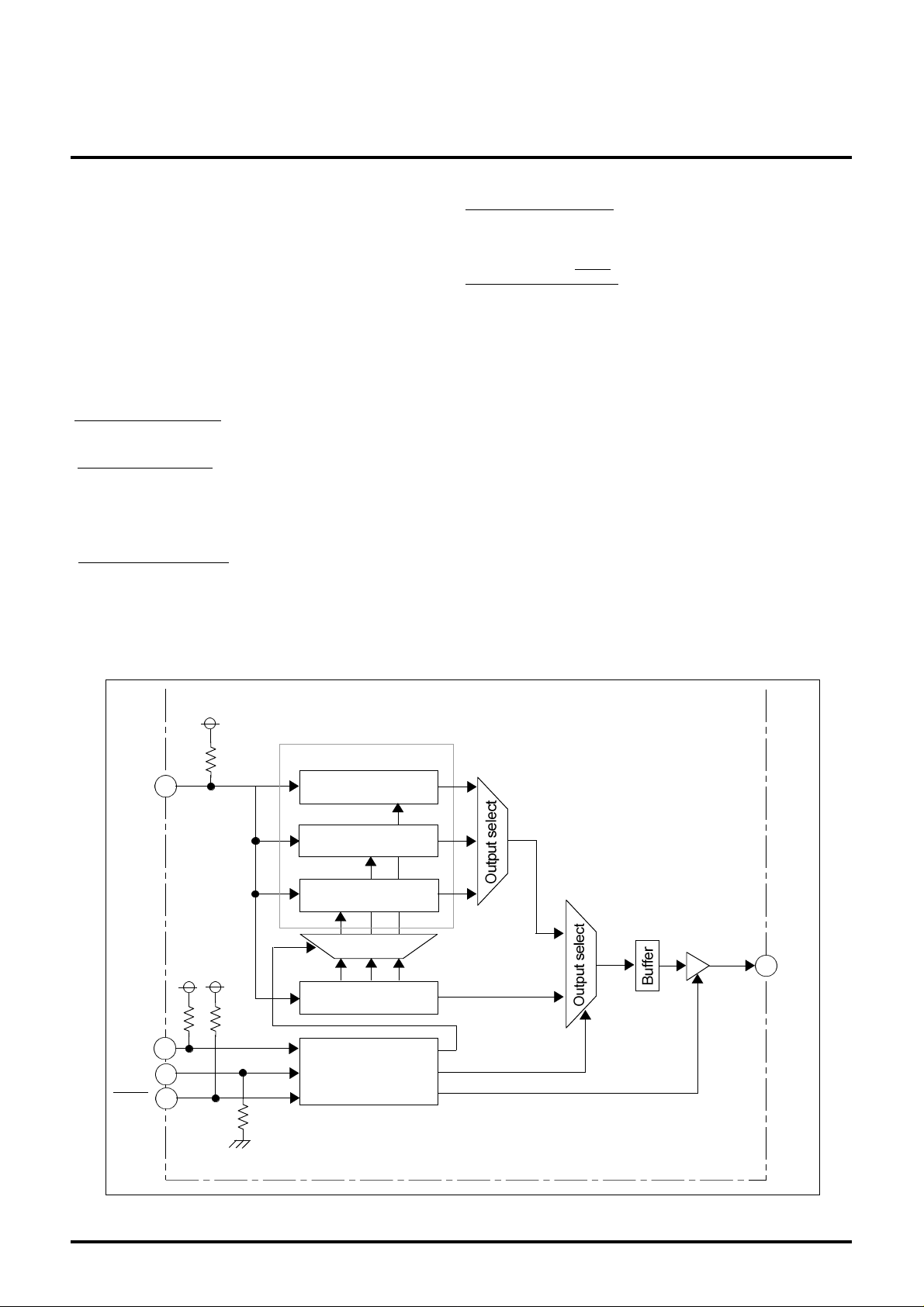
USB DEVICE CONTROLLER
Abstraction of JTAG
Pin descriptions
(4) Control logic for input select, output select, and so.
M66290A has JTAG (Joint Test Action Group) interface
which meets IEEE 1149.1 test access port spec.
This JTAG interface can be used for input/output path
(boundary scan path) for boundary scan test.
Further information as to JTAG test access port, refer
to "IEEE Std. 1149.1a-1993".
Pin description which relates to JTAG interface of
M66290A are as follows.
Test clock input (TCK)
Clock input into test circuit.
Test data input (TDI)
Synchronous serial input to input test command
code and test data. Data is sampled by the
positive edge of TCK.
Test data output (TDO)
Synchronous serial output to output test command
code and test data. Output data changes by the
negative edge of TCK and is output only in the state
of Shift-IR or Shift-DR. In other state,keeps "Z".
MITSUBISHI <DIGITAL ASSP>
M66290AGP/FP
Test mode input (TMS)
Test mode select input to control status shift of test
circuit. This is sampled by the positive edge of TCK.
Test reset input (TRST)
"L" active test reset input to initialize the test circuit
asynchronously. To assure this reset function, keep
TMS input as "H" when this signal changes from "L"
to "H".
JTAG circuit constitution
JTAG circuit of M66290A is constituted by the blocks
as follows.
(1) Command register which keeps command code
which is fetched through the boundary scan path.
(2) Data register group which is accessed through the
boundary scan pass.
(3) Test access port (TAP) controller to control the
status shift of JTAG block.
TDI
TMS
TCK
TRST
11
10
M66290A
Data register group
Boundary scan
register (JTAGBSR)
Bypass register
(JTAGBPR)
ID code register
(JTAGIDR)
Decoder
12
TDO
Command register
(3bits) (JTAGIR)
9
8
TAP controller
51
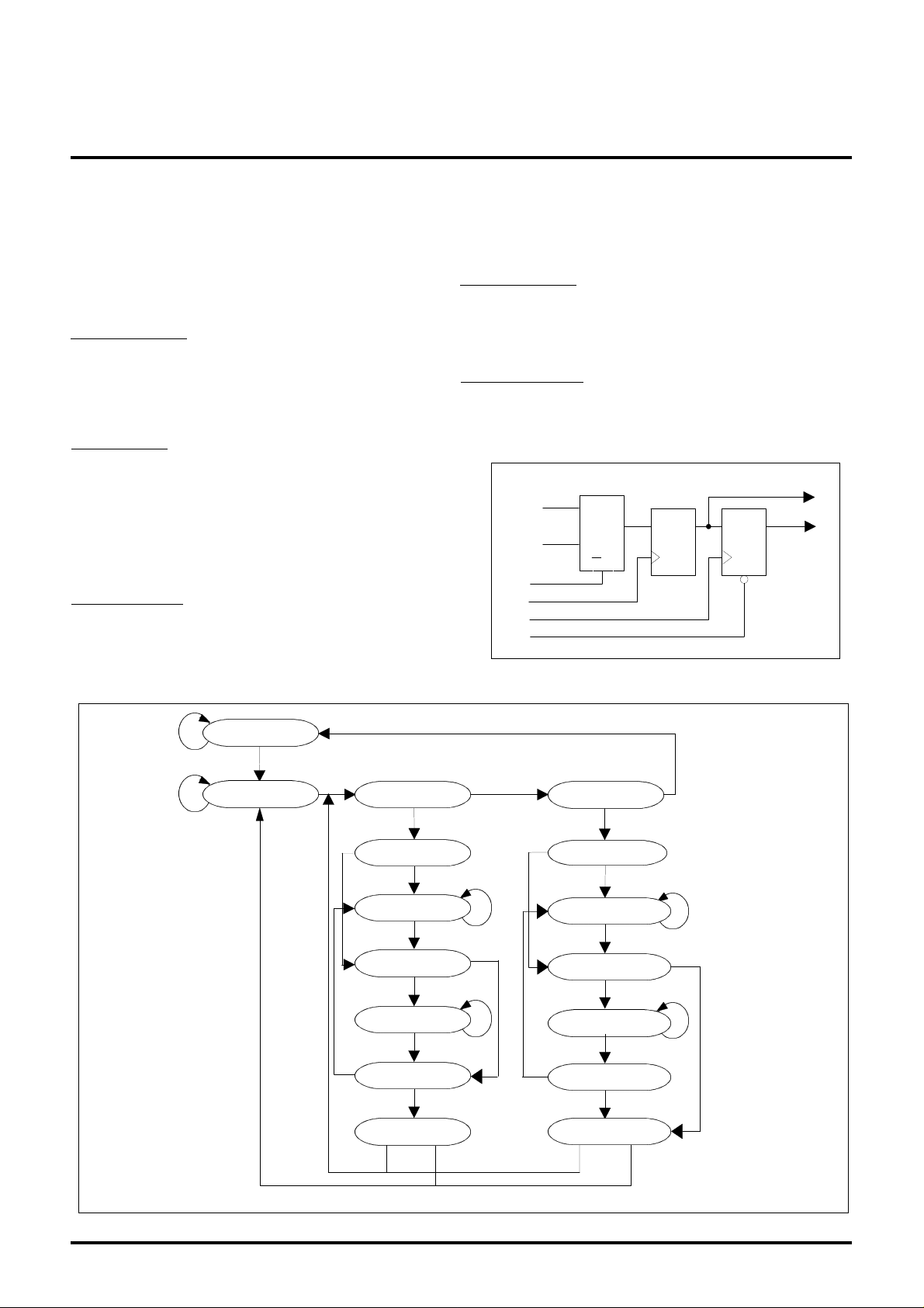
USB DEVICE CONTROLLER
MITSUBISHI <DIGITAL ASSP>
110
0
10110110100
0
0
Shift-DR/IR
Clock-DR/IR
Update-DR/IR
0
01011110100
0
Test-Logic-Reset
1
Data input
From previous
cell
Input select
Test reset
Parallel output
stage
Data output
To next cell
Shift register
stage
Abstract of JTAG operations
same time, output the data which is sampled by capture
M66290AGP/FP
There are four basic access to command register
and to data register. And the access is executed
based on the status shift of TAP controller.
TAP controller is shifted of its status by the TMS
input and make a control signal which is needed to
each state.
Capture operation
Result of the boundary scan test or the fixed
data which is defined to each register, is sampled.
For operation, load the input data into shift register
stage.
Shift operation
Through the boundary scan path, access from external
is done. M66290A set the data from external and at the
operation.
For register operation, right shift is executed among
shift register stage of each bit.
Update operation
In shift operation, drive the data which is set by external.
For register operation, transfer the value which is set to
shift register stage, to parallel output stage.
JTAG interface shifts the internal state according to TMS
input, and do two kinds of operations as follows. Both are
basically
executed in turn of "Capture -> Shift -> Update".
IR path sequence
Set the command code into command register and when
path sequence comes, select the data register which is
the object of the operation.
DR path sequence
To selected data register, refer or set the data.
A
Y
D Q
B
A/B
T
D Q
T
Figure. Basic construction of JTAG related register
Run-Test-/Idle
Figure. Status shift of TAP controller
Select-DR-Scan
Capture-DR
Shift-DR
Exit1-DR
Pause-DR
Exit2-DR
Update-DR
Select-IR-Scan
Capture-IR
Shift-IR
Exit1-IR
Pause-IR
Exit2-IR
Exit2-IR
Update-IR
note: 0,1 shows the status of TMS input signal
52

USB DEVICE CONTROLLER
JTAG registers
scan test and set into the "Boundary Scan Register"
TDO terminal, and is selected when "EXTEST Command"
the state of Capture-DR. In the state of Shift-DR, input
Command registers
Command register is constituted by 3 bits register
which keeps command code, and is set in the IR
path sequence. Data register, which is selected in
the following path sequence, is determined by the
command which is set into the command register.
Initial value in test reset is IDCODE command.
Until the command code is set from external,
IDCODE register is kept selecting as the data
register.
M66290A supports three commands (EXTEST,
SAMPLE/PRELOAD, and BYPASS) which are
established as essential by IEEE 1149.1 and the
device recognize register access command
(IDCODE).
Below are the commands and the related code.
EXTEST (Command code : b'000)
Executes outside circuit connection test and on
board connection test. Reads the TDI input into the
"Boundary Scan Register" and outputs the contents
of "Boundary Scan Register" from TDO.
MITSUBISHI <DIGITAL ASSP>
M66290AGP/FP
Data registers
(1) Boundary scan register (JTAGBSR)
This is for boundary scan test and is assigned to each
terminal of M66290A which is related to JTAG.
Boundary scan register is connected between TDI and
is ordered. This register captures the status of input
terminal or the output value from internal logic circuit in
the data for boundary scan test parallely outputting the
sampled value. And set terminal function (IN/OUT of
bidirectional terminal or direction of 3-state output) and
output value.
As to the JTAG related terminal and the structure of
boundary scan, refer to BSDL specially.
(2) BYPASS register (JTAGBPR)
BYPASS register is one bit register to bypass the boundary
scan path when M66290A is not the object in boundary scan
test. BYPASS register is connected between TDI and TDO
terminal, and is selected when "BTPASS command" is
ordered. In the state of Capture-DR, "0" is loaded.
IDCODE (Command code : b'001)
Selects the "IDCODE Register" and outputs the
device and company discrimination data from
TDO.
SAMPLE/PRELOAD (Command code : b'010)
Samples the circuit status in operation and outputs
it from TDO, and at the same time, inputs the data
from TDI which will be use in the next boundary
previously.
BYPASS (Command code : b'111)
Selects the "BYPASS Register" and executes the
refer and the set of the data.
Don't set the command code except for above.
(4) IDCODE register (JTAGIDR)
IDCODE register is a register of 32bits to discriminate the
device and the company, and keeps information as follows.
IDCODE register is connected between TDI and TDO
terminal,
and is selected when "IDCODE Command" is ordered.
IDCODE data is loaded in Capture-DR state and is output
from TDO in Shift-DR state.
1. Version information (4bits)
2. Part number (16bits)
3. Company ID (11bits)
4. LSB (1bit) : b'1
: b'0000
: b'0001 1000 1001 0010
(Binary code of "6290")
: b'000 0001 1100
(JEDEC code of MITSUBISHI)
(Fixed)
53
 Loading...