Mitsubishi M66273FP Datasheet
LCD CONTROLLER with VRAM
Ver.3.1 Dec,1999
DESCRIPTION
of up to 76800 dots(equivalent to 1/4 VGA)
Panel
Binary/
1
WAITCNT WAIT CONTROL
The M66273 is a graphic display-only controller for dot matrix type STNLCD which is used widely for OA equipment, PDA, amusement
equipment, etc.
The M66273 is an advanced product from the M66272 at the point of MPU
interface and timing specifications. This LCD display functions are the
same with the M66272.
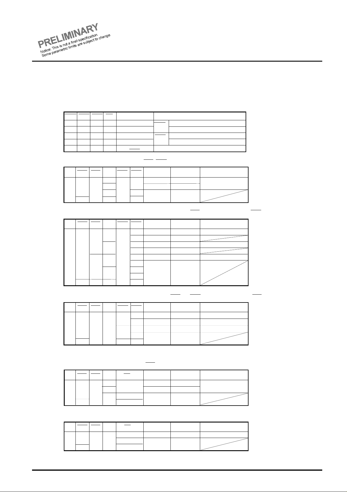
It is capable of displaying six types of LCD by combining the panel
configuration(single or dual scan), LCD display function(binary or gray
scale), LCD display data bus width(4 or 8 bit).
configuration
Single scan
Dual scan
gray scale
Binary
Gray scale
Binary
Gray scale
LCD display data
4bit
8bit
4bit
8bit
4bit
4bit
Displayable LCD size
Equivalent to 640 x 240
Equivalent to 320 x 240
Equivalent to 320 x 240 x 2 screens
Equivalent to 320 x 120 x 2 screens
The M66273 can support the reflective color type LCD (ECB : Electrically
Controlled Birefringence).
The IC has a built-in 19200-byte VRAM as a display data memory. All of
the VRAM addresses are externally opened. Direct addressing of display
data can be performed from MPU, thus display data processing such as
drawing can be efficiently carried out.
The built-in arbiter circuit(cycle steal system) which gives priority to
display access allows timing-free access from MPU to VRAM, preventing
display screen distortion.
The IC provides has a function for LCD module built-in system by
lessening connect pins between the MPU and the IC.
FEATURES
· Display memory
·Built-in 19200-byte(153.6-Kbit) VRAM(Equivalent to 640 x 240 dots x 1
screen, 320 x 240 dots x 2 screens)
· All addresses of built-in VRAM are externally opened.
MITSUBISHI <DIGITAL ASSP>
M66273FP
· Displayable LCD
· Binary display
Monochrome STN-LCD of up to 153600 dots(equivalent to 1/2
VGA)
· 4 gray scale display
Monochrome STN-LCD
Reflective color STN-LCD of up to 76800 dots (equivalent to 1/4
VGA)
· Interface with MPU
· Capability of switching the interface with two-way 8/16-bit MPU
· Provides WAIT output pin(WAIT output when access from MPU to
VRAM is gained)
· Capability of controlling BHE or LWR/HWR at the interface with a
16-bit MPU
· Interface with LCD
· LCD display data bus is a 4-bit or 8-bit parallel output.
· 4 kinds of control signals: CP, LP, FLM and M
· Display functions
· Graphic display only
· Binary or 4 gray scale display(gray scale palette is used to set
pseudo medium 2 gray scale.)
· Reflective color(ECB) uses a gray scale function.
· Vertical scrolling is allowed within memory range.
· Additional function for LCD module built-in system
· Capability of interfacing with two-way 8/16-bit MPU(16-bit MPU
byte access is not allowed.)
· Access from MPU to VRAM is gained via the I/O register.
· 5V or 3V single power supply
APPLICATION
PPC/FAX operation panel, display/operation panel of other OA
equipment, multifunction/public telephone
· PDA/electronic notebook/information terminal, portable terminal
· Game, Amusements, Kids computer, etc.
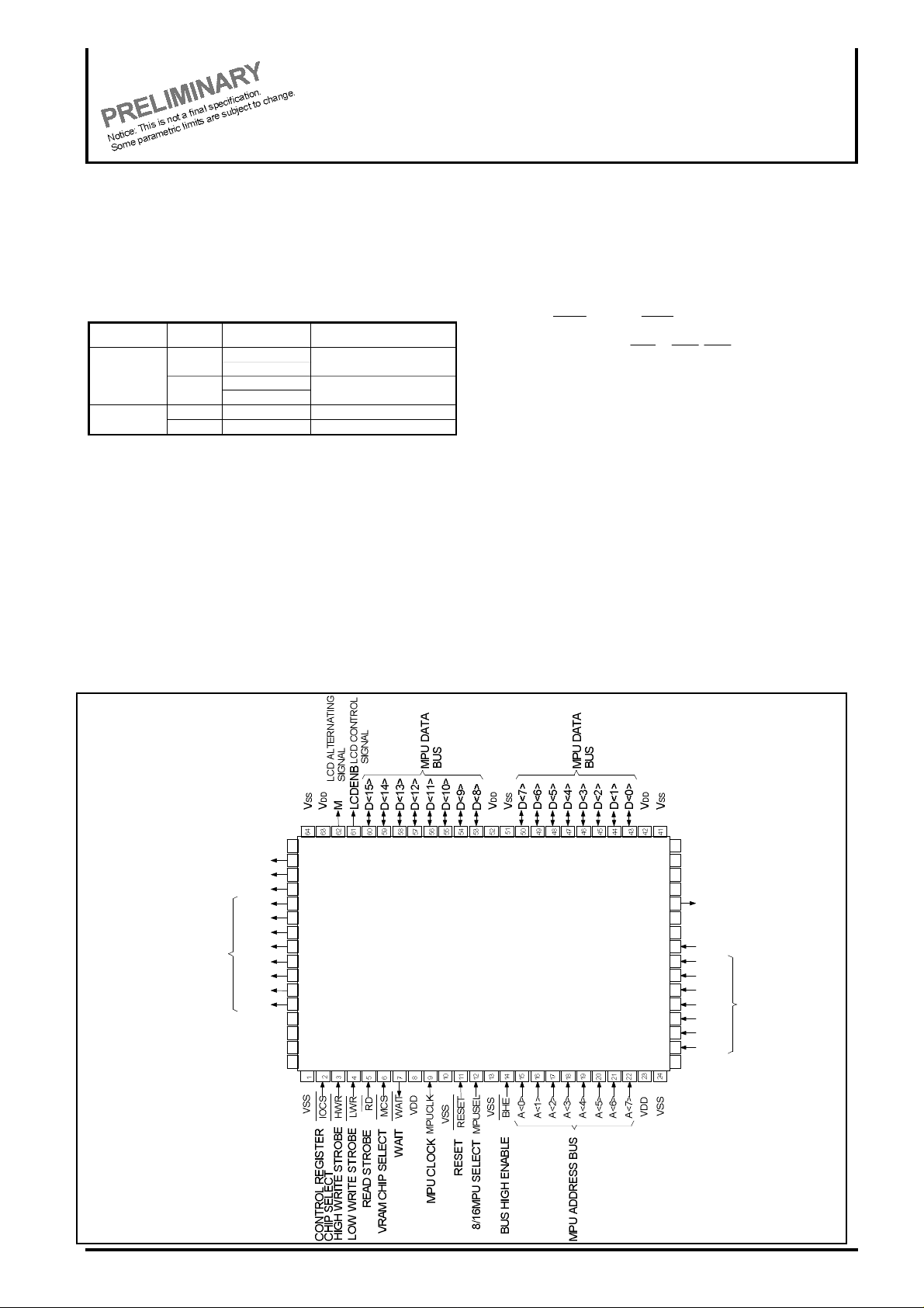
PIN CONFIGURATION
(TOP VIEW)
DISPLAY DATA TRANSFER CLOCK
DISPLAY DATA LATCH PULSE
FIRST LINE MARKER SIGNAL
LCD DISPLAY DATA BUS
VSS
CP
LP
FLM
VD<0>
VD<1>
VD<2>
VD<3>
VD<4>
VD<5>
VD<6>
VD<7>
VDD
N.C
N.C
VSS
65
66
67
68
69
70
71
72
73
74
75
76
77
78
79
80
M66273FP
40
VSS
39
N.C
38
N.C
37
N.C
36
CSE
35
VSS
34
VDD
33
32
A<14>
31
A<13>
30
A<12>
29
A<11>
28
A<10>
27
A<9>
26
A<8>
25
VSS
CYCLE STEAL
ENABLE
MPU ADDRESS
BUS
Outline 80P6N-A
N.C : No Connection
LCD CONTROLLER with VRAM
Ver.3.1 Dec,1999
MPUCLK
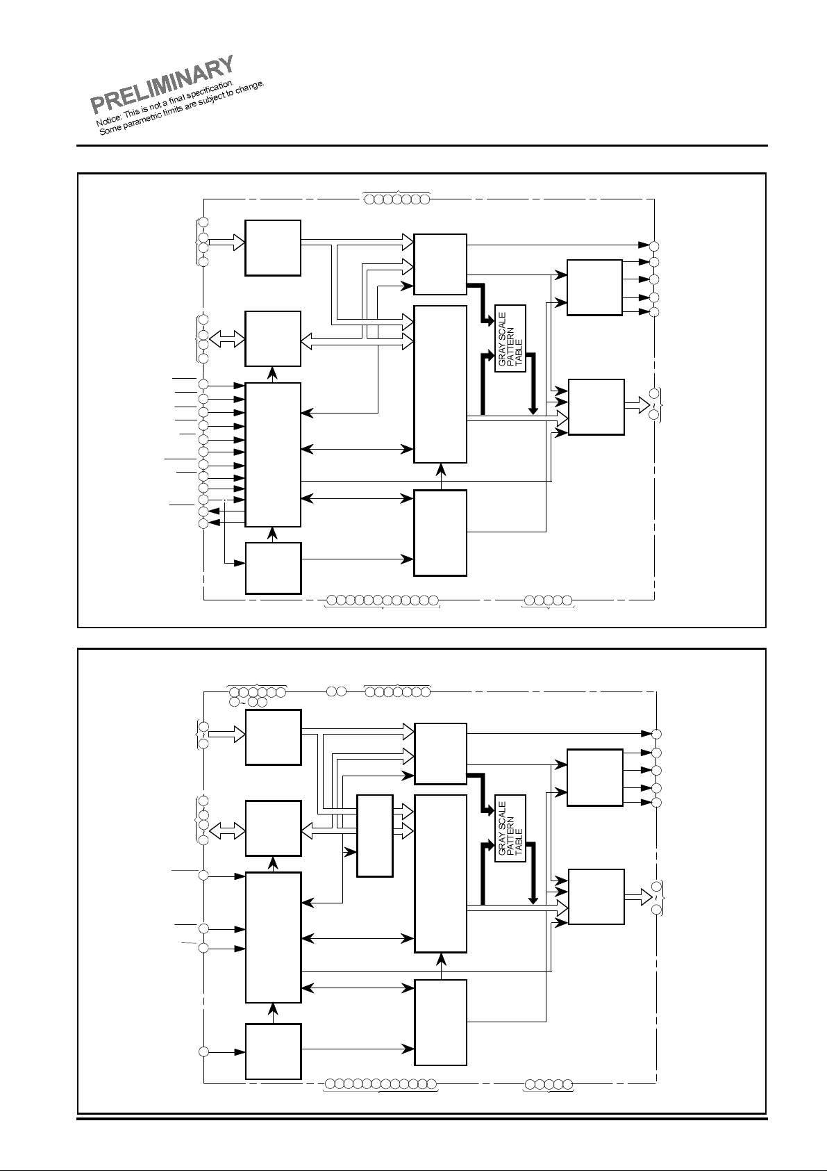
BLOCK DIAGRAM 1
A<14:0>
D<15:0>
CPLPFLMMV
LCD CONTROL
CONTROLREGISTER
V
SS
(BASIC
VRAM
A<7:1>
D<15:0>
LCDENB
V
VSSVRAM
19200byte
ADDRESS
REGISTER
REGISTER
DISPLAY DATA
DISPLAY DATA
LCD ALTERNATING
FIRST LINE MARKER
VD<7:0>
VD<7:0>
2
(CYCLE
CONTROL REGISTER
LOW WRITE STROBE
MPU ADDRESS
(BASIC
CPLPFLM
M
LCD CONTROL
SIGNAL
DISPLAY DATA
DISPLAY DATA
LCD ALTERNATING
FIRST LINE MARKER
N.C
N.C
MPU ADDRESS
BUS
MPU DATA BUS
CHIP SELECT
VRAM CHIP SELECT
HIGH WRITE STROBE
LOW WRITE STROBE
READ STROBE
8/16MPU SELECT
BUS HIGH ENABLE
MPU CLOCK
CYCLE STEAL ENABLE
MPUSEL
WAITCNTWAIT CONTROL
WAIT
RESETRESET
IOCS
MCS
HWR
LWR
RD
BHE
WAIT
CSE
MITSUBISHI <DIGITAL ASSP>
M66273FP
DD
8 233442 52 6377
15
22
26
32
43
50
53
60
2
6
3
4
5
12
11
14
33
9
7
36
ADDRESS
BUFFER
DATA
BUFFER
MPU I/F
CONTROL
CIRCUIT
CLOCK
CONTROL
TIMING
CONTROL)
CONTROL
REGISTER
19200byte
BUS
ARBITER
TIMING
CONTROL
STEAL
CONTROL)
40 41 51 64 65 80
LCDENB
61
LCD
DISPLAY
TIMING
CONTROL
CIRCUIT
LCD
DISPLAY
DATA
CONTROL
CIRCUIT
37 38 3978 791 10 13 242535
66
67
68
62
69
76
SIGNAL
TRANSFER CLOCK
LATCH PULSE
SIGNAL
SIGNAL
LCD DISPLAY
DATA BUS
BLOCK DIAGRAM 2 (When interfacing with the LCD module built-in system and having the maximum number of pins connected with MPU)
BUS
MPU DATA BUS
CHIP SELECT
READ STROBE
MPU CLOCK
IOCS
LWR
RD
MPUCLK
INPUT FIXED PIN
3 6 11 1214
26 321533
16
22
43
50
53
60
2
4
5
9
ADDRESS
BUFFER
DATA
BUFFER
MPU I/F
CONTROL
CIRCUIT
CLOCK
CONTROL
TIMING
CONTROL)
OPEN PIN
7
36
1 10 13 24 25 35 40 41 51 64 65 80
DD
8 2334 42 526377
VRAM
INDEX
DATA
PORT
CONTROL
REGISTER
BUS
ARBITER
TIMING
CONTROL
37 38 39 78 79
LCD
DISPLAY
TIMING
CONTROL
CIRCUIT
LCD
DISPLAY
DATA
CONTROL
CIRCUIT
61
66
TRANSFER CLOCK
67
LATCH PULSE
68
SIGNAL
62
SIGNAL
69
76
LCD DISPLAY
DATA BUS
LCD CONTROLLER with VRAM
Ver.3.1 Dec,1999
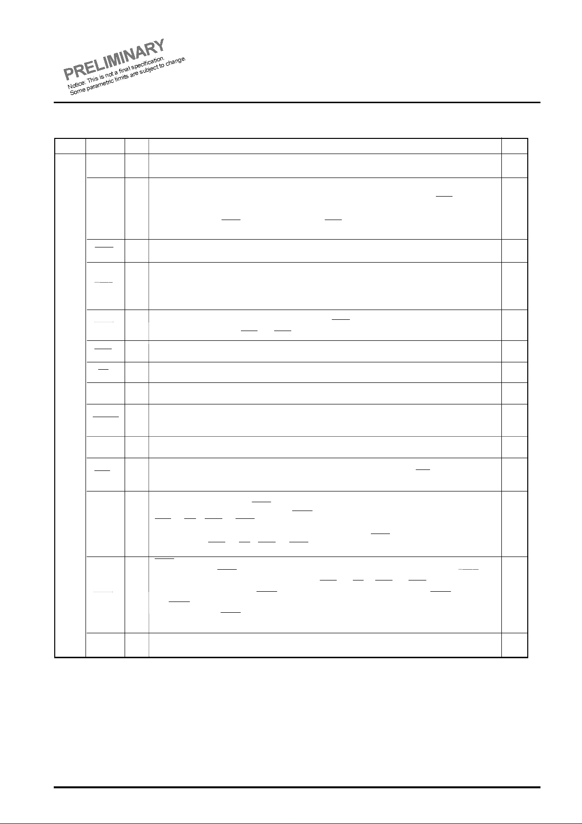
PIN DESCRIPTIONS
Input/
Output
Number
of pins
MPU address bus
is restricted. When IOCS control use A <7:0>, and MCS control use A <14:0> for selecting address of
MCS
Use this pin, when it is necessary to output WAIT earlier than the timing of falling edge of overlapping with
overlapping with MCS and RD or LWR and HWR.
3
MITSUBISHI <DIGITAL ASSP>
M66273FP
Item
MPU
interface
Pin name
D<15:0>
A<14:0>
LWR
RD
MPUSEL
RESET
MPUCLK
BHE
WAITCNT
Function
MPU data bus
Input/
When selecting 8 bit MPU by MPUSEL input, connect D<15:8> to "VDD" or "VSS".
Output
When selecting 8-bit MPU, use A<14:0>.
When selecting 16-bit MPU, use A<14:1> as a address bus. By combining A<0> and BHE, access to
internal VRAM can be gained.
Input
When driving two screens (dual scan mode), notice that the allowable setup range of VRAM address
control register.
Chip select input of control register
Input
When this pin is "L", select the internal control register. Assign to I/O space of MPU.
Chip select input of VRAM / control register
When this pin is "L", select the internal VRAM. Assign to memory space of MPU.
And this pin can for chip select of control register.
Input
In detail, refer to "COMBINATIONS OF CONTROL INPUT PINS ON THE MPU INTERFACE" and "CONTROL
REGISTER".
High-Write strobe input
When this pin is "L", write data to the internal VRAM. HWR is valid only in using 16-bit MPU
Input
controlled byte access by LWR and HWR.
Low-Write strobe input
Input
When this pin is "L", write data to the internal control register or VRAM.
Read strobe input
Input
When this pin is "L", read data from the internal control register or VRAM.
8/16-bit MPU select input
Input
According to MPU, set "VSS" for 8-bit MPU and set "VDD" for 16-bit MPU.
Reset input
Use reset signal of MPU. When this pin is "L", initialize (reset) all internal control registers and
Input
counters.
MPU clock
Input
Input system clock output from MPU.
Bus-High-Enable input
This pin is valid when using 16-bit MPU controlling byte access with A<0> and BHE.
Input
Connect to "VDD" to select 8-bit MPU.
Wait control input
This pin is used for controlling WAIT output timing when requested access from MPU to VRAM.
MCS and RD or LWR and HWR.
Input
And then connect AS, ALE or etc of MPU.
Connect WAITCNT to "VDD" or "VSS", when it is necessary to output WAIT at the timing of falling edge of
16
15
1IOCS
1
1HWR
1
1
1
1
1
1
1
WAIT output for MPU
This signal makes WAIT for MPU. In case of fixed WAITCNT input("VSS" or "VDD" )change WAIT to
"L" at the timing of falling edge of overlapping with MCS and RD or LWR and HWR. And in case of
WAIT
using WAITCNT input, change WAIT to "L" at timing of falling edge of WAITCNT on MCS = "L".
Output
And WAIT output return to "H" at synchronization with the rising edge of MPUCLK after internal
processing. (Output WAIT only when requested access from MPU to VRAM is gained during cycle
steal access.)
Cycle Steal Enable output
CSE
Output
State output of internal cycle steal access.
1
1

LCD CONTROLLER with VRAM
Ver.3.1 Dec,1999
Input/
Output
Number
of pins
mode.
Take the display data of VD<n:0> to LCD at falling edge of CP.
Latch of display data and the transfer of scanning signal at falling edge of LP.
This signal is "H" active, the IC for driving scanning line catches FLM at falling edge of LP.
4
WAITCNT input ( WAIT control input)
SWAP input ( Bus swap input)
PIN DESCRIPTIONS
MITSUBISHI <DIGITAL ASSP>
M66273FP
Item
LCD
interface
Others
Pin name
Display data bus for LCD
Transfer the LCD display data in synchronization with a rising edge of CP by putting 4-bit or 8-bit in
VD<7:0>
CP
LP
FLM
M
LCDENB
VDD
N.C No connection 10
Output
Output
Output
Output
Output
Output
parallel.
The VD<n:0> output pin in use differs depending on the number of driven screens and the display
Display data transfer clock
Shift clock for the transfer of display data to LCD.
Display data latch pulse
This clock use both as the latch pulse of display data for LCD and the transfer of scanning signal.
LP is output when it finishes transferring display data of a line.
First Line Marker signal output
Output the start pulse of scanning line.
LCD alternating signal output
Signal for driving LCD by alternating current.
LCD (ON/OFF) control signal output
Output data which is set at bit "0" of mode register (R1) in the control register. This signal can be used
for controlling the LCD power supply, because LCDENB is set to "L" by RESET.
Power supply pin
Function
7
8
1
1
1
1
1
7VSS Ground
DIFFERENCE BETWEEN M66273FP AND M66272FP
The M66273FP is an advanced product from the M66272FP at the point of MPU interface and timing
specifications.
LCD display functions are the same with the M66272FP.
The following shows difference between the M66273FP and the M66272FP without timing specifications.
Refer to the later item about timing specifications and detail specifications.
Specification
Pin function
WAIT output
control
Access to
control register
Bus swap function
M66273FP
It is capable of selecting WAIT output trigger input.
In case of fixed WAITCNT input, change WAIT to "L" at the
timing of the falling edge of overlapping with MCS and RD or
LWR/HWR, and in case of using WAITCNT input, change
WAIT to "L" at the timing of the falling edge of WAITCNT on
MCS="L".
Use IOCS or MCS pins for chip select of
control register.
(capable of controlling VRAM and control register by MCS
pin.)
Set by SWAP register.
M66272FP
WAIT output change to "L" at the timing of the falling
edge of overlapping with MCS and RD or LWR/HWR.
Use IOCS pin for chip select of control register.
Set by SWAP pin.
LCD CONTROLLER with VRAM
Ver.3.1 Dec,1999
M output is an LCD alternating signal for driving LCD with alternating
OUTLINE
gray scale
size
mode
12345
6
32456
5
1
MITSUBISHI <DIGITAL ASSP>
M66273FP
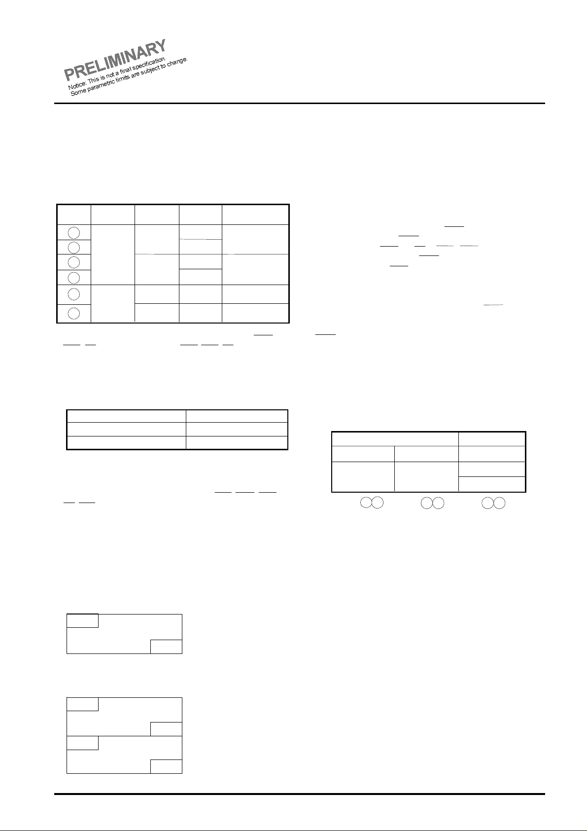
The M66273 is a graphic display only controller for displaying a dot
matrix type STN-LCD.
· LCD display mode
It is capable of displaying six types of LCD by combining the panel
configuration, binary/gray scale, LCD display data bus width.
Display
· Control register
Refer to Table-1, setting of control input.
· VRAM
Refer to table-2 to 6, VRAM specifications for 8/16 bit MPU and input
Panel
configuration
Single
scan
Dual
scan
When accessing the control register from MPU, use pins IOCS,
LWR, RD, A<7:0> and D<7:0>, or MCS, LWR, RD,A<14:0> and
D<7:0> (However, use D<15:0> only when 16-bit MPU controls the
LCD module built-in support function.)
The IC contains the following registers as control registers.
Operation control
Supporting LCD module built-in type
Gray scale pattern table
This IC has a built-in 19200-byte VRAM which is equivalent to two
screens of 320 x 240 dots LCD.
When accessing VRAM from MPU, use pins MCS, HWR, LWR,
RD, BHE, A<14:0> and D<15:0>.
Use of MPUSEL input can support both 8/16 bit MPU.
setting in access.
The VRAM address settable range is restricted depending on the
panel configuration, as follows.
Binary/
Binary
Gray scale
Binary
Gray scale
LCD display
data
4bit
8bit
4bit
8bit
4bit
4bit
R1 to R11
R12 to 14 or R15 to 16
R17 to R80
Displayable LCD
Equivalent to 640
x 240
Equivalent to 320
x 240
Equivalent to 320 x
240 x 2 screens
Equivalent to 320 x
120 x 2 screens
· Cycle steal system
Cycle steal system is interact method of transforming display data for
LCD from VRAM and accessing VRAM from MPU on the basic
cycle (MAINCLK) of internal operation.
Basic timing is two clocks of MAINCLK, and assign first clock to the
access from MPU to VRAM and second clock to the transfer of
display data from VRAM to LCD.
In accessing VRAM from MPU, output WAIT. In case of fixed
WAITCNT input, change WAIT to "L" at the timing of the falling edge
of overlapping with MCS and RD or LWR / HWR,and in case of
using WAITCNT input, change WAIT to "L" at the timing of the falling
edge of WAITCNT on MCS="L", And return to "H" at synchronizing
with rising edge of MPUCLK after internal processing.
For the cycle steal system, this IC provides a cycle steal control
function to improve data transfer efficiency in a line. This func-tion
gains access with the cycle steal system by taking WAIT for MPU
during the display term with necessity for the display data transfer
from built-in VRAM to LCD. On the other side, it does not output
WAIT for keeping throughput of MPU during horizontal synchronous
term (idle running term) with no necessity for the display data
transfer from VRAM to LCD side.
In detail,refer to "Description of cycle steal".
· Output to LCD side
LCD display data VD<7:0> is output in parallel per 4 bits or 8 bits in
synchronization with the rising edge of CP.
Pin VD<n:0> differs depending on the display mode.
Single scan
4-bit transfer
VD<3:0> VD<7:0> VD<3:0>
Display mode
When display data for a line has been sent, LP outputs data in
synchronization with the falling edge of MAINCLK.
The IC enables adjustment to an optimum value of the frame
frequency as requested from the LCD PANEL side by adjusting pulse
width of LP with the LPW register value.
FLM is output when the display data for the first line has been sent.
8-bit transfer 4-bit transfer
Dual scan
VD<7:4>
VRAM address settable range
· When single scan mode
·A<14:0>=0000 to 4AFFH --- 19200 byte
0000H
VRAM
4AFFH
· When dual scan mode
·For the 1st screen --- A<14:0>=0000 to 257FH --- 9600 byte
·For the 2nd screen --- A<14:0>=2580 to 4AFFH --- 9600 byte
0000H
VRAM for the 1st screen
257FH
2580H
VRAM for the 2nd screen
4AFFH
current.
M output cycles can be set in lines with the M output cycle variable
register and is available to prevent LCD from deterioration.
· Gray scale display function
Gray scale display can assign 2-bit VRAM data to a picture element
of LCD display to show the display density at four levels.
Gray scale display pattern tables 0 and 1 (4 x 4 matrix x 16 patterns x
2 medium gray scale), consisting of SRAM of 64 bytes in total, can
set any gray scale display pattern.
In detail,refer to "Description of gray scale function".
· Application to reflective color type LCD
The above gradation display function is available to control about four
display colors on the reflective color type LCD with ECB (Electrically
Controlled Birefringence).
LCD CONTROLLER with VRAM
MITSUBISHI <DIGITAL ASSP>
6
Ver.3.1 Dec,1999
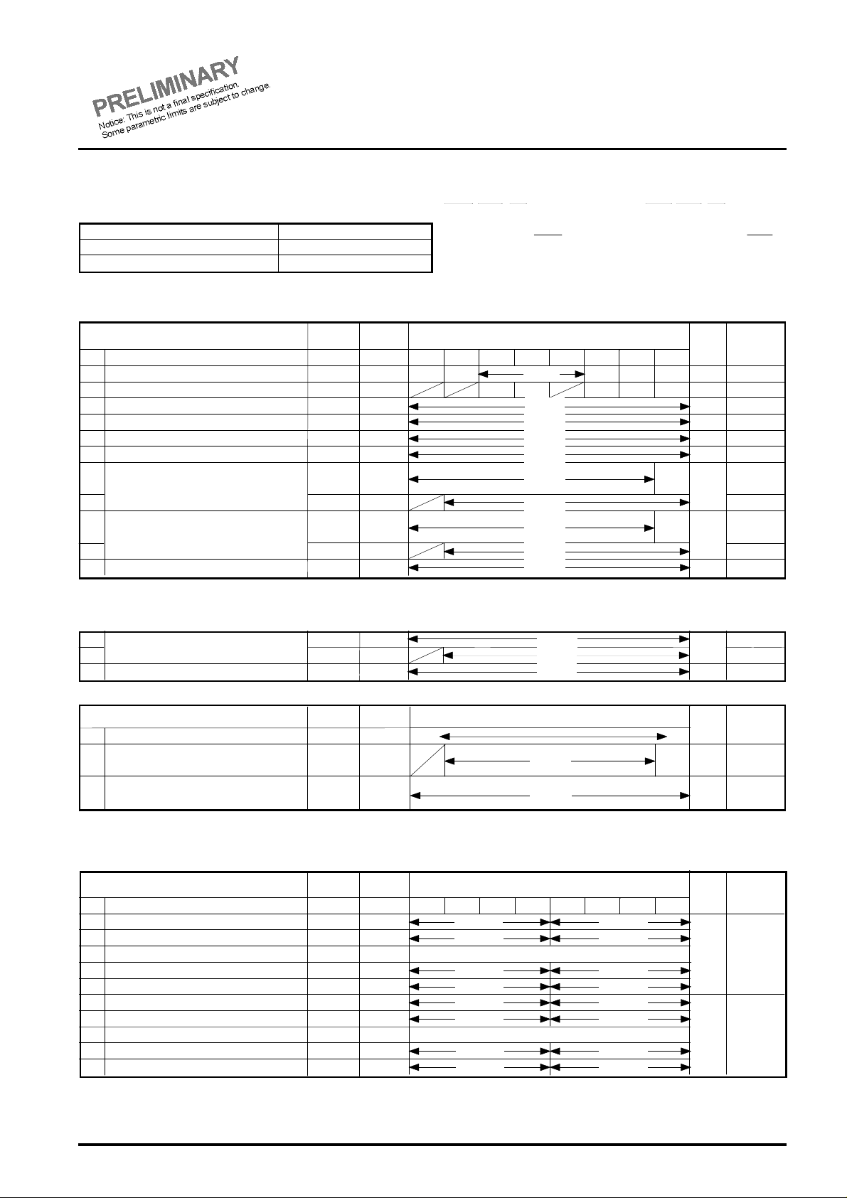
COMBINATIONS OF CONTROL INPUT PINS ON THE MPU INTERFACE
Tables 1 to 6 show input setting conditions for access to the control register and VRAM from the MPU side.
(1) Access to the control register
For data, D<7:0> is used.
(Only when 16bit MPU is used to control the LCD module built-in system, D<15:0> is used for data.)
Table-1
MCS
L H
L H
H L
HHL
A<14:0>
L
H
0000H to 009EH
H
L
0000H to 009EH
L
H
5000H to 509EH
H
L
5000H to 509EH
H
X
X
IOCS
control
MCS
control
(2) Write to VRAM
(2-1) For use of 8bit MPU (Set as follow: MPUSEL="L", BHE=HWR="H")
Table-2
MPU
SEL
L H L
L
H L
H
A<0>BHEMCS HWR LWR
H
X H
X
X
Odd address
Invalid Write
Write Invalid
Invalid Invalid
Even address
OperationIOCS LWR RD
Writes to control register
Reads from control register
Writes to control register
Reads from control register
Invalid
Valid data bus width
for MPU
8bit
M66273FP
(2-2) For use of 16bit MPU - 1 (For MPU controlling byte access with A<0> and BHE, set as follow: MPUSEL=HWR="H")
Table-3
MPU
SEL
A<0>BHEMCS HWR LWR
LLLH
H
L
H
H
XXH
H L
Upper byte Lower byte
Write
H
Invalid
Write Invalid
L
H
Invalid Invalid
Invalid Write
L
H
L
Invalid
H
X
Write
Invalid
Invalid
Valid data bus width
for MPU
16bit
Upper 8bit
Lower 8bit
(2-3) For use of 16bit MPU - 2 (For MPU controlling byte access with LWR and HWR, set as follow: MPUSEL=BHE="H", A<0>="L")
Table-4
MPU
SEL
A<0>
BHEMCS HWR LWR
H
L LLHLH
H
X X
H
L
H
Upper byte
Write
Write
Invalid
Invalid
Lower byte
Write
Invalid
Write
Invalid
Valid data bus width
for MPU
16bit
Upper 8bit
Lower 8bit
(3) Read from VRAM
(3-1) For use of 8bit MPU (Set as follows: MPUSEL="L", BHE="H")
Table-5
MPU
SEL
L
MCS
L
H
BHE
H
A<0>
L
H
X
RD
L Read
Odd address
Invalid
Read
H
X
Invalid Invalid
Even address
Invalid
Valid data bus width
for MPU
8bit
(3-2) For use of 16bit MPU (Set as follow: MPUSEL="H")
Table-6
MPU
SEL
H
Notes : Combinations except for the above cause malfunction. Be sure to make settings according to the above combinations.
: X=either "L" or "H"
MCS
H
BHE
A<0> RD
L
H
X
Upper byte
Read
Invalid
Lower byte
Read
Invalid
Valid data bus width
for MPU
16bitL X X
LCD CONTROLLER with VRAM
MITSUBISHI <DIGITAL ASSP>
CONTROL REGISTER
LCDE
REV
DISP
DIV
IDXON
RESET
GRAY
DUAL
FRC0-1-4
FRC0-16-2
FRC1-1-4
FRC0-1-3
FRC0-16-1
FRC1-1-1
FRC1-1-3
7
WAITC
SWAP
(ICOS control)
M66273FP
Ver.3.1 Dec,1999
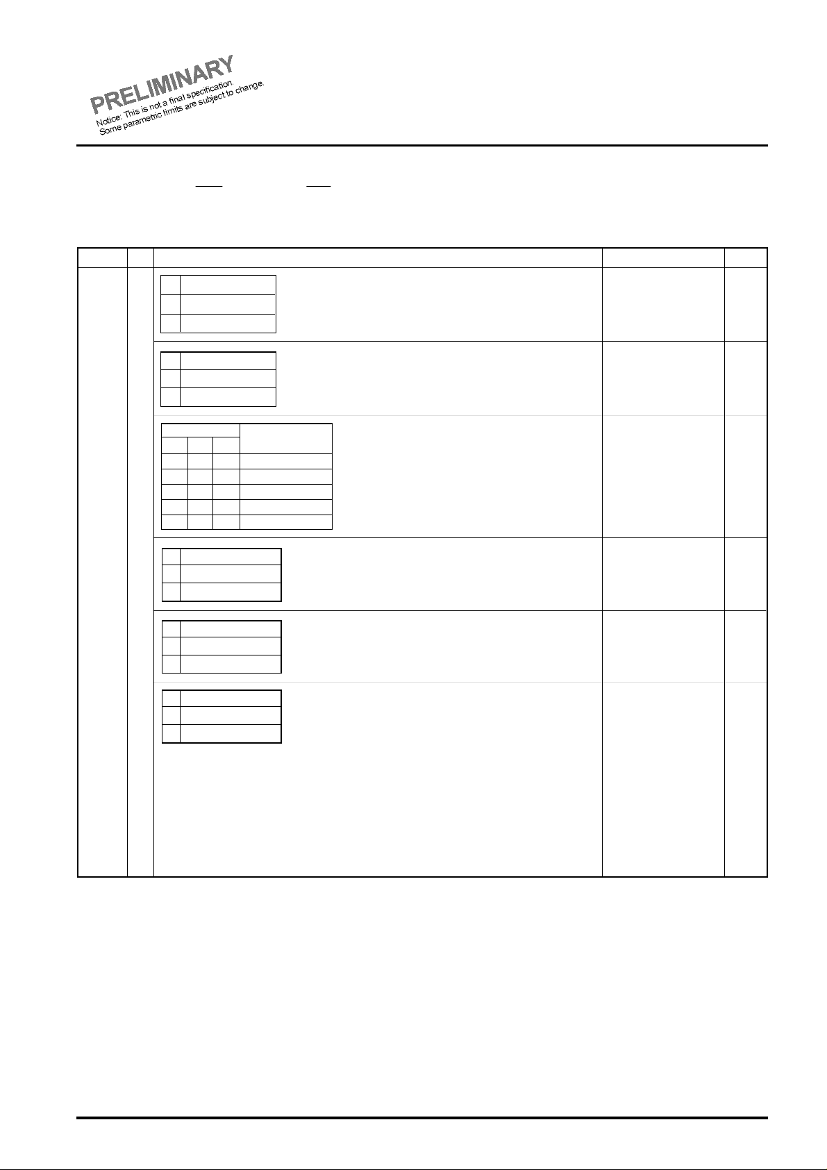
M66273 is equipped with 80 types of built-in control registers. IOCS, LWR, RD, A<7:0> and D<7:0>, or MCS, LWR, RD, A<14:0>
For operation control
Only for LCD module built-in system
For gradation pattern table
R1 to R11
R12 to R14, or R15 to R17
R17 to R80
(1) Types of control registers
· List of registers for operation control
Types of register
No. D0D1D3D4D5
R1
Basic operation mode
R2
LCD output mode
Number of horizontal display characters
R3
Horizontal synchronous pulse width
R4
Cycle steal enable width
R5
Number of vertical lines
R6
R7
1st screen display start address
Name
Address
(ICOS control)
A<7:0>
R8
R9
2nd screen display start address
R10
M output frequency variable
R11
00H
02H
04H
06H
08H
0AH
0CH
0EH
10H
12H
14H
Address
(MCS control)
A<14:0>
5000H
5002H
5004H
5006H
5008H
500AH
500CH
500EH
5010H
5012H
5014H
and D<7:0> are used for setting from the MPU to control register.
And for address in IOCS control,use A<7:0>=00H to 9EH,and in MCS
control, use A<14:0>=5000H to 509EH.
(However, D<15:0> is to be used only when registers R15 and R16
only for LCD module built-in system are used.)
Data
R/W
Reset
D2D6D7
00H
00H
W
28H
04H
W
02H
W
78H
W
00H
00H
80H
25H
00H
W
CR
LPW
CSW
SLT
SA1L
SA1H
SA2L
SA2H
MT
4/8
D0
0
D0
0
R/W
R/W
R/W
R/W
· List of registers only for LCD module built-in type support function
(For 8bit MPU only)
R12
VRAM address index
R13
R14 Data port
16H
18H
1AH
5016H
5018H
501AH
IDX8L
IDX8H
DP8
(For 16bit MPU only)
Types of register
No.
R15
VRAM address index
R16
Data port
Name
Address
A<7:0>
1CH
1EH
Address
(ICOS control)
A<14:0>
501CH
501EH
Data
D15
D14 D1
D15
IDX16
DP16
· List of registers for gray scale pattern table
Types of register
No. D0D1D3D4D5
R17
Gray scale pattern 0-1
R18
Gray scale pattern 0-2
Name
Address
(ICOS control)
A<7:0>
20H
22H
Address
(ICOS control9
A<14:0>
5020H
5022H
Data
FRC0-1-2
to to to to to to
R47
Gray scale pattern 0-31
Gray scale pattern 0-32
R48
R49
Gray scale pattern 1-1
R50
Gray scale pattern 1-2
5CH
5EH
60H
62H
505CH
505EH
5060H
5062H
FRC0-16-4
FRC1-1-2
to to to to to to
R79
Gray scale pattern 1-31
R80
Gray scale pattern 1-32
9CH
9EH
509CH
509EH
FRC1-16-2
FRC1-16-4
D2D6D7
FRC0-1-1
FRC0-16-3
FRC1-16-1
FRC1-16-3
D0
0
D0
D0
R/W
R/W
R/W
R/W
R/W
R/W
R/W
R/W
00H
00H
Undetermined
Reset
0000H
Undetermined
Reset
Undetermined
Undetermined
LCD CONTROLLER with VRAM
Ver.3.1 Dec,1999
Don't set except for the
settings in the table at
8
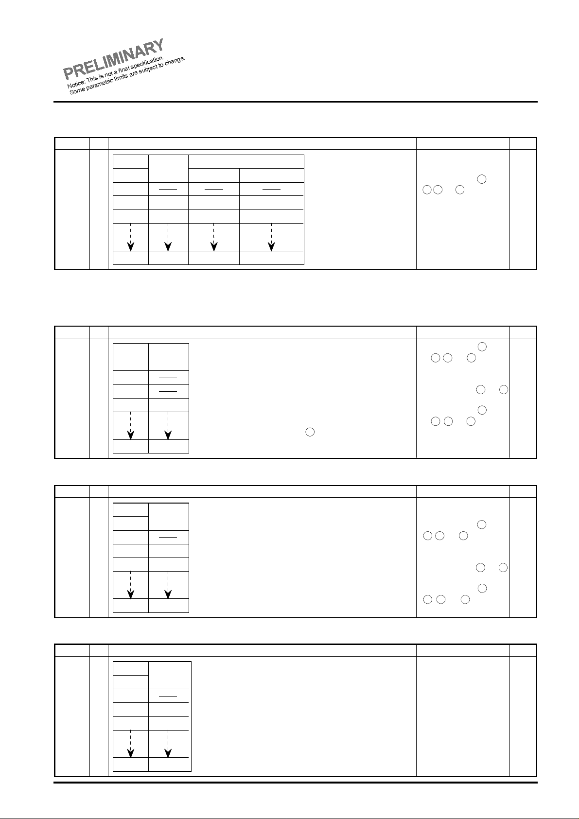
(2) Description of registers
Address is listed for ICOS control. Incase of MCS control,set to address adding 50H to upper 7 bit (50**H).
[R1] Basic operation mode
Set the Basic operation mode
Address
R/W
D7
01Reset OFF
RESET
Reset ON
·Software reset.
Function
MITSUBISHI <DIGITAL ASSP>
M66273FP
Restriction
·Surely return to reset
off after reset on.
And then, can't set
another bits (D6 to
D0) at the same time.
Reset
0
00H
D6
0
1
D5 D4 D3
R/W
D2
01Display OFF
D1
01Normal display
D0
0
1
IDXON
Index mode OFF
Index mode ON
DIV
0 0 0
0 0 1
0 1 0
0 1 1
1 0 0
DISP
Display ON
REV
Reverse display
LCDE
LCDENB="0"output
LCDENB="1"output
·Set to decide whether or not the function only for LCD
module built-in system is used.
·Set Index mode OFF for reset.
Division of
MPUCLK input
1
1/2 division
1/4 division
1/8 division
1/16 division
·Control display ON/OFF of LCD.
·In the reverse mode with REV (D1) set to "1", "1" is output to
display data VD<n:0> with DISP="0".
·Reset sets display OFF.
·Controls normal/reverse of LCD display.
·Resetting sets normal display.
·Sets the data output from the LCDENB output pin.
·Resetting outputs "0" (Vss potential) to the LCDENB output pin.
·This function is prepared for controlling the apply voltage to LCD.
When the power supply is turned ON after registers have been
completely set, set this LCDE to "1" to apply the LCD voltage.
Conversely for turning OFF the power supply to the system, set
the LCDE to "0" to turn OFF the LCD voltage.
This prevents abnormal DC voltage from being applied to the
LCD.
This function depends on the LCD functions.
Use the function, if necessary.
·Set the division of MPUCLK input to set the
reference clock cycle (MAINCLK) for internal
operation.
·Resetting does not divide MPUCLK.
0
·
left.
000
0
0
0

LCD CONTROLLER with VRAM
Ver.3.1 Dec,1999
MCS and RD or H/LWR
·When setting WAITC to "0", change WAIT to "L" at timing of
·When setting WAITC to "T", change WAIT to "L" at timing of
9
Order of upper/lower byte
Even if setting to "1", use D<7:0> to access to register of
[R2] MPUI/LCD mode
Set the display data output mode on the LCD side.
Address Function
R/W
D7 , D6 are not used.
D5
0
control
WAITCNT control
1
WAITC
·To read R2, "0" is output to D7 , D6.
·Set to select trigger signal of WAIT output.
falling edge of overlapping with MCS and RD or LWR and
HWR. And return to "H" at synchronization with the rising
edge of MPUCLK offer internal processing.
falling edge of WAITCNT on MCS="L".And return to "H" at
synchronization with rising edge of MPUCLK after internal
processing.
·Output WAIT only when requested access from MPU to
VRAM is gained during cycle steal access.
·Resetting set WAITC ="0".
MITSUBISHI <DIGITAL ASSP>
M66273FP
Restriction
·set when register is
initialized.
·When setting to
"0",connect
WAITCNT input to
VSS or VDD.
Reset
0
0
D4
R/W02H
0
1
Order of lower/upper byte
D3 is not used.
D2
1 screen driving panel
0
2 screen driving panel
1
D1
01Binary display mode
Gray scale display mode
0
1
SWAP
DUAL
GRAY
4/8D0
4bit transfer
8bit transfer
·When selecting 16 bit MPU, set SWAP to "0" to transfer
VD<n:0> in order of Upper/Lower byte of MPU data
bus,reversally set to "1" in order of Lower/Upper byte.
·When selecting 8 bit MPU, set to "0"
·
8 bit width.
·Resetting set SWAP="0".
·To read R2, "0" is output to D3.
·Set the LCD panel configuration.
·Resetting sets the 1 screen driving panel.
·Set the LCD display mode (binary or gray scale).
·Resetting sets the binary display mode.
·Set the transfer path width of the LCD display data path
VD<n:0>.
·Resetting sets 4bit transfer.
·set when register is
initialized.
·set when register is
initialized.
·set when register is
initialized.
·set when register is
initialized.
0
0
0
0
0
LCD CONTROLLER with VRAM
MITSUBISHI <DIGITAL ASSP>
In display modes and
cording to the number of
10
M66273FP
Ver.3.1 Dec,1999
[R3] Number of horizontal display characters
Address Function Reset
R/W
W04H
CR
D7 to D0
00H
01H
02H
Number of
characters
1
2
Number of LCD display dots
Binary display
Gray scale display
8
16
·Sets the number of hori-zontal
display characters per line.
·Resetting sets "28H" (=40
characters).
4
8
Restriction
·For CR, maximum of 255
characters can be set.
·In display modes ,
3 4 6
, and , the number
2
of even cha-racters can be
set.
28H
FFH
(Note) Definition of the number of characters
The number of display characters means data corresponding to 1byte of VRAM.
One character : In the case of binary, one character means 8dots of LCD display.
In the case of gray scale display, one character means 4dots of LCD display (because 2bits of VRAM corresponds to 1dot of LCD display).
255
2040
1020
[R4] Horizontal synchronous pulse width
Address Function Reset
R/W
W06H
LPW
D7 to D0
00H
01H
02H
Number of
characters
2
·In the unit of characters, set the width of horizontal synchronous
pulse generated per line.
Horizontal synchronous pulse is output from the LP pin and is
used for serial/parallel conversion of displayed data.
Adjustment of LPW can set the frame frequency to an optimum
value.
The LP output pulse actually generated takes the value(LPW
setup value - 2CP), taking into account the CP output timing.
4
FFH
255
Only in the case of display mode , however, the LP output
pulse takes the value (LPW set value - 1CP).
·Resetting sets "04H" (= 4 characters).
Restriction
·In display modes
3 4 6
, , and , only the
2
number of even characters
can be set.
·In display modes and
1 5
, set LPW to 02H or more.
·In display modes
3 4 6
, , and , set LPW
2
to 04H or more.
[R5] Cycle steal enable width
Address Function Reset
R/W
W08H
CSW
D7 to D0
00H
01H
02H
FFH
Number of
characters
1
2
255
·In unit of characters, set the period of access by the cycle steal
system near the end of the horizontal synchronous portion set
with LPW.
·With CSW=LPW, gain access by the permanent cycle steal
system.
·Resetting sets "02H" (=2 characters).
Restriction
·Set CSW to the LPW set
value or less.
·In display modes ,
3 4 6
, and , only the
2
number of even
characters can be set.
·
1 5
,set CSW to 01H or more.
·In display modes ,
3 4 6
, and , set CSW
2
to 02H or more.
04H
02H
[R6] Number of vertical lines
Address Function Reset
R/W
W0AH
SLT
D7 to D0
00H
01H
02H
FFH
Number of
vertical lines
2
4
510
·Sets the number of lines displayed in the direction of LCD vertical
line.
·SLT also sets the LCD display driving duty.
·In dual scan mode, the actual number of displayed lines is given
by SLT x 2 screens.
·Resetting sets "78H" (=240 lines).
Restriction
·Be sure to set SLT ac-
LCD display lines.
·For SLT, a maximum of
510 even lines can be
set.
78H
LCD CONTROLLER with VRAM
Ver.3.1 Dec,1999
(SA1L)
At the display start add-ress,
(SA1H)
(SA2L)
(SA2H)
11
[R7, R8] 1st screen display start address
Address
0CH
0EH
R/W
R/W
D7
SA1H
D6 to D0
00H
00H
00H
4AH
SA1L
D7 to D0
00H
02H
04H
FEH
1st screen display start
address
Function
0000H
0002H
0004H
4AFEH
MITSUBISHI <DIGITAL ASSP>
·Sets the 1st screen display
start address.
·The display start address is
determined by writing data
into SA1H.
·Reading SA1H outputs "0" to
D7.
·Resetting sets "0000H".
M66273FP
Restriction
·
even addresses can only
be set.
· For single scan;
0000H to 4AFEH
· For dual scan;
Sets 0000H to 257EH.
Settings except for the
above must not be made.
·To modify the display start
address, be sure to
respecify in order of SA1LSA1H even when only
SA1L is modified.
Reset
00H
00H
[R9, R10] 2nd screen display start address
Address
10H
12H
R/W
R/W
D7
SA2H
D6 to D0
25H
25H
25H
4AH
SA2L
D7 to D0
80H
82H
84H
FEH
2nd screen display start
address
[R11] M output cycle variable
Address
14H
R/W
W
MT
D7 to D0
00H
01H
02H
FFH
Output cycle of M signal
Makes toggle change every frame.
Makes toggle change every line (=1LP).
Makes toggle change every 2 lines.
Makes toggle change every 255 lines.
Function
2580H
2582H
2584H
4AFEH
Function
·Used for dual scan mode
only to set the 2nd
screen display start
address.
·The display start address is
determined by writing data
into SA2H.
·Reading SA2H outputs "0" to
D7.
·Resetting sets "2580H".
·Sets the output cycle of M signal
output from the M terminal.
With MT=01H, for example, M sig-
nal repeatedly reverses (toggles)
every line.
·Resetting sets "00H".
·It is recommended to set this
register to an optimum value according to the LCD specification.
Restriction
·At the display start address, only even addresses can be set, and;
·Can set 2580H to 4AFEH.
Settings except for the
above must not be
made.
·To modify the display start
address, be sure to
respecify in order of
SA2L - SA2H even when
only SA2L is modified.
Restriction
Reset
80H
25H
Reset
00H
 Loading...