Mitsubishi M66271FP Datasheet
MITSUBISHI <DIGITAL ASSP>
M66271FP
OPERATION PANEL CONTROLLER
DESCRIPTION
The M66271FP is a graphic display-only controller for displaying a
high duty dot matrix type LCD which is used widely for PPC,FAX
and multi-function telephones.
It is capable of controlling a monochrome STN LCD system of up
to 320 x 240 dots.
The IC has a built-in 9600-byte VRAM as a display data memory.
All of the VRAM addresses are externally opened. Address
mapping in the MPU memory space allows direct addressing of all
display data from the MPU,thus providing efficient display data
processing such as drawing.
The built-in arbiter circuit (cycle steal system) which gives priority
to display access allows timing-free access from MPU to VRAM,
preventing display screen distortion.
The IC provides interface with a 8-bit/16-bit MPU with a
READY(WAIT) pin.
And this IC has a function for LCD module built-in system by
lessening connect pins between MPU.
FEATURES
●Displayable LCD
•Monochrome STN dot matrix type LCD of up to 76800
dots (equivalent to 320 × 240 dots)
•Maximum display duty : 1/240 (set to 240 Line)
: 1/255 (Max)
●Display memory
•Built-in 9600-byte(76800-bit)VRAM (equivalent to one
screen of 320 × 240 dots LCD)
•All addresses of built-in VRAM are externally opened.
●Interface with MPU
•Capability of switching 8-bit type MPU/16-bit type MPU
•With WAIT output pin (Accessing register from MPU without
WAIT output. Accessing VRAM from MPU with WAIT output.)
•Capability of controlling BHE or LWR/ HWR at the interface
with a 16-bit MPU.
●Interface with LCD
•LCD display data are 4-bit parallel output
•4 kinds of control signals: CP,LP,FLM and M
●Display functions
•Graphic display only (characters drawn graphically)
•Binary display only (without tone display function)
•Vertical scrolling is allowed within memory range
(small size LCD only)
●Additional function for LCD module built-in system
•15 kinds of interface with MPU : A<4:1>,D<7:0>,IOCS,
•Accessing VRAM from MPU through I/O register
•Capability of interfacing with 8-bit type MPU only
LW R
●5V single power supply
●80-pin QFP
APPLICATION
•PPC/FAX operation panel,display/operation panel of other OA
equipment
•Multi-function/public telephones
•PDA/electronic notebook/information terminal
•Other applications using LCD of 76800 dots or less
,RD
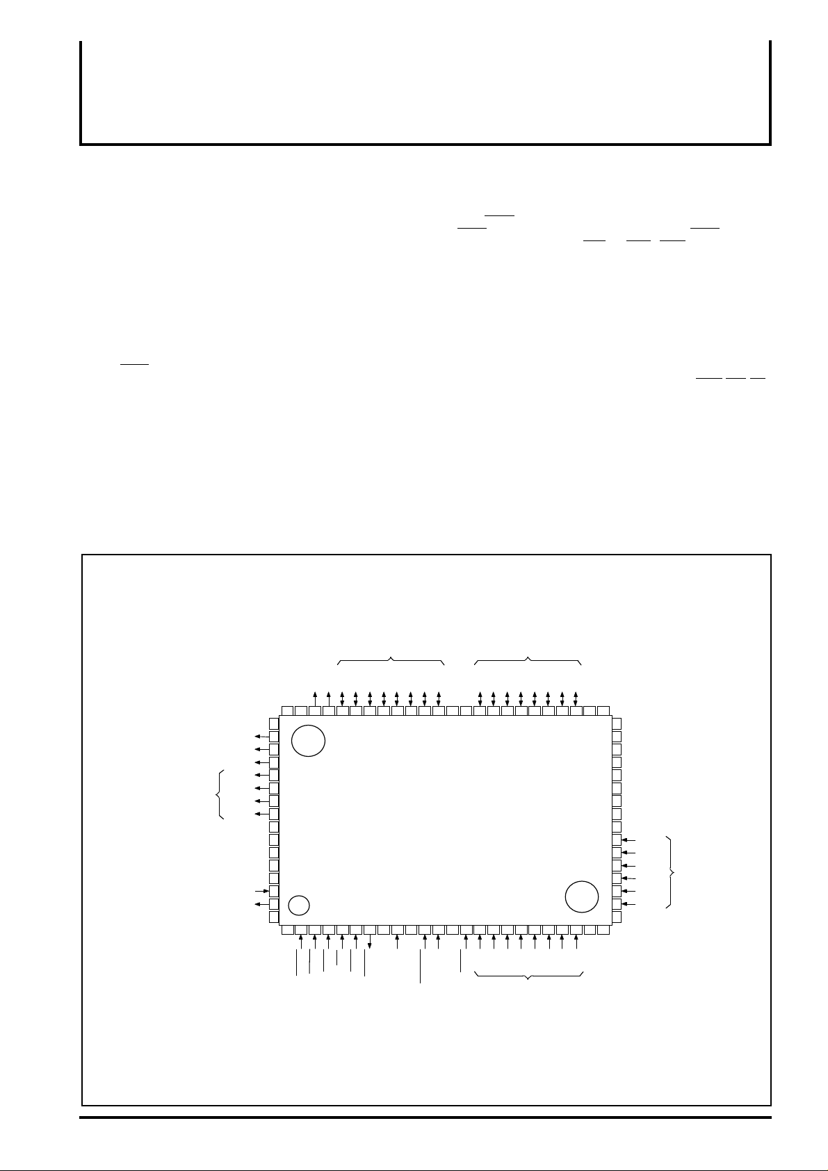
PIN CONFIGURATION(TOP VIEW)
VSS
6463626160595857565554535251504948474645444342
65
VSS
DISPLAY DATA TRANSFERCLOCK
DISPLAY DATA LATCH PULSE
FIRST LINE MARKER
LCD D ISPLAY DAT A BUS
OSCILLATORINPUT
OSCILLATOROUTPUT
UD<0>
UD<1>
UD<2>
UD<3>
OSC1
OSC2
CP
LP
FLM
N.C
N.C
N.C
N.C
V
VSS
66
67
68
69
70
71
72
73
74
75
76
77
DD
78
79
80
123456789
VSS
VDD
IOCS
LCD CONTROL SIGNAL
LCD ALTERNATING SIGNAL
LCDENB
M
LWRRDMCS
HWR
HIGH WR ITE STROBE
LOW WRITESTROBE
D<14>
D<15>
READ STROBE
VRAM CH IP SELECT
MPUDATABUS
D<9>
D<12>
D<13>
D<10>
D<11>
M66271FP
101112131415161718
VSS
VDD
WAIT
WAIT
RESET
MPUCLK
RESET
MPU CLOCK
SS
V
D<8>
VDD
VSS
BHE
MPUSEL
8/16MPU SELECT
BUS HIGH ENABLE
D<7>
A<0>
D<6>
A<1>
D<5>
D<4>
A<2>
MPUDATABUS
A<3>
MPU AD D R ESS BUS
D<3>
19
A<4>
A<5>
D<1>
A<6>
D<0>
A<7>
VDD
VDD
D<2>
2021222324
VSS
41
40
VSS
39
N.C
38
N.C
37
N.C
36
N.C
35
V
SS
34
VDD
33
N.C
32
N.C
31
A<13>
30
A<12>
29
A<11>
A<10>
A<9>
A<8>
VSS
MPU AD D R ESS BUS
28
27
26
25
VSS
Outline 80P6N-A
CONTROL REG ISTER CHIP SELECT
N.C : No Connection
MITSUBISHI <DIGITAL ASSP>
M66271FP
OPERATION PANEL CONTROLLER
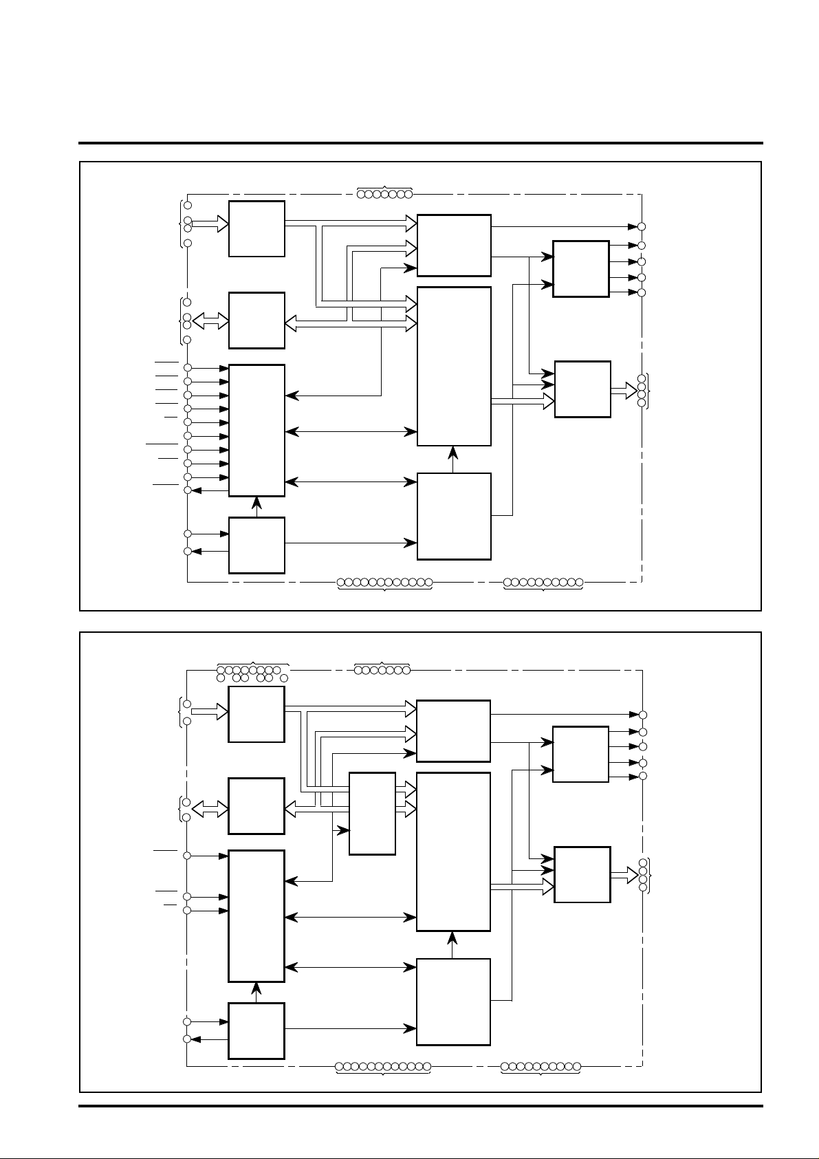
BLOCK DIAGRAM 1
15
–
IOCS
MCS
HWR
LWR
RD
RESET
BHE
WAIT
OSC1
OSC2
22
26
–
31
43
–
50
53
–
60
2
6
3
4
5
12
11
14
9
7
78
79
MPU ADDRESS
BUS
MPU DATA BUS
CONTROLREGISTER
CH I P SELECT
VRAMCH I P SELECT
HIGHWRITE STROBE
LOW WRITE S T ROBE
READ STROBE
8/16 MPU SELECT
RESET
BUS H IGH ENABLE
MPU CLOCK
WAIT
OSCILLATOR INPUT
OSCILLATOR OUTPUT
MPUSEL
MPUCLK
A<13:0>
D<15:0>
ADDRESS
BUFFER
DATA
BUFFER
MPU I/F
CONTROL
CIRCUIT
CLOCK
CONTROL
(BAS IC TIMING
CONTROL)
VDD
8 23 34 42 52 63 77
1 10 13 2425354041 516465
VSS
CONTROL
REGISTER
VRAM
9600byte
BUS ARBITER
TIMING
CONTROL
(CYCLE STEAL
CONTROL)
80
LCD DISPLAY
TIMING
CONTROL
CIRCUIT
LCD DISPLAY
DATA
CONTROL
CIRCUIT
32 33 36 37 38 39 73 74 75 76
N.C
61
LCDENB
66
CP
67
LP
68
FLM
62
M
69
70
UD<3:0>
71
72
LCD CONTROL
SIGNAL
DISPLAY DATA
TRANSFERCLOCK
DISPLA Y DATALATCH
PULSE
FIRSTLINE MARKER
SIGNAL
LCD ALTERNATING
SIGNAL
LCD DISPLAY
DATA BUS
BLOCK DIAGRAM 2 (In case of LCD module built-in system)
MPU ADDRESS
BUS
MPU DATA BUS
CONTROLREGISTER
CH I P SELECT
LOW WRITE S T ROBE
READ STROBE
OSCILLATOR INPUT
OSCILLATOR OUTPUT
A<4:1>
D<7:0>
IOCS
LWR
OSC1
OSC2
RD
NO USE PINS
6
3
9 111214
15
7
20
31
22 26
53
–
–60–
16
–
19
43
–
50
2
4
5
78
79
ADDRESS
BUFFER
DATA
BUFFER
MPU I/F
CONTROL
CIRCUIT
CLOCK
CONTROL
(BAS IC TIMING
CONTROL)
10 13 24 25
1
VDD
8
233442 52 63
VRAM
ADDRESS
INDEX
REGISTER
DATAPORT
REGISTER
35
VSS
404151
77
BUS ARBITER
TIMING
CONTROL
80
64
65
CONTROL
REGISTER
VRAM
9600byte
LCD DISPLAY
TIMING
CONTROL
CIRCUIT
LCD DISPLAY
DATA
CONTROL
CIRCUIT
32 33 36 37 38 39 73 74 75 76
N.C
61
LCDENB
CP
66
67
LP
FLM
68
62
M
69
70
UD<3:0>
71
72
LCD CONTROL
SIGNAL
DISPLAY DATA
TRANSFERCLOCK
DISPLA Y DATALATCH
PULSE
FIRSTLINE MARKER
SIGNAL
LCD ALTERNATING
SIGNAL
LCD
DISPLAY
DATA BUS

PIN DESCRIPTIONS
Item
MPU
interface
LCD
interface
Oscillator
Others
Pin
name
D<15:0> 16
A<13:0> 14
IOCS
MCS
HWR
LWR
RD
MPUSEL
RESET
MPUCLK 1
BHE
WAIT
UD<3:0>
LP
SS
N.C
Input/
Output
Input/
Output
Input
Input
Input
Input
Input
Input
Input
Input
Input
Input
Output
Output
Output
Output
Output
Output
Output
Input Input pin for oscillator
Output Output pin for oscillator
MITSUBISHI <DIGITAL ASSP>
M66271FP
OPERATION PANEL CONTROLLER
Function
MPU data bus
Connect to MPU data bus.
Selecting 8bit MPU by MPUSEL input, D<15:8> connect to VDD or VSS.
MPU address bus
Connect to MPU address bus. When selecting 8-bit MPU, use A<13:0>. And selecting
16-bit MPU, use A<13:1> for the address bus with combining A<0> and BHE by the method
of access to internal VRAM (Refer to Figure-1). Use A<4:0> for selecting address of control register.
Chip select input of control register
When this pin is "L", select the internal control register. Assign to I/O space of MPU.
Chip select input of VRAM
When this pin is "L", select the internal VRAM. Assign to memory space of MPU.
High-Write strobe input
When this pin is "L", data write to the internal VRAM. HWR is valid only in using 16-bit MPU
controlled byte access by LWR and HWR. (Refer to Figure-1)
Low-Write strobe input
When this pin is "L", data write to the internal control register or VRAM. (Refer to Figure-1)
Read strobe input
When this pin is "L", data read from the internal control register or VRAM.(Refer to Figure-1)
8/16-bit MPU select input
According to MPU, set "V
Reset input
Use reset signal of MPU.When this pin is "L", initialize all internal control register and counter.
MPU clock
Input of MPU clock.
Bus-High-Enable input
This pin is valid when using 16-bit MPU controlled byte access by A<0> and BHE (Refer to Figure-
1). Connect to "V
Set to "L" when using the additional function for the LCD Module built-in system.
WAIT output for MPU
This signal makes WAIT for MPU.
Change WAIT "L" at timing of falling edge of overlapping with MCS and (RD or LWR or HWR).
And return to "H" at synchronizing with the rising edge of MPUCLK after internal processing.
(Output WAIT only when requested access from MPU to VRAM during cycle steal access.)
Display data bus for LCD
Transfer the LCD display data with 4-bit parallel signal.
Mutually output upper/lower data every CP output.
Display data transfer clock
Shift clock for the transfer of display data to LCD.
Take the display data of UD<3:0> to LCD at falling edge of CP.
Display data latch pulse
This clock use both as the latch pulse of display data for LCD and the transfer of scanning signal.
LP output when finish the transfer of display data of a line.
Latch of display data and the transfer of scanning signal at falling edge of LP.
First line marker signal
Output the start pulse of scanning line.
This signal is "H" active,the IC for driving scanning line catch FLM at falling edge of LP.
LCD alternating signal output
Signal for driving LCD by alternating current.
LCD(ON/OFF) control signal output
Output data which is set at bit"0 " of mode register(R1) in control register. This signal can use
for controlling the LCD power supply, because LCDENB set to "L" byRESET.
Power supply.(source +5V )
Ground
No connection
SS" for 8bit MPU and set "VDD" for 16bit MPU.
DD" when using 8-bit MPU.
Generate an internal clock.
For crystal oscillator or external clock signal.
Number
of pins
1
1
1
1
1
1
1
1
1
4
1CP
1
1FLM
1M
1LCDENB
1OSC1
1OSC2
7VDD
12V
10
MITSUBISHI <DIGITAL ASSP>
M66271FP
OPERATION PANEL CONTROLLER
OUTLINE
M66271FP is graphic display only controller for displaying a dot
matrix type LCD. This IC has a built-in display data memory
(VRAM) which is equivalent to 320
×240 dots LCD.
●Control register
When access the control register from MPU side, use IOCS,
LWR,RD,A<4:0> and D<7:0>. Refer to Table-1,when set control
type inputs.
Control registers are R1 – R8 for the normal mode function and
R9 – R11 for the exclusive register for the LCD module built-in
system.
●VRAM
When access VRAM from MPU side, use MCS,HWR,LWR,
RD,BHE, A<13:0> and D<15:0>. And enable to correspond to
both 8-bit and 16-bit MPU by using MPUSEL input. Refer to
Figure-1 and Table-2 – 6 for a form of VRAM and input setting
for 8/16-bit MPU.
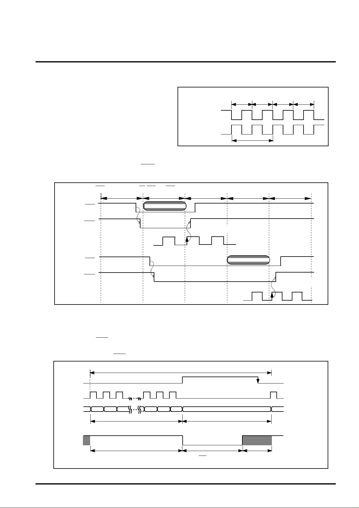
●Cycle steal system
Cycle steal is interact method of transferring display data for
LCD from VRAM and accessing VRAM from MPU on the basic
cycle of OSC.
Basic timing is two clocks of OSC,and assign first clock to the
access from MPU to VRAM and second clock to the transfer of
display data from VRAM to LCD.
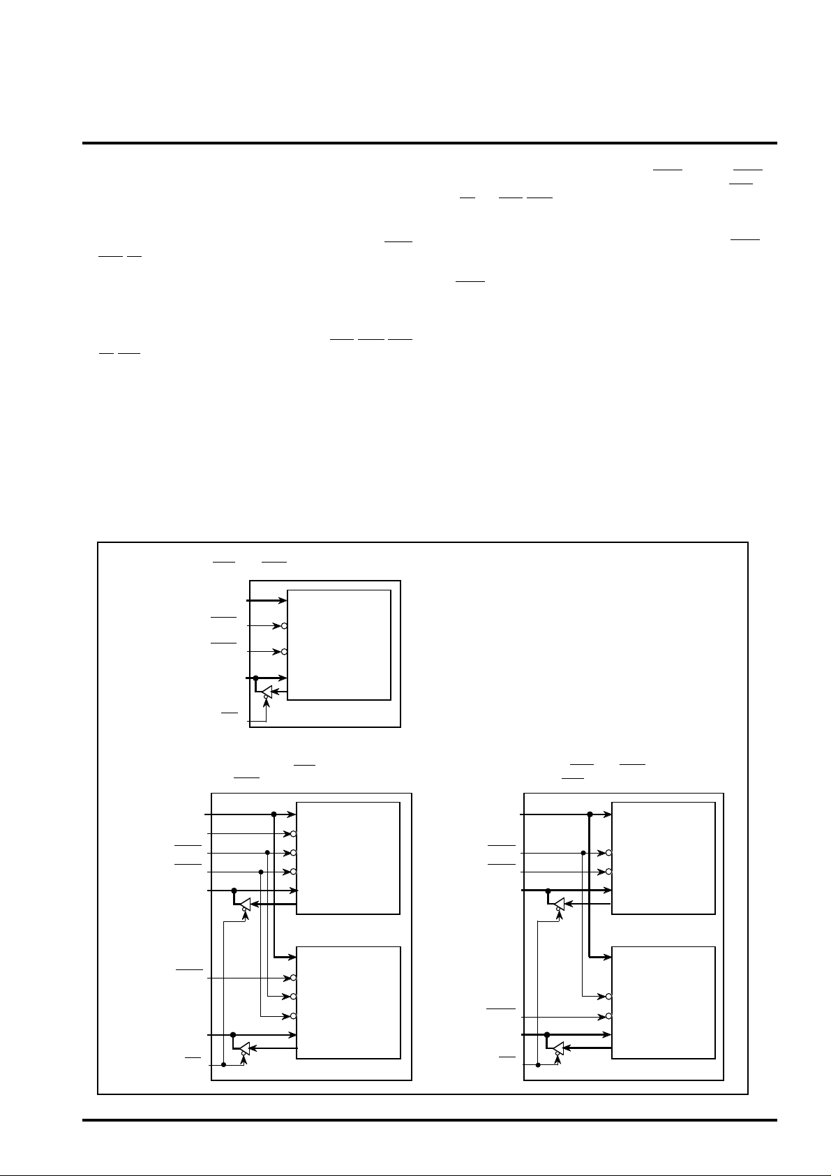
Difference in VRAM between 8-bit and 16-bit MPU
(1) When accessing built-in VRAM by 8-bit MPU
(MPUSEL="L",BHE="H",HWR="H" :set)
In accessing VRAM from MPU,output WAIT. Change WAIT to
"L" at the timing of the falling edge of overlapping with MCS and
(RD or LWR/HWR). And return to "H" at synchronizing with
rising edge of MPUCLK after internal processing.
Cycle steal system can transfer data with more efficient. This
function access with the cycle steal method as taking WAIT for
MPU during the display term with necessity for the display data
transfer from built-in VRAM to LCD. On other side, don't output
WAIT for keeping throughput of MPU during horizontal
synchronous term with no necessity for the display data transfer
from VRAM to LCD side.
Refer to the following description of cycle steal.
●Output to LCD side
LCD display data UD<3:0> output synchronized with the rising
edge of CP output per 4bits.
LP output synchronized with the falling edge of OSC when finish
the transfer of display data for a line.
Enable to adjust the fittest value of the frame frequency
requested by the LCD PANEL side with adjusting pulse width by
LPW register.
FLM output, when finish the transfer of display data of 1st line.
M output is the LCD alternating signal which is signal for driving
LCD by alternating current.
M-cycle enable to set variably by M-cycle variable register in
line unit, and enable to utilize for preventting LCD from being
inferior.
A<13:0>
MCS
LWR
D<7:0>
A<13:0>
CEC
WEC
DI<7:0>
DO<7:0>
VRAM
9600byte
RD
(2) When accessing built-in VRAM by 16-bit MPU
(2-1) In case MPU use A<0> and BHE for byte access
(MPUSEL="H",HWR="H":set)
A<13:1>
A<0>
MCS
LWR
A<13:1>
A<0>
CEC
WEC
VRAM
4800byte
(Lower byte)
D<7:0> DI<7:0>
DO<7:0>
A<13:1>
BHE
D<15:8> DI<15:8>
A<0>
CEC
WEC
DO<15:8>
VRAM
4800byte
(Upper byte)
RD
(2-2) In case MPU use LWR and HWR for byte access
(MPUSEL="H",BHE="H",A<0>="H":set)
A<13:1>
MCS
LWR
D<7:0>
HWR
D<15:8> DI<15:8>
A<13:1>
CEC
WEC
DI<7:0>
DO<7:0>
A<13:1>
CEC
WEC
DO<15:8>
VRAM
4800byte
(Lower byte)
VRAM
4800byte
(Upper byte)
RD
Figure-1 Difference in VRAM between 8-bit and 16-bit MPU
OPERATION PANEL CONTROLLER
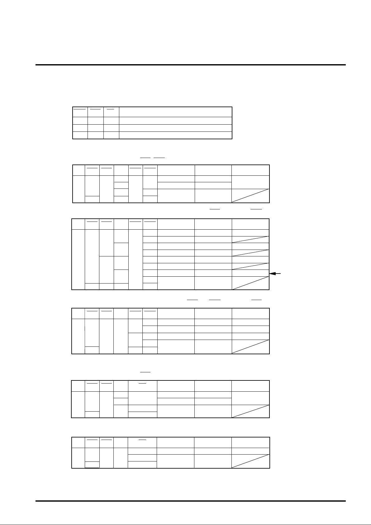
Combination of control input pins for MPU interface
Table-1 – 6 show conditions of input setting when access the control register and VRAM from MPU
(1) Access control register (Use address=A<4:0>,Data=D<7:0>)
Table-1
LHL
LLH
HXX
Write to control register
Read from control register
Invalid
(2) Writing to VRAM
(2-1) When use 8-bit MPU (MPUSEL="L",BHE=HWR="H":set)
Table-2
MPU
SEL
LHL
L
A<0>BHEMCS HWR LWR
HL
H
XH
HXX
OperationIOCS LWR RD
Odd address Even address
Invalid Write
Write
Invalid
Invalid Invalid
Valid data bus
width of MPU
8-bit
MITSUBISHI <DIGITAL ASSP>
M66271FP
(2-2) When use 16-bit MPU (In MPU controls byte access with A<0> and BHE. MPUSEL=HWR="H":set)
Table-3
MPU
SEL
A<0>BHEMCS HWR LWR
LLLH
H
L
H
H
XXH
HL
H
L
H
L
H
L
H
X
Upper byte Lower byte
Write
Invalid
Write
Invalid
Write Invalid
Invalid Invalid
Invalid Write
Invalid Invalid
Invalid Write
Invalid Invalid
Valid data bus
width of MPU
16-bit
Upper 8-bit
Lower 8-bit
Lower 8-bit
Even if A<0>="H",
enable to write
(2-3) When use 16-bit MPU (In MPU controls byte access with LWRand HWR. MPUSEL=BHE=A<0>="H":set)
Table-4
MPU
SEL
A<0>BHEMCS HWR LWR
LLHHLH
H
H
XX
Upper byte Lower byte
Write Write
H
L
H
Write
Invalid Write
Invalid Invalid
Invalid
Valid data bus
width of MPU
16-bit
Upper 8-bit
Lower 8-bit
(3) Reading from VRAM
(3-1) When use 8-bit MPU (MPUSEL="L",BHE="H":set)
Table-5
MPU
SEL
L
MCS
L
H
BHE
H
A<0> RD
L
L
H
X
H
X
Odd address Even address
Invalid
Read
Read
Invalid
Invalid Invalid
Valid data bus
width of MPU
8-bit
(3-2) When use 16-bit MPU (MPUSEL="H":set)
MPU
MCS
BHE
Table-6
SEL
H
LXX
A<0> RD
L
H
H
X
Note:Avoid setting combination except above,as cause of error action
:X="L" or "H"
Upper byte Lower byte
Read Read
Invalid Invalid
Valid data bus
width of MPU
16-bit
Description of cycle steal
MITSUBISHI <DIGITAL ASSP>
M66271FP
OPERATION PANEL CONTROLLER
BASIC TIMING
Basic timing of M66271FP is two clocks of OSC
(internal clock after dividing OSC1 input).
Assign first clock to accessing from MPU to VRAM
and second clock to transferring of display data
from VRAM to LCD
Operation cycle of MPU access(during WAIT output)
Writing or Reading operation for VRAM during cycle steal
needs 1 cycle in best case or 3 cycles in worst case,
Ex.) Assuming that MCS input is later than RD,LWR and HWR input.
Best case
MCS
WAIT
Cycle of
LCD access
Cycle of
MPU access
Operation cycle of MPU access
MPUCLK
Worst case
MCS
OSC
(Internal clock after
dividing OSC1 input)
CP output
(Display data transfer)
Figure-2 BASIC TIMING
according to the condition of the internal cycle steal at staring
access requested from MPU.
Cycle of
LCD access
Cancel WAIT,when synchronize
with rising edge of MPUCLK
Access
from MPU
to VRAM
Data transfer
from VRAM
to LCD
Basic cycle
Cycle of
MPU access
Ope ration cycle of MPU a ccess
Cycle of
LCD access
LCDMPU
WAIT
Figure-3 Operation cycle of MPU access
Function of cycle steal control
M66271FP has a function for processing data of a line with
more efficient. This function access with the cycle steal
method as taking WAIT for MPU during the display term
with necessity for the display data transfer from built-in
VRAM to LCD.
On other side, don't output WAIT for keeping throughput of
Ex.) Assuming 320×240 dots LCD
LP
UD<3:0>
CSE
(Internal signal)
CP
1 23
Setting by CR register
Displaying term (Cycle steal method)
(Necessity for data transfer from VRAM to LCD side)
Start WAIT for MPU according to
cycle steal access.
78 79 80
MPUCLK
MPU during the horizontal synchronous term with no necessity
for the display data transfer from VRAM to LCD side.
But certainly set a term of accessing with the cycle steal
method by CSW register, for controlling an error action near
the end of horizontal synchronous term.
1 Line
Setting by LPW register
Horizontal synchronous term
(No necessity for data transfer from VRAM to LCD side)
Access with bus timing of MPU
without WAIT for MPU.
Cancel WAIT,when synchronize
with rising edge of MPUCLK
Output when finish transfer
of display data with a line
1
Output every transfer of
a display data
4bit transfer
Setting by CSW register
Start WAIT for MPU in timing of CSE "H"
according to bus timing of MPU.
Figure-4 Function of cycle steal control
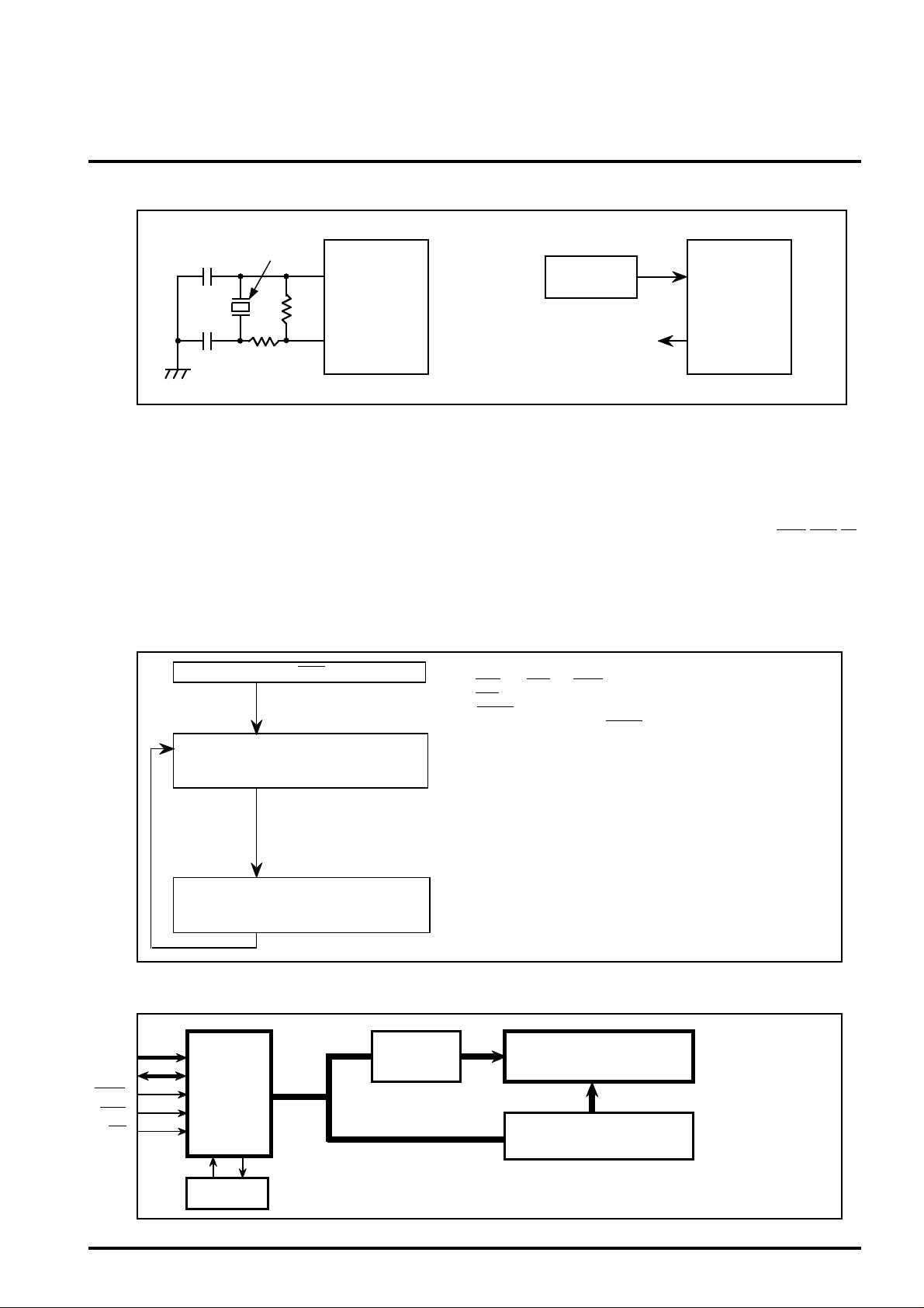
Handling of oscillator pin
<1> Crystal oscillator <2> Input from external clock directly
Crystal oscillator
C1
Rf
OSC1
M66271FP
MITSUBISHI <DIGITAL ASSP>
M66271FP
OPERATION PANEL CONTROLLER
Clock
generator
OSC1
M66271FP
OSC2
C2
As far as possible, connect C,R and the crystal oscillator at near the pin.
Figure-5 Oscillator pin
Rd
Additional function for LCD module built-in system
As all of the VRAM address in M66271FP are
externally opened for addressing VRAM from MPU
directly.
When consider the LCD module built-in system,connect
pins are increased.
But M66271FP has an additional function for the LCD
module built-in system by lessening connect pins.
Setting to MPUSEL,BHE="L"
Select VRAM address index register (IDXL,
IDXH),and write access address(14bit) as
data.
Open
Outline of the additional function for the LCD module built-in system
●Interface pins with MPU
15 kinds of Interface with MPU:A<4:1>,D<7:0>,IOCS,LWR,RD
●Method of accessing the internal VRAM
Access the internal VRAM through the VRAM address index
register (IDXL,IDXH) and the Data port register (DP) which are
used for I/O register.
The following show the process of accessing VRAM.
●No use pins set the following.
HWR="H",MCS="H",WAIT= open,MPUCLK="L",MPUSEL="L",
BHE="L",A<0>="L",A<13:5>="L",D<15:8>="L",
● RESET=Power on reset or soft ware reset.
(In case of soft ware reset RESET ="H" :set)
●Enable to change IDXL and IDXH,even if either.
●Access the DP after writing the mode register (DISP(R1-D2)) =" 0".
Always enable to access (CSES register ="0"),because the display
signal fix "H" or "L" in DISP="0" and a term is no wait access.
●Access DP without WAIT function.
OSC2
Select Data port register (DP).
Reading/Writing data for appointed
VRAM address.
VRAM address is increased of +1.
Application
MPU side LCD side
A<4:1>
D<7:0>
IOCS
LWR
RD
M66271FP
Crystal
Oscillator
Common
driver
●VRAM address is automatically increased of +1 ,when finished
access to DP.
When access to continuous address,it doesn't need to set IDXL
and IDXH.
Graphic LCD PANEL
Segment driver
LCD module of small size for only graphics
 Loading...