

MITSUBISHI 〈DIGITAL ASSP〉
MITSUBISHI 〈DIGIT AL ASSP〉
DESCRIPTION
The M66257FP is a high-speed line memory with a FIFO
(First In First Out) structure of 5120-word × 8-bit double configuration which uses high-performance silicon gate CMOS
process technology.
It allows simultaneous output of 1-line delay data and 2-line
delay data, and is most suitable for data correction over multiple lines.
It has separate clock, enable and reset signals for write and
read, and is most suitable as a buffer memory between devices with different data processing throughput.
FEATURES
• Memory configuration of 5120 words × 8 bits × 2 (dynamic
memory)
• High-speed cycle ............................................. 25ns (Min.)
• High-speed access ......................................... 18ns (Max.)
• Output hold ........................................................ 3ns (Min.)
• Fully independent, asynchronous write and read operations
• Output ....................................................................3 states
00 to Q07........................................................ 1-line delay
•Q
10 to Q17........................................................ 2-line delay
•Q
APPLICATION
Digital photocopiers, high-speed facsimile, laser beam printers.
M66257FP
5120 × 8-BIT × 2 LINE MEMORY (FIFO)
5120 × 8-BIT × 2 LINE MEMORY (FIFO)
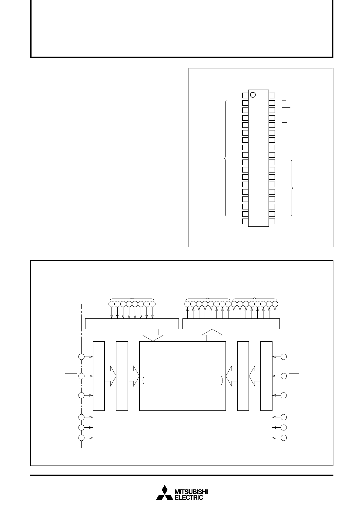
PIN CONFIGURATION (TOP VIEW)
DATA OUTPUT
GND
Q00
Q
Q
Q
Q
Q
Q
Q
Q
Q
Q
Q
Q
Q
Q
Q
V
CC
1
←
←
01
3
←
02
4
←
03
5
←
04
6
←
05
7
←
06
8
←
07
9
←
10
10
←
11
11
←
12
12
←
13
13
←
14
14
←
15
15
←
16
16
←
17
17
18
Outline 36P2R-A
36
352
34
33
32
31
30
M66257FP
29
28
27
26
25
24
23
22
21
20
19
M66257FP
CC
V
←
←
←
←
←
←
←
←
←
←
←
←
←
←
READ ENABLE INPUT
RE
READ RESET INPUT
RRES
READ CLOCK INPUT
RCK
WRITE ENABLE INPUT
WE
WRITE RESET INPUT
WRES
WRITE CLOCK INPUT
WCK
GND
V
CC
0
D
1
D
2
D
3
D
DATA INPUT
4
D
5
D
6
D
7
D
GND
BLOCK DIAGRAM
WRITE
ENABLE INPUT
WRITE
RESET INPUT
WRITE
CLOCK INPUT
WE
WRES
WCK
CC
DATA INPUT
0 D7
D
2726252423222120 234567891011121314151617
INPUT BUFFER
32
31
30
WRITE CONTROL CIRCUIT
18V
28VCC
36VCC
5120-WORD × 8-BIT × 2 CONFIGURATION
WRITE ADDRESS COUNTER
MEMORY ARRAY OF
1-LINE DELAY DATA ONLY MEMORY/
2-LINE DELAY DATA ONLY MEMORY
DATA OUTPUT
~~~
Q
00 Q07
OUTPUT BUFFER
DATA OUTPUT
Q
10 Q17
35
34
33
READ ADDRESS COUNTER
READ CONTROL CIRCUIT
1 GND
19 GND
29 GND
RE
RRES
RCK
READ
ENABLE INPUT
READ
RESET INPUT
READ
CLOCK INPUT
1

MITSUBISHI 〈DIGITAL ASSP〉
M66257FP
5120 × 8-BIT × 2 LINE MEMORY (FIFO)
FUNCTION
When write enable input WE is “L”, the contents of data inputs
0 to D7 are written into 1-line delay data only memory in syn-
D
chronization with rise edge of write clock input WCK. At this
time, the write address counter of 1-line delay data only
memory is also incremented simultaneously.
The write functions given below are also performed in synchronization with rise edge of WCK.
When WE is “H”, a write operation to 1-line delay data only
memory is inhibited and the write address counter of 1-line
delay data only memory is stopped.
When write reset input WRES is “L”, the write address counter
of 1-line delay data only memory is initialized.
When read enable input RE is “L”, the contents of 1-line delay
data only memory are output to data outputs Q
those of 2-line delay data only memory to data outputs Q
17 in synchronization with the rise of read clock input RCK.
Q
00 to Q07 and
10 to
At this time, the read address counters of 1-line and 2-line
delay data only memories is also incremented simultaneously.
Moreover, data of Q00 to Q07 are written into 2-line delay data
only memory in synchronization with rise edge of RCK. At
this time, the write address of 2-line delay data only memory
is incremented.
The read functions given below are also performed in synchronization with rise edge of RCK.
When RE is “H”, a read operation from both of 1-line delay
data only memory and 2-line delay data only memory is inhibited and the read address counter of each memory is
stopped. The outputs of Q
00 to Q07 and Q10 to Q17 are in the
high impedance state.
Moreover, a write operation to 2-line delay data only memory
is inhibited and the write address counter of 2-line delay data
only memory is stopped.
When read reset input RRES is “L”, the read address counter
of 1-line delay data only memory, and the write address
counter and read address counter of 2-line delay data only
memory are initialized.
2
ABSOLUTE MAXIMUM RATINGS (Ta = 0 ~ 70°C, unless otherwise noted)
VCC
VI
VO
Pd
Tstg
Symbol
Supply voltage
Input voltage
Output voltage
Maximum power dissipation
Storage temperature
Parameter
A value based on GND pin
Ta = 25°C
RECOMMENDED OPERATING CONDITIONS
Parameter
Min.
4.5
0
VCC
GND
Topr
Symbol
Supply voltage
Supply voltage
Operating ambient temperature
Conditions
Limits
Typ.
5
0
MITSUBISHI 〈DIGITAL ASSP〉
M66257FP
5120 × 8-BIT × 2 LINE MEMORY (FIFO)
Unit
V
V
V
mW
°C
Max.
5.5
70
Ratings
–0.5 ~ +7.0
–0.5 ~ VCC + 0.5
–0.5 ~ VCC + 0.5
660
–65 ~ 150
Unit
V
V
°C
ELECTRICAL CHARACTERISTICS (Ta = 0 ~ 70°C, VCC = 5V ± 10%, GND = 0V, unless otherwise noted)
Parameter
Test conditions
IOH = –4mA
IOL = 4mA
VI = VCC
VI = GND
VO = VCC
VO = GND
VI = VCC, GND, Output open
tWCK, tRCK = 25ns
f = 1MHz
f = 1MHz
WE, WRES, WCK, RE,
RRES, RCK,
D0 ~ D7
WE, WRES, WCK, RE,
RRES, RCK,
D0 ~ D7
2.0
VCC–0.8
VIH
VIL
VOH
VOL
IIH
IIL
IOZH
IOZL
ICC
CI
CO
Symbol
“H” input voltage
“L” input voltage
“H” output voltage
“L” output voltage
“H” input current
“L” input current
Off state “H” output current
Off state “L” output current
Operating mean current dissipa-
tion
Input capacitance
Off state output capacitance
Limits
Typ.Min.
Max.
0.8
0.55
1.0
–1.0
5.0
–5.0
120
10
15
Unit
V
V
V
V
mA
mA
mA
mA
mA
pF
pF
3

5120 × 8-BIT × 2 LINE MEMORY (FIFO)
SWITCHING CHARACTERISTICS (Ta = 0 ~ 70°C, VCC = 5V ± 10%, GND = 0V, unless otherwise noted)
Parameter
tAC
tOH
tOEN
tODIS
Symbol
Access time
Output hold time
Output enable time
Output disable time
TIMING CONDITIONS (Ta = 0 ~ 70°C, VCC = 5V ± 10%, GND = 0V, unless otherwise noted)
Symbol
tWCK
tWCKH
tWCKL
tRCK
tRCKH
tRCKL
tDS
tDH
tRESS
tRESH
tNRESS
tNRESH
tWES
tWEH
tNWES
tNWEH
tRES
tREH
tNRES
tNREH
tr, tf
tH
Note 1: For 1-line access, the following should be satisfied:
WE “H” level period < 20ms – 5120 t
RE “H” level period < 20ms – 5120 t
2: Reset the IC after power is turned on.
Write clock (WCK) cycle
Write clock (WCK) “H” pulse width
Write clock (WCK) “L” pulse width
Read clock (RCK) cycle
Read clock (RCK) “H” pulse width
Read clock (RCK) “L” pulse width
Input data setup time to WCK
Input data hold time to WCK
Reset setup time to WCK or RCK
Reset hold time to WCK or RCK
Reset nonselect setup time to WCK or RCK
Reset nonselect hold time to WCK or RCK
WE setup time to WCK
WE hold time to WCK
WE nonselect setup time to WCK
WE nonselect hold time to WCK
RE setup time to RCK
RE hold time to RCK
RE nonselect setup time to RCK
RE nonselect hold time to RCK
Input pulse rise/fall time
Data hold time (Note 1)
WCK – WRES “L” level period
RCK – RRES “L” level period
Parameter
MITSUBISHI 〈DIGITAL ASSP〉
M66257FP
25
11
11
25
11
11
Limits
Typ.Min.
3
3
3
Limits
Typ.Min.
7
3
7
3
7
3
7
3
7
3
7
3
7
3
Max.
18
18
18
Max.
20
20
Unit
ns
ns
ns
ns
Unit
ns
ns
ns
ns
ns
ns
ns
ns
ns
ns
ns
ns
ns
ns
ns
ns
ns
ns
ns
ns
ns
ms
4

TEST CIRCUIT
MITSUBISHI 〈DIGITAL ASSP〉
M66257FP
5120 × 8-BIT × 2 LINE MEMORY (FIFO)
V
CC
RL=1kΩ
Q
n
SW1
Q
CL=30pF : tAC, t
OH
n
SW2
R
L
=1kΩ
CL=5pF : t
OEN
, t
ODIS
Input pulse level : 0 ~ 3V
Input pulse rise/fall time : 3ns
Decision voltage input : 1.3V
Decision voltage output : 1.3V (However, t
The load capacitance C
probe.
that for decision).
L includes the floating capacitance of connection and the input capacitance of
tODIS/tOEN TEST CONDITION
RCK
RE
1.3V
tODIS(HZ)
ODIS(LZ) is 10% of output amplitude and tODIS(HZ) is 90% of
Parameter
tODIS(LZ)
tODIS(HZ)
tOEN(ZL)
tOEN(ZH)
1.3V
OEN(ZH)
t
SW1
Closed
Open
Closed
Open
SW2
Open
Closed
Open
Closed
3V
GND
3V
GND
Q
Q
Q0n
Q
OH
V
VOL
tODIS(LZ)
90%
10%
1.3V
tOEN(ZL)
1.3V
0n
1n
1n
5

OPERATING TIMING
• Write cycle
WCK
MITSUBISHI 〈DIGITAL ASSP〉
M66257FP
5120 × 8-BIT × 2 LINE MEMORY (FIFO)
Cycle n Cycle n+1 Cycle n+2 Disable cycle Cycle n+3 Cycle n+4
WE
n
D
• Write reset cycle
t
WCK
t
WCKHtWCKLtWEHtNWES
tDSt
DH
(n)
t
t
NWEH
WES
t
t
DS
DH
(n+2) (n+3)( n+1)(n) (n+4)
WRES = “H”
WCK
WRES
n
D
Cycle n–1 Cycle n Reset cycle Cycle 2Cycle 0 Cycle 1
t
WCK
t
NRESHtRESS
tDHt
tDHt
DS
(n–1) (n) (0) (1) (2)
DS
t
RESHtNRESS
WE = “L”
6

• Read cycle
RCK
RE
0n
Q
Q
1n
Cycle n Disable cycle Cycle n+3 Cycle n+4Cycle n+2Cycle n+1
t
RCK
t
RCKHtRCKLtREHtNRES
(n) (n+1) (n+2) (n+3) (n+4)
t
ODIS
t
NREHtRES
HIGH-Z
MITSUBISHI 〈DIGITAL ASSP〉
M66257FP
5120 × 8-BIT × 2 LINE MEMORY (FIFO)
AC
t
t
OEN
t
OH
• Read reset cycle
RCK
RRES
Cycle n–1 Cycle 0 Cycle 2Cycle n Reset cycle Cycle 1
t
RCK
t
NRESHtRESS
t
RESHtNRESS
t
AC
RRES = “H”
Q
0n
(n–1) (n) (0) (0) (0) (1) (2)
Q
1n
t
ON
t
ON
t
ON
RE = “L”
7

• Note at WCK stop
WCK
WE
MITSUBISHI 〈DIGITAL ASSP〉
5120 × 8-BIT × 2 LINE MEMORY (FIFO)
n cycle n+1 cycle n cycle Disable cycle
t
tWCK
tDS tDH tDS tDH
NWES
M66257FP
n
D
(n)
Period of writing data (n)
into memory
(n)
Period of writing data (n)
into memory
WRES = “H”
Input data Dn of n cycle is read at the rising edge after WCK of n cycle. Writing operation starts in the “L” period of WCK of n+1
cycle and ends at the rising edge after n+1 cycle.
To stop reading write data at n cycle, input WCK for up to the rising edge of n+1 cycle.
When the cycle next to n cycle is a disable cycle, input of WCK for a cycle is required after a disable cycle as well.
8

MITSUBISHI 〈DIGITAL ASSP〉
M66257FP
5120 × 8-BIT × 2 LINE MEMORY (FIFO)
• Shortest read of data “n” written in cycle n
Cycle n–1 on read side should be started after end of cycle n+1 on write side
When the start of cycle n–1 on read side is earlier than the end of cycle n+1 on write side, output Qn of cycle n becomes invalid.
In the figure shown below, the read of cycle n–1 is invalid.
Cycle n Cycle n+1 Cycle n+2 Cycle n+3
WCK
D
n
RCK
Q
n
Cycle n–2 Cycle n–1 Cycle n
invalid (n)
(n+3)(n) (n+2)(n+1)
• Longest read of data “n” written in cycle n: 1-line delay
Cycle n <1>* on read side should be started when cycle n <2>* on write is started
Output Qn of n cycle <1>* can be read until the start of reading side n cycle <1> and the start of writing side n cycle <2>* overlap each other.
Cycle n <1>* Cycle 0 <2>* Cycle n <2>*
WCK
D
n
RCK
Q
(n–1)<2>* (n)<2>*(n–1)<1>* (0) <2>*(n)<1>*
Cycle n <0>* Cycle 0 <1>* Cycle n <1>*
n
(n–1)<0>*
(n)<0>*
(0)<1>* (n–1)<1>* (n)<1>*
<0>*, <1>* and <2>* indicates a line value.
9

5120 × 8-BIT × 2 LINE MEMORY (FIFO)
APPLICATION EXAMPLE
Laplacian Filter Circuit for Correction of Resolution in the Secondary Scanning Direction.
N
Line n image data
×2
B
Line (n+1)
image data
M66257
D
0
D
7
1-line
delay
Q
00
Q
07
MITSUBISHI 〈DIGITAL ASSP〉
M66257FP
Corrected
image data
Adder
{2N–(A+B)}
N+K
Primary scanning
direction
Secondary scanning
direction
×K
2N–(A+B)
Subtractor
A
Line (n–1)
Q
10
Q
17
2-line
delay
A
N
B
image data
A+B
Adder
Line (n–1)
Line n
Line (n+1)
N' = N+K {
(N–A)+(N–B)}
= N+K {
2N–(A+B)}
K : Laplacean coefficient
10
 Loading...