

The M66244FP is a high-speed digitally programmable pulse width modulator (PWM) which
uses high-performance silicon gate CMOS process technology.Output pulse width is
proportional to a 6-bit DATA input value. Two additional CONTROL inputs determine if the
pulse is placed at the beginning , middle ,or end of the clock period. Pulse width and
placement can be changed every clock cycle up to 72MHz.
FEATURES
• Frequency 45MHz to 72MHz
• 6 bit Resolution
• Center, Leading, Trailing Edge Modulation
• Single 3.3V Operation
• JTAG (IEEE Standard 1149.1Test Port)
PRELIMINARY DATA SHEET
DATA BUS
INPUT
PRELIMINARY DATA SHEET
MITSUBISHI <DIGITAL ASSP>
M66244FP
June 1998 Ver.8.0.0
High Speed Monolithic Pulse Width Modulator
NOTE:This is not final specification. Some parametric limits are subject to change
DESCRIPTION
APPLICATIONS
• Laser Printers
Gray Scale Capability
Resolution Enhancement
• Copiers
• Optical Disk Drives
• Precision Pulse Placement
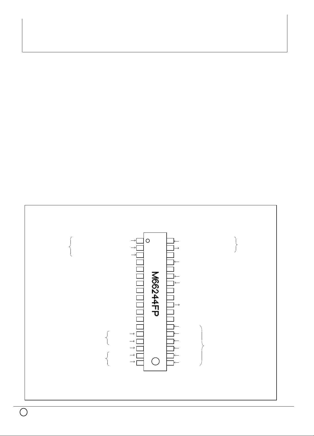
PIN CONFIGURATION (TOP VIEW)
TEST PIN
(JTAG)
TEST CLOCK INPUT
TEST MODE INPUT
FREQUENCY
RANGE SET INPUT
LINE SIGNAL INPUT
PULSE MODE
CONTROL
INPUT
TCK
TMS
TRSTTEST RESET INPUT
GND
VDD
GND
VDD
GND
VDD
GND
VDD
GND
VDD
FRANGE1
FRANGE2
LS
SEM/DEM
LEM/TEM
1
2
3
4
5
6
7
8
9
10
11
12
13
14
15
16
17
18
36
TDI
35
TDO
34
GND
33
CLK CLOCK INPUT
32
VDD
31
RESET
30
SET
29
VDD
28
GND
27
PWMOUT
VDD
26
GND
25
24
23
22
21
20
19
D0(LSB)
D1
D2
D3
D4
D5(MSB)
TEST DATA INPUT
TEST DATA OUTPUT
RESET INPUT
SET INPUT
TEST PIN
(JTAG)
C 1998 MITSUBISHI ELECTRIC CORPORATION
Outline 36P2R
(1/15)
FRANGE1 and FRANGE2 are set up correspond to
operation frequency range (refer to page 8)
June 1998 Ver.8.0.0
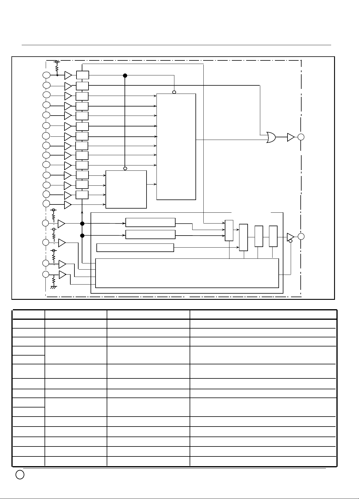
BLOCK DIAGRAM
MITSUBISHI <DIGITAL ASSP>
M66244FP
High Speed Monolithic Pulse Width Modulator
RESET
SET
D0(LSB)
D1
D2
D3
D4
D5(MSB)
LEM/TEM
SEM/DEM
LS
FRANGE2
FRANGE1
CLK
TDI
TRST
31
30
24
23
22
21
20
19
18
17
16
15
14
33
BSR
BSR
BSR
BSR
BSR
BSR
BSR
BSR
BSR
BSR
BSR
BSR
BSR
PULSE
GENERATE
CIRCUIT
PULSE WIDTH
and MODE
CONTROL
CIRCUIT
27
PWM OUT
JTAG Block
36
3
Instruction register
ID register
Bypass register
35
TDO
TMS
TCK
2
1
PIN DESCRIPTION
PIN NAME
D0-D5 Digital Data Bit
CLK
PWM OUT
SEM/DEM
LEM/TEM
SET
RESET
LS
FRANGE1
FRANGE2
TRST
TMS
TCK
TDI
TDO
NAME IN/OUT buffer type
Clock input
PWM output
Control output
pulse mode
Set input
Reset input
Line Signal input
Operation Frequency
range set up
Test Reset input
Test Mode Select input
Test Clock input
Test Data In input
Test Data Out output
TAP Contoroller
normal Input
normal Input
normal output
normal Input
normal Input
schmitt Input (Pull-up 50kΩ)
normal Input
normal Input
schmitt Input (Pull-up 50kΩ)
normal Input (Pull-up 50kΩ)
schmitt Input(Pull-down 50kΩ)
normal Input (Pull-up 50kΩ)
3-sate output
DESCRIPTION
6 bit Digital Data from MPU
Dot Clock input
PWM output
Control pin of output pulse mode (refer to page 3)
When SET is "H", PWM output is "H" (direct set )
When SET is "L", PWM output depend on D<5:0>
When RESET is "L", M66244FP is reset to initial state.
refer to page 10
Test Reset input of JTAG test circuit
Test Mode Select input of JTAG test circuit
Test Clock input of JTAG test circuit
Test Data input of JTAG test circuit
Test Data output of JTAG test circuit
C 1998 MITSUBISHI ELECTRIC CORPORATION
(2/15)

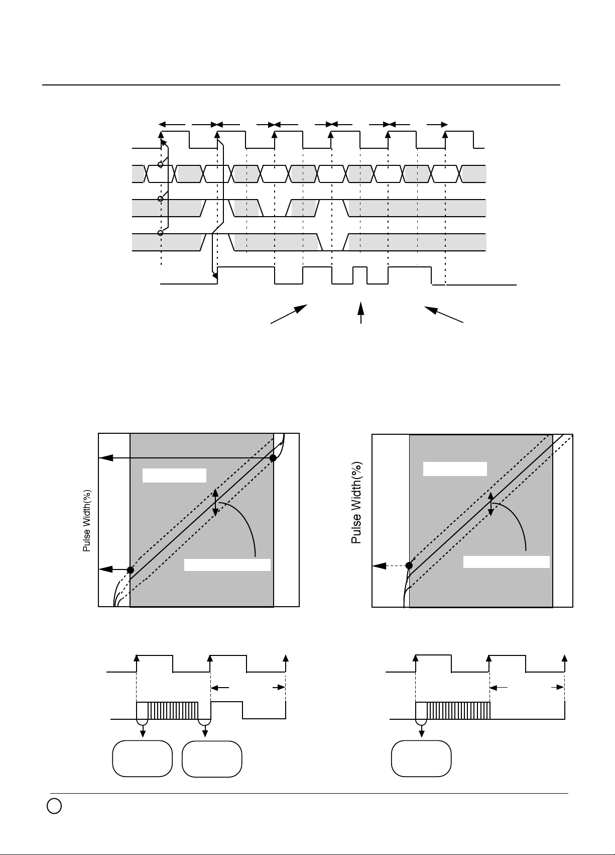
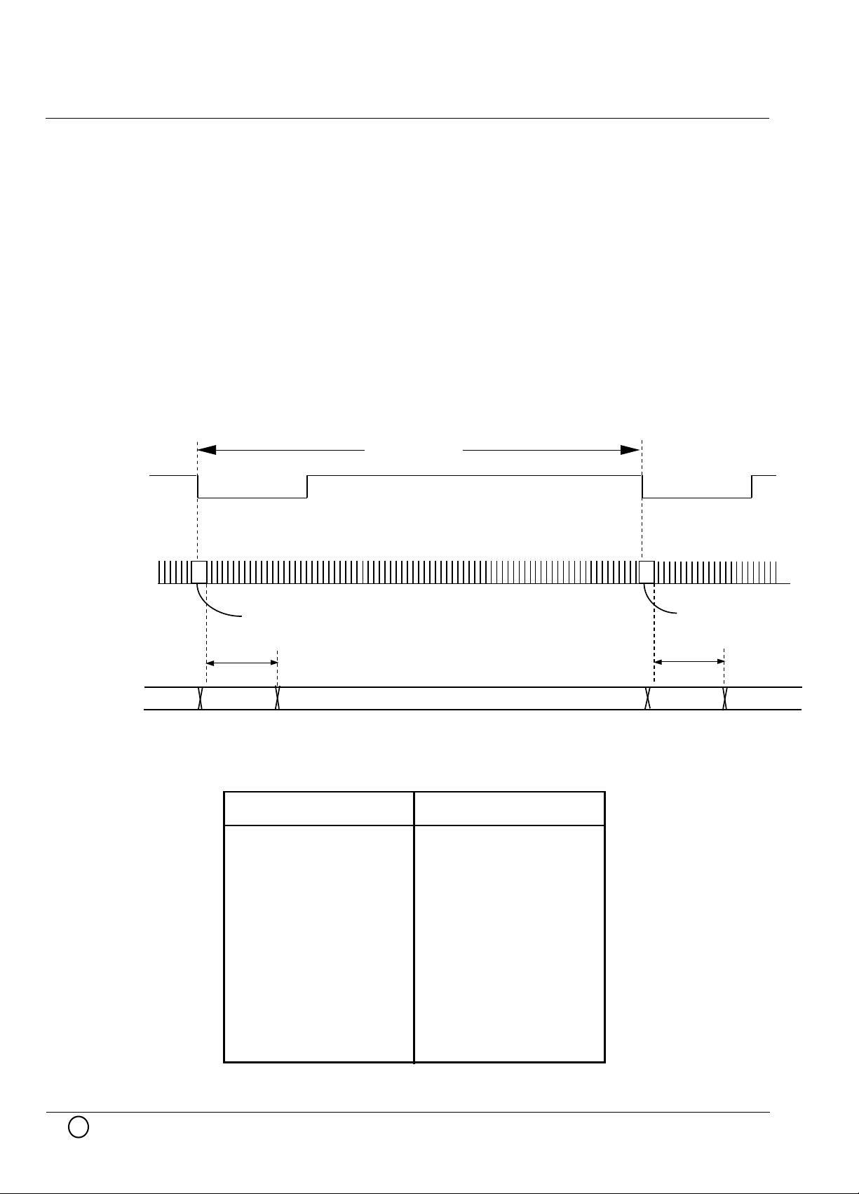
In the third cycle (N+2cycle) , DATA is 0F , SEM/DEM is "L" and LEM/TEM is "X". This means
PWMoutput width is 25% and positioning is center justify.
In the fourth cycle (N+3cycle) , DATA is 2F , SEM/DEM is "H" and LEM/TEM is "L". This
means PWMoutput width is 75% and positioning is left hand justify.
In the fifth cycle (N+4cycle) , DATA is 00 . So the CONTROL value is shown "X" . This means
the value is not important because a 0% pulse will be output for any CONTROL value.
MITSUBISHI <DIGITAL ASSP>
M66244FP
June 1998 Ver.8.0.0
FUNCTION
M66244 can control "H" width and positioning of PWM output by DATA pins (D<5:0> ) and
CONTROL pins (SEM/DEM,LEM/TEM) in each CLK period.
These inputs can be updated on the rising edge of the CLK.
Positioning the width-controlled pulse are begging , middle ,or end of the clock period.
This is accomplished through CONTROL pins (SEM/DEM,LEM/TEM)
Pulse positioning within the clock period is defined by the following CONTROL truth table.
SEM/DEM LEM/TEM Alignment
1 1 Right hand justify
1 0 Left hand justify
0 X Center justify
SEM/DEM : single edge modulation / dual edge modulation
LEM/TEM : leading edge modulation / trailing edge modulation
High Speed Monolithic Pulse Width Modulator
The diagram of page4 illustrates the output of the M66244FP with various DATA(D<5:0>) ,
CONTROL(SEM/DEM, LEM/TEM) inputs and PWM output.
This does not take into account any delays,which will explain later.
The rising edge is delayed from the leading edge of the clock, and the falling edge is delayed
from the center of the clock period.
Top line shows the clock; the second shows DATA inputs ; third shows CONTROL inputs
being updated on the rising edge of clock. The forth line shows the resulting PWM pulse with an
explanation of the second and third lines.
In the first cycle (Ncycle) , DATA is 3F . So the CONTROL value is shown as "X". This
means the value is not important because a 100% pulse will be output for any CONTROL value.
In the second cycle (N+1cycle) , DATA is 1F , SEM/DEM is "H" and LEM/TEM is "H". This
means PWMoutput width is 50% and positioning is right hand justify.
C 1998 MITSUBISHI ELECTRIC CORPORATION
(3/15)
June 1998 Ver.8.0.0
PWM OUTPUT EXAMPLE
MITSUBISHI <DIGITAL ASSP>
M66244FP
High Speed Monolithic Pulse Width Modulator
N N+1
CLK
D<0:5>
SEMDEM
LEM/TEM
PWMOUT
Right hand justify Left hand justify
PWM Pulse linearity (image figure)
N+2
N
100% 50% 25% 75% 0%
N+1 N+2
N+3
2F3F 1F 0F 00 3F
N+4
N+3
Center hand justify
Minimum
"L" Pulse
Width
Minimum
"H" Pulse
Width
CLK
PWMOUT
100
0
(1) In case of next pulse is "H" (2) In case of next pulse is "L"
100
Liner region
Change of linearity
Minimum
"H" Pulse
Width
Liner region
Change of linearity
0
0
"L"
Code (Dec)
"H"
Next Pulse
63
0
"L"
Code (Dec)
Next Pulse
63
"L"
Minimum
"H" Pulse
Width
C 1998 MITSUBISHI ELECTRIC CORPORATION
Minimum
"L" Pulse
Width
Minimum
"H" Pulse
Width
(4/15)
MITSUBISHI <DIGITAL ASSP>
M66244FP
June 1998 Ver.8.0.0
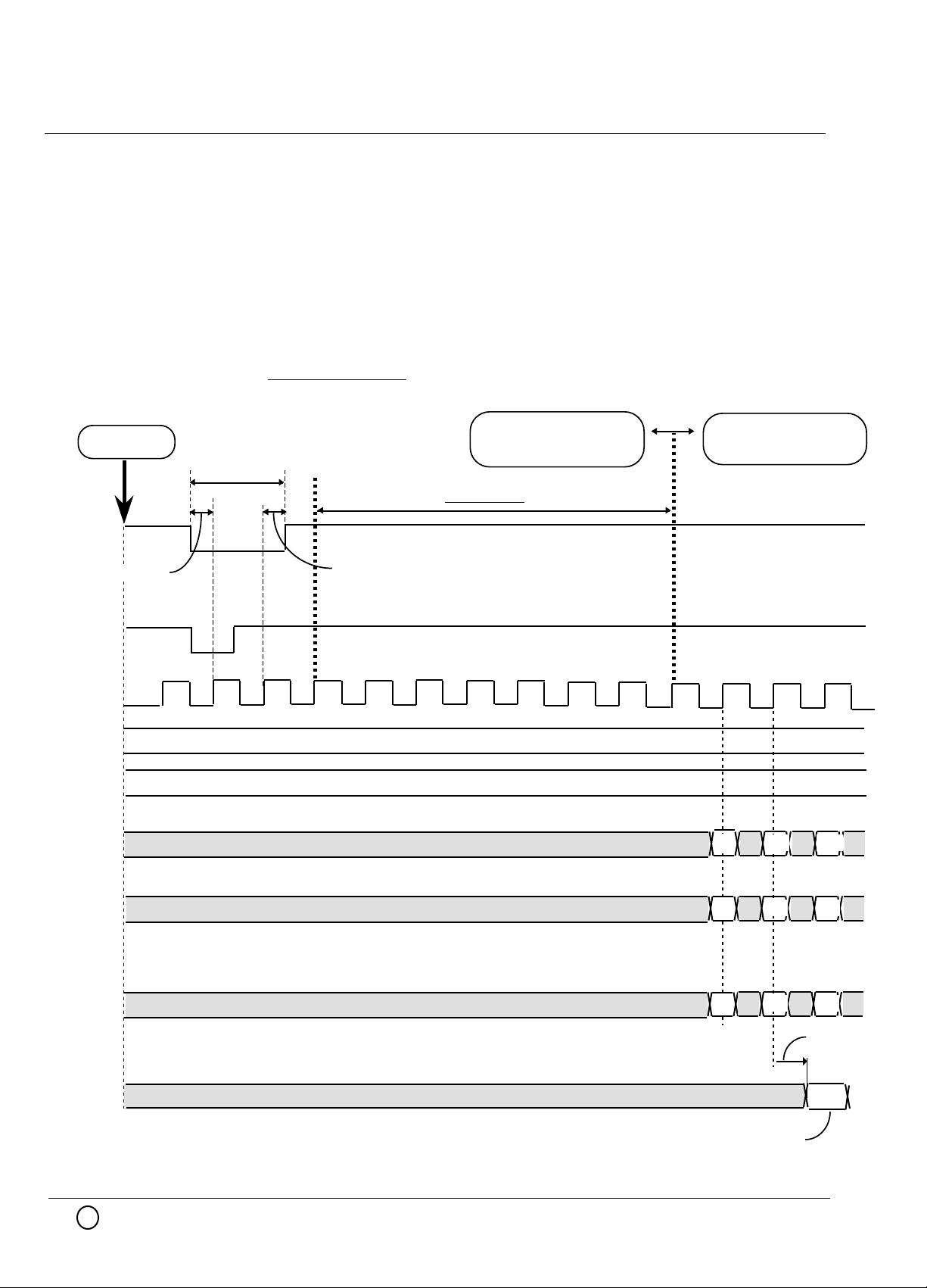
OPERATING TIMING BETWEEN POWER ON TO NORMAL OPERATION
After Power on, it needs following oerations before start normal operation.
(1) Set the value of FRANGE1 and FRANGE2 depends on operation ferequency. (Refer to page 9)
(2) Input CLK same as normal operarion frequency.
(3) Reset operarion using RESET (31pin) and TRST (3pin) .
(reset to initial state of internal logic and BSR)
(4) CLK continue to input during 100msec.
High Speed Monolithic Pulse Width Modulator
Power ON
RESET
tsu(RESET)
TRST
CLK
FRANGE1
FRANGE2
D<5:0>
reset cycle
set up period
of internal circuit
100msec
th(RESET)
Fixed value determined page9
Fixed value determined page9
normal operation
period
n
n+2n+1
SEM/DEM
LEM/TEM
PWMOUT
Note: The reset cycle requires a minimum of two cycles.
C 1998 MITSUBISHI ELECTRIC CORPORATION
(5/15)
n
n
N cycle
output
n+1
n+2n+1
n+2
td(PWM)
n

MITSUBISHI <DIGITAL ASSP>
M66244FP
June 1998 Ver.8.0.0
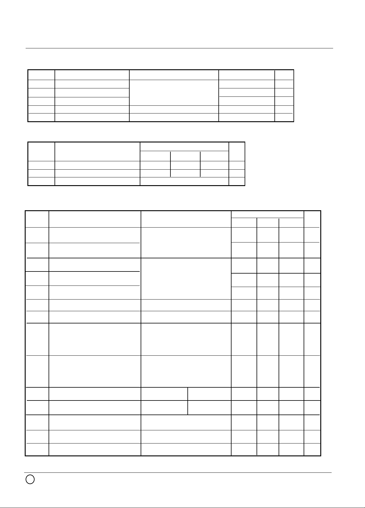
OPERATING TIMING EXAMPLE
DATA(D<0:5>) and CONTROL(SEM/DEM,LEM/TEM) are written to the latching circuit at the
first rise edge of CLK. PWMOUT is outputted at the next edge of CLK. A propagation delay
exists between the CLK and PWMOUT pulse. The minimum propagation delay can be observed
when alternating between codes 00(H) and 3F(H).
In the following diagram, when SET is "H" , PWM output is "H" , when SET is "L" , PWMOUT is
determined correspond to D<5:0>. The function of SET is direct set, so when the rise edge of
CLK and SET are entered at the same time PWMOUT will be "H" .
SET
High Speed Monolithic Pulse Width Modulator
tw(SET)
CLK
D<5:0>
SEM/DEM
LEM/TEM
tw(CLK)
N cycle
tsu(D) th(D)
tsu(SD)
tsu(LT) th(LT)
th(SD)
N+1 cycle
td(PWM)
N+2 cycle
n+2n+1n
n+2n+1n
n+2n+1n
td(SET)
N+3 cycle
n+3
n+3
n+3
N+4 cycle
n+3
n+3
n+3
td(PWM)
td(SET)
PWMOUT
C 1998 MITSUBISHI ELECTRIC CORPORATION
n
N
cycle output
(6/15)
"H"
n+3
N+3
cycle output
MITSUBISHI <DIGITAL ASSP>
June 1998 Ver.8.0.0
High Speed Monolithic Pulse Width Modulator
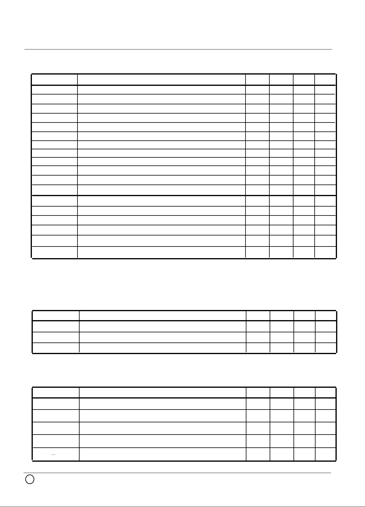
TIMING CONDITIONS (Ta=0~ 70˚C,Vcc=3.3V±5%, GND=0V)
M66244FP
Symbol Parameter
tw(CLK)
duty(CLK)
tsu(RESET)
th(RESET)
tw(SET)
tsu(D)
th(D)
tsu(SD)
th(SD)
tsu(LT)
th(LT)
tr / tf Input pulse rise / fall time
tw(TCK)
tsu(TDI)
th(TDI)
tsu(TMS)
th(TMS)
tw(TRST)
Clock cycle
Clock duty
RESET setup time to CLK
RESET hold time to CLK
SET pulse width
Input data setup time to CLK
Input data hold time to CLK
SEM/DEM setup time to CLK
SEM/DEM hold time to CLK
LEM/TEM setup time to CLK
LEM/TEM hold time to CLK
TCK cycle
TDI setup time to CLK
TDI hold time to CLK
TMS setup time to CLK
TMS hold time to CLK
TRST pulse width
14
14
50
10
10
10
10
20
Typ.
6
6
6
6
6
6
6
6
Max.
±7
22
2
UnitMin.
ns
%
ns
ns
ns
ns
ns
ns
ns
ns
ns
ns
ns
ns
ns
ns
ns
ns
SWITCHING CHARACTERISTICS (Ta=0~ 70˚C,Vcc=3.3V±5%, GND=0V)
Symbol Parameter
td (PWM) PWM output access time ns
td (SET)
td (TDO)
TDO access time
Typ.
Max.
40
20
40
OUTPUT PULSE LINEARITY (Ta=0~ 70˚C,Vcc=3.3V±5%, GND=0V)
Symbol
DLV
DLT
DLW
Pw+(min)
Pw (max)
Parameter
Differential linearity by voltage change
Differential linearity by temperature change
Differential linearity by wafer lot change
Minimum "H" pulse width
Minimum "L" pulse width
(@CL=10pF)
(@CL=10pF)
4
4
Typ.
Max.
4
4
4
UnitMin.
ns"H" output access time
ns
UnitMin.
%
%
%
ns
ns
C 1998 MITSUBISHI ELECTRIC CORPORATION
(7/15)
positive going threshold voltage
for schmitt type input
June 1998 Ver.8.0.0
High Speed Monolithic Pulse Width Modulator
ABSOLUTE MAXIMUM RATINGS (Ta=0~70˚C unless otherwise noted)
MITSUBISHI <DIGITAL ASSP>
M66244FP
Symbol
Vcc
VI
Vo
Pd
Tstg
Parameter
Supply voltage
Input voltage
Output voltage
Maximum power dissipation
Storage temperature
Conditions
A value based GND pin
Ta = 70 ˚C
Ratings
-0.3~+4.6
-0.3~VCC+0.3
-0.3~VCC+0.3
414
-55~150
Unit
V
V
V
mW
˚C
RECOMMENDED OPERATING CONDITIONS
Symbol
Vcc
GND
Topr
Parameter
Supply voltage
Supply voltage
Operating ambient temperature
Min. Typ. Max.
3.15 3.45
Limits
3.3
0
0~70
Unit
V
V
˚C
ELECTRICAL CHARACTERISTICS (Ta=0~70˚C, Vcc=3.3V±5%,GND=0V unless otherwise noted)
0.5
2.0
Limits
Typ.
0.75
Max.
1.65
2.41.4
Symbol Parameter
VIH
VIL
VT-
VT+
VH
VOH
"H" Input voltage
for normal type input
"L" Input voltage
for normal type input
Negative going threshold voltage
for schmitt type input
Hysteresis
for schmitt type input
"H" Output voltage
Conditions
D0~D5, LEM/TEM ,LS
SEM//DEM, CLK, SET,
FRANGE1, FRANGE2
TCK, TRST, RESET
Vcc=3.3V
IOH=-2mA
Min.
Vcc x 0.8
0.8
Unit
V
V
V
V
V
V
VOL
IIH
IIL
IOZH
IOZL
Icc
CI Input capacitance
CO
"L" Output voltage
"H" Input current
"L" Input current
Off state "H" output current
Off state "L" output current
Operating mean
current dissipation
Off state output capacitance
Note 1 : under consideration
C 1998 MITSUBISHI ELECTRIC CORPORATION
IOL=2mA
VI=Vcc
VI=GND
Vo=Vcc
Vo=GND
f=72MHz , CL=10pF
f=1MHz
f=1MHz
(8/15)
TDO
TDO
0.55
10
-10
10
-10
120
10
15
V
µA
µA
µA
µA
mA
pF
pF

MITSUBISHI <DIGITAL ASSP>
M66244FP
June 1998 Ver.8.0.0
SETTING OF OPERATING FREQUENCY RANGE
M66244FP can operate between 45MHz to 72MHz of clock frequency, it needs to set the value
of the FRANGE1 and FRANGE2 correspond to operating frequency.
High Speed Monolithic Pulse Width Modulator
Frequency range
45MHz~50MHz
50MHz~60MHz
60MHz~72MHz
FRANGE1 FRANGE2
L
H
H
H
L
H
TIMING of PROPAGATION DELAY and THRESHOLD VOLTAGE of PULSE WIDTH
3.0V
0V
VOH
VOL
CLK
PWMOUT
1.3V
td(PWM)
1.3V
tw(PWM)
SET
PWMOUT
NOTE : OUTPUT LOAD 10pF
C 1998 MITSUBISHI ELECTRIC CORPORATION
1.3V
td(SET)
1.3V
(9/15)
"H"
3.0V
0V
VOH
VOL
MITSUBISHI <DIGITAL ASSP>
M66244FP
June 1998 Ver.8.0.0
Solution for clock period is shifted
In the printer or copier system, there are some possibility that clock period is shifted because
beam detect signal generates at the beginning of each pass across the paper.
If clock period is shifted one time, PWMOUT will be invalid. It needs long time to recover valid
PWMOUT after previous clock period inputted.
To settle above problem, beam detect signal take in to LS (16 pin) of M66244FP.
For this, It can recover valid PWMOUT within 4usec after previous clock period inputted.
1 line sequence
High Speed Monolithic Pulse Width Modulator
Beam-detect
PWM clock
PWMOUT
4 usec
valid invalid
clock stopped time (ns)
Phase shifted clock
valid
Example of operating timing using LS function
recovery time(ns)
20
40
60
80
100
200
400
600
800
1000
2000
4000
1000
1000
2000
4000
7000
10000
14000
17000
20000
23000
30000
40000
Phase shifted clock
4 usec
invalid
valid
recovery time that not using LS function
C 1998 MITSUBISHI ELECTRIC CORPORATION
(10/15)

MITSUBISHI <DIGITAL ASSP>
June 1998 Ver.8.0.0
M66244FP
High Speed Monolithic Pulse Width Modulator
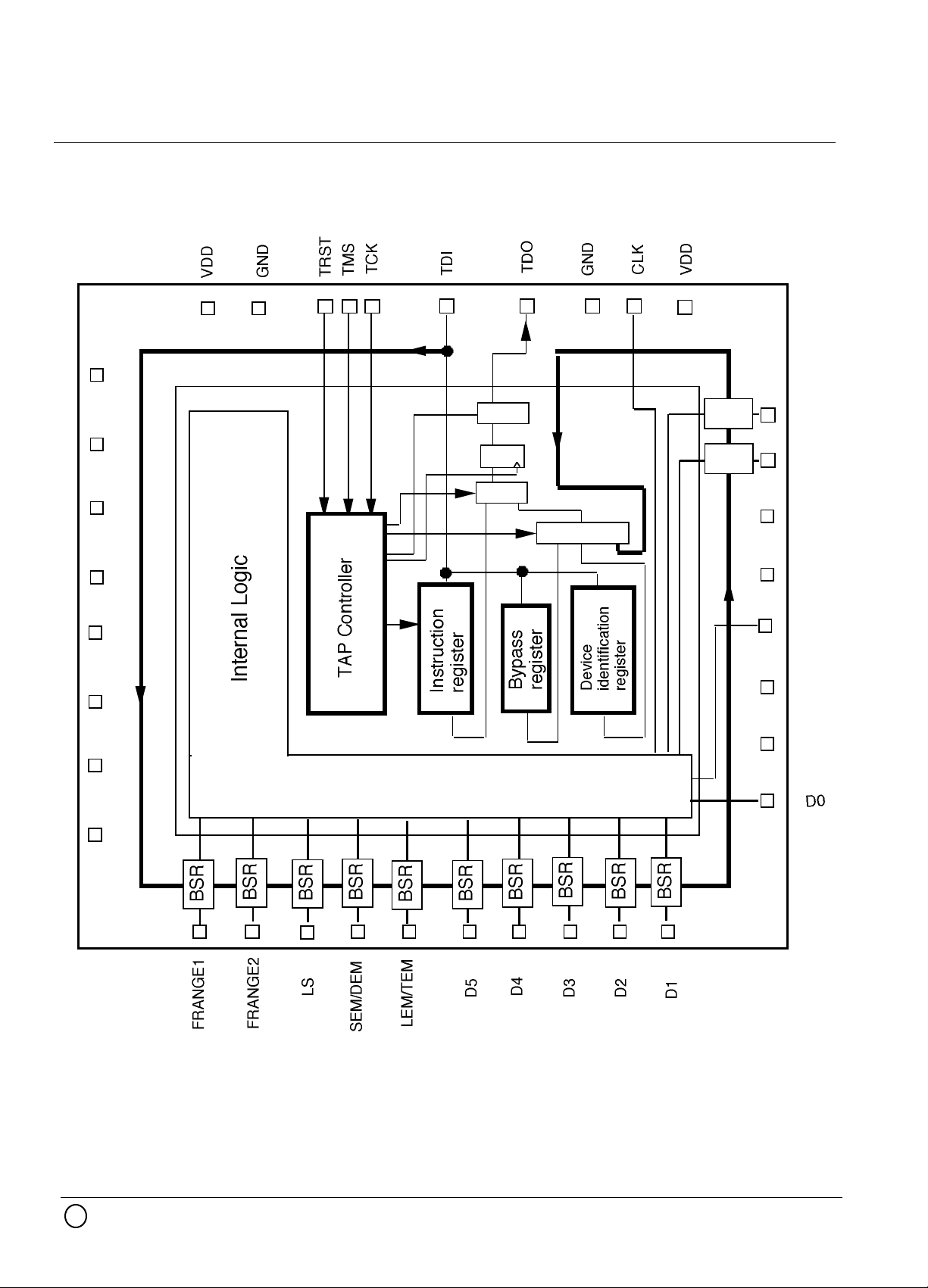
TEST CIRCUIT DESCRIPTION (JTAG)
GENERAL DESCRIPTION
The Test Access Port conforms with the IEEE standard 1149.1.
This standard defines a test access port and boundary-scan architecture for digital integrated
circuits.
The facilities defined by the standard seek to provide a solution to the problem of testing
assembled printed circuit boards and other products based on highly complex digital
integrated circuits and high-density surface-mounting assembly techniques. They also
provide a means of accessing and controlling design-for-test features build into digital
integrated circuits themselves.
PIN DESCRIPTION
TCK,TMS,TDI,TRST,TDO are used in this test operation.
•Test Clock Input (TCK)
TCK provides the clock for the test logic defined by this standard. Stored-state devices
contained in the test logic retain their state indefinitely when the signal applied to TCK is
stopped at 0.
•Test Mode Select Input (TMS)
The signal received at TMS is decoded by the TAP controlled to control test operation.
The signal presented at TMS is sampled by the test logic on the rising edge of TCK.
•Test Data Input (TDI)
Serial test instructions and data are received by the test logic at TDI.
The signal presented at TDI is sampled by the test logic on the rising edge of TCK.
•Test Reset Input (TRST)
The TRST input provides for asynchronous initialization of the TAP controller.
If TRST is included in the TAP, then the TAPcontroller is asynchronously reset to the TestLogic-Reset controller state when a logic 0 is applied to TRST.
•Test Data Input (TDO)
TDO is a serial output for test instructions and data from the test logic defined in this
standard.
Changes in the state of the signal driven through TDO occur only on the falling edge of
TCK. The TDO driver is set to its inactive drive state except when the scanning of data is in
progress.
C 1998 MITSUBISHI ELECTRIC CORPORATION
(11/15)
MITSUBISHI <DIGITAL ASSP>
M66244FP
June 1998 Ver.8.0.0
BLOCK DIAGRAM OF TEST CIRCUIT
3
GND
VDD
GND
5
6
7
8
4
High Speed Monolithic Pulse Width Modulator
2
361
33
3435
32
BSR
BSR
29
31
30
RESET
SET
VDD
VDD
GND
VDD
GND
VDD
10
11
12
13
9
14 15
16
17
18 19 20 21 22
23
28
27
26
25
24
GND
PWMOUT
VDD
GND
NOTE1 : BSR routing order = FRANGE1→FRANGE2→LS →SEMDEM→
LEMTEM→D5→D4→D3→D2→D1→D0 →SET →RESET
NOTE2 : CLK(33pin) and PWMOUT(27pin) do not have BSR.
C 1998 MITSUBISHI ELECTRIC CORPORATION
(12/15)

MITSUBISHI <DIGITAL ASSP>
M66244FP
June 1998 Ver.8.0.0
TAP CONTROLLER DESCRIPTION
The TAP controller is a synchronous finite state machine that responds to change at the
TMS and TCK signals of the TAP and controls the sequence of operations of the circuitry
defined by this standard.
The state diagram for the TAP controller is shown in following figure.
All state transitions of the TAP controller occur on the value of TMS at the time of a rising
edge of TCK.
High Speed Monolithic Pulse Width Modulator
C 1998 MITSUBISHI ELECTRIC CORPORATION
(13/15)

MITSUBISHI <DIGITAL ASSP>
length serial path between the TDI and the TDO pins of a M66244FP when no test operation of
M66244FP is required.
This allows more rapid movement of test data to and from other components on a board that
are required to perform test operations.
The BYPASS instruction select the bypass register to be connected for serial access between
TDI and TDO in the Shift-DR controller state.
M66244FP
June 1998 Ver.8.0.0
INSTRUCTION DESCRIPTION
INSTRUCTION SET
Instruction Code (Binary)
EXTEST
IDCODE
SAMPLE/PRELAOD
BYPASS
000
001
010
111
High Speed Monolithic Pulse Width Modulator
Selected TDR
BSR (Boundary Scan Register)
DIR (Device Identification Register)
BSR
BPR (Bypass Register)
EXTEST INSTRUCTION
EXTEST instruction allows testing of off-cihp circuitry and board level interconnections. Data
would typically be loaded onto the latched parallel outputs of boundary-scan shift-register
stages using the SAMPLE/PRELOAD instruction prior to selection of the EXTEST instruction.
The EXTEST instruction select only the BSR(Boundary-scan register) to be connected for
serial access between TDI and TDO in the Shift-DR controller state.
When the EXTEST instruction is selected, the state of all signals received at system input
pins are loaded into the boundary-scan register on the rising edge of TCK in the Capture-DR
controller state.
PWMOUT pin does not have BSR, so PWMOUT pin can not test interconnection to board
using the EXTEST instruction.
BYPASS INSTRUCTION
The bypass register contains a single shift-register stage and is used to provided a minimum-
C 1998 MITSUBISHI ELECTRIC CORPORATION
(14/15)

MITSUBISHI <DIGITAL ASSP>
M66244FP
June 1998 Ver.8.0.0
SAMPLE/PRELOAD INSTRUCTION
The SAMPLE/PRELOAD instruction allows a snapshot of normal operation of the component
to the taken and examined. It also allows data values to be loaded onto the latched parallel
outputs of the boundary-scan shift register prior to selection of the other boundary-scan test
instruction.
The SAMPLE/PRELOAD instruction select only the boundary-scan register to be connected
for serial access between TDI and TDO in the Shift-DR controller state.
When SAMPLE/PRELOAD instruction is selected, the state of all signals flowing through
system pins are loaded into the register on the rising edge of TCK in the Capture-DR controller
state.
When SAMPLE/PRELOAD instruction is selected, parallel output registers/latches included in
boundary-scan register cells load the data held associated shift-register stage on the falling
edge of TCK in the Update-DR controller state.
High Speed Monolithic Pulse Width Modulator
IDCOAD INSTRUCTION
Use of the device identification register allows a code to be serially read from the component
that shows:
(1)The version number for the part
(2)The part number
(3)The manufacturer's identity
The IDCODE instruction select only the device identification register to be connected for serial
access between TDI and TDO in the Shift-DR controller state.
When the IDCODE instruction is selected, the vendor identification code is loaded into the
device identification register on the rising edge of TCK following entry into Capture-DR
controller state.
ID code of M66244FP is as follow;
Version
(4bit)
Part num.
(16bit)
bit num.
code
bit num.
code
31 30 29 28
0 0 0 0
27 26 25 24 23 22 21 20 19 18 17 16 15 14 13 12
0 0 0 1 1 0 0 0 0 1 1 0 0 1 0 0
binary code
of "6244"
Manufacture num.
(11bit)
LSB
(4bit)
C 1998 MITSUBISHI ELECTRIC CORPORATION
bit num.
code
bit num.
code
11 10 9 8 7 6 5 4 3 2 1
0 0 0 0 0 0 1 1 1 0 0
0
1
JEDEC code
of MITSUBISHI
fixed value
(15/15)
 Loading...