Page 1

MITSUBISHI 〈DIGITAL ASSP〉
MITSUBISHI 〈DIGITAL ASSP〉
DESCRIPTION
M66236 is produced using the silicon gate CMOS process. It
is able to output clock input signal in sync with optional external trigger input signal.
It features excellent synchronizing precision (jitter) over a
wide frequency band range.
FEATURES
• 5V single power supply (5V ±5%)
• Frequency band: 12 ~ 25MHz
• Synchronizing precision (jitter): ±5ns
• Output types
(1) Output of the same frequency as input clock, and its in-
version
(2) 1/2 divider clock output and its inversion
(3) One-shot pulse output
(4) Continuous clock output
• Noise in the positive direction to trigger input is removed by
built-in noise killer circuit
M66236FP
STANDARD CLOCK GENERATOR
STANDARD CLOCK GENERATOR
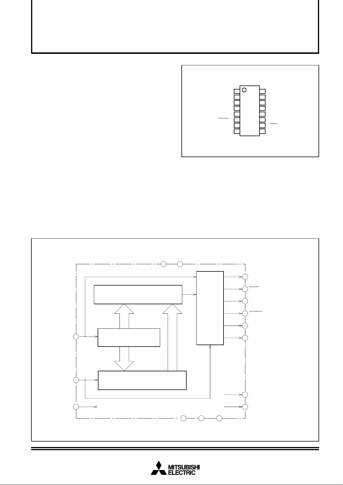
PIN CONFIGURATION (TOP VIEW)
CLOCK INPUT
TEST INPUT
TEST OUTPUT
ONE-SHOT PULSE
OUTPUT
1/2 DIVIDER SYNC CLOCK
INVERTED OUTPUT
1/2 DIVIDER SYNC
CLOCK OUTPUT
Note: Keep test pins (TEST 1 to 3) open.
CLK IN
TEST1
TEST2
PULSE
CKO/2
CKO/2
GND
GND
2
→
3
←
4
←
5
6
←
7
←
8
1
→
Outline 16P2N-A
16
M66236FP
15
14
13
12
11
10
9
M66236FP
VCC
TEST3
→
TEST OUTPUT
GND
TR
←
TRIGGER INPUT
VCC
CKO
→
SYNC CLOCK OUTPUT
SYNC CLOCK
CKO
→
INVERTED OUTPUT
CONTINUOUS
CNTCK
→
CLOCK OUTPUT
APPLICATION
Clock phase control for horizontal synchronization
BLOCK DIAGRAM
SYNC CLOCK SELECTOR CIRCUIT
CLOCK
INPUT
CLK IN
1
DELAY CLOCK
GENERATION CIRCUIT
V
CCVCC
12 16
SYNC CLOCK GENERATION CIRCUIT
11
10
7
6
9
4
SYNC CLOCK
CKO
OUTPUT
SYNC CLOCK
CKO
INVERTED OUTPUT
1/2 DIVIDER SYNC
CKO/2
CLOCK OUTPUT
1/2 DIVIDER SYNC
CKO/2
CLOCK INVERTED OUTPUT
CONTINUOUS
CNTCK
CLOCK OUTPUT
ONE-SHOT
PULSE
PULSE OUTPUT
TRIGGER
INPUT
TEST
INPUT
TR
TEST1
13
PHASE DETECTION CIRCUIT
3
TEST2 TEST OUTPUT
2
85
14
GNDGND
GND
TEST3 TEST OUTPUT
15
1
Page 2

MITSUBISHI 〈DIGITAL ASSP〉
M66236FP
STANDARD CLOCK GENERATOR
FUNCTION
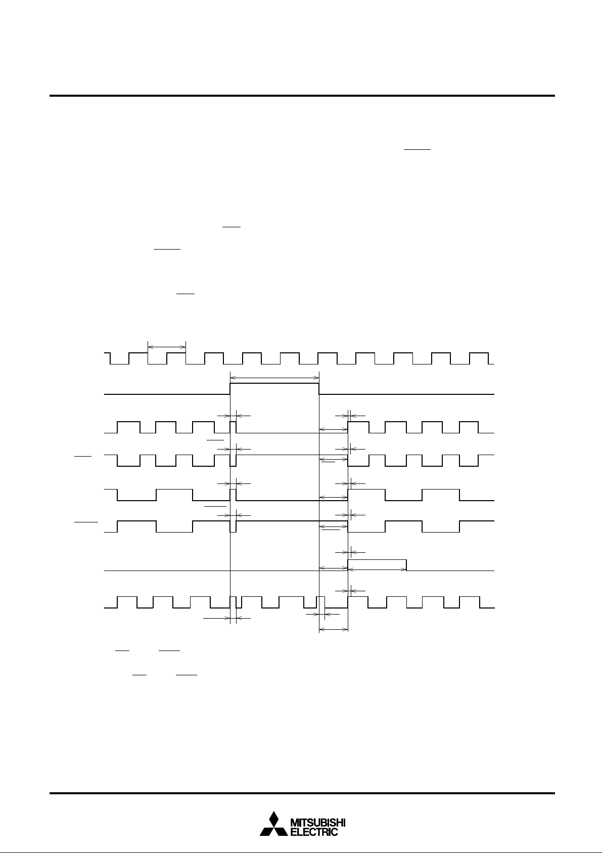
M66236 standard clock generator outputs clock input signal,
which is input to CLK IN, synchronously with optional trigger
signal, which is input to TR.
Sync clock output timing is determined by trigger input signal
fall edge. Time-lag between trigger input signal fall edge and
sync clock output equals the sum of clock input signal “L”
pulse width and M66236 internal delay. Variation in this lag
(∆t) is ±5ns, ensuring excellent synchronizing accuracy.
There are six types of outputs: synchronous clock output
(CKO), synchronous clock inverted output (CKO), 1/2 divider
synchronous clock output (CKO/2), 1/2 divider synchronous
clock inverted output (CKO/2), one-shot pulse output
(PULSE) and continuous clock output (CNTCK).
From synchronous clock output (CKO), sync clock of the
same frequency as clock input signal is output. From synchronous clock inverted output (CKO), inverted signal of sync
1/f
IN
CLK IN
t
w(TR)
TR
t
sp(CKO)
CKO
t
sp(CKO)
CKO
t
sp(CKO/2)
CKO/2
t
sp(CKO/2)
CKO/2
PULSE
CNTCK
t
CH
clock output from CKO is output. From 1/2 divider synchronous clock output (CKO/2), 1/2 divider signal of sync clock
output from CKO is output. From 1/2 divider synchronous
clock inverted output (CKO/2), inverted signal of that output
from CKO/2 is output.
From one-shot pulse output (PULSE), one-shot pulse which
is almost equal to two cycles of clock input signal is output
after trigger input signal falls. From continuous clock output
(CNTCK), sync clock is output when trigger input signal is on
“L” level; when trigger input signal is on “H” level, clock input
signal, which is input to CLK IN, is output.
All these outputs but continuous clock output are suspended
when trigger input signal is on “H” level: Synchronous clock
output, 1/2 divider synchronous clock output and one-shot
pulse output stay on “L” level, and synchronous clock inverted
output and 1/2 divider synchronous clock inverted output stay
on “H” level.
V
0V
3V
0V
∆t
t
t
t
t
t
t
CL
ss(CKO)
ss(CKO)
ss(CKO/2)
ss(CKO/2)
ss(PULSE)
∆t
∆t
∆t
∆t
t
w(PULSE)
∆t
t
ss(CNTCK)
V
V
V
V
V
V
V
V
V
V
V
V
CC
OH
OL
OH
OL
OH
OL
OH
OL
OH
OL
OH
OL
Note 1:tSS (CKO, CKO, CKO/2, CKO/2 and PULSE) equals the sum of input clock “L” width and α . Value α refers to internal delay in M66236. Under envi-
ronment where temperature and V
chronizing precision (jitter)].
Note 2:Outputs (CKO, CKO, CKO/2, CKO/2 PULSE and CNTCK) are unknown until trigger input TR reaches “H” level for the first time after power-on.
CC do not change, value α and tss are kept constant. Dispersion of tss under such conditions is defined as ∆t [syn-
2
Page 3

After Power-on Procedure
After power-on, M66236 status is unknown till the trigger input being set to the “H” level.
To get a accurate sync clock output, please keep a following
procedure.
V
CC
TR
CLK IN
CKO
MITSUBISHI 〈DIGITAL ASSP〉
M66236FP
STANDARD CLOCK GENERATOR
Please hold the trigger input “H” level during more than
tw(TR) after the input clock frequency being stable.
Also, in case of changing the clock input frequency(f
please keep the same procedure.
IN),
tsp
Input clock frequency is stable
tw (TR)
3
Page 4

ABSOLUTE MAXIMUM RATINGS
Parameter
Conditions
When mounted
VCC
VI
VO
Pd
Tstg
Symbol
Supply voltage
Input voltage
Output voltage
Power dissipation
Storage temperature
RECOMMENDED OPERATING CONDITIONS (Ta = 0 ~ 70°C unless otherwise noted)
Limits
Typ
0
0
0
VCC
GND
VI
VO
Topr
Symbol
Parameter
Supply voltage
Supply voltage
Input voltage
Output voltage
Operating temperature
Min
4.75
MITSUBISHI 〈DIGITAL ASSP〉
M66236FP
STANDARD CLOCK GENERATOR
Ratings
–0.5 ~ +7.0
–0.5 ~ VCC + 0.5
–0.5 ~ VCC + 0.5
600
–65 ~ 150
70
Unit
V
V
V
V
°C
Max
5
0
5.25
VCC
VCC
Unit
V
V
V
mW
°C
ELECTRICAL CHARACTERISTICS (Ta = 0 ~ 70°C, VCC = 5V ±5%, GND = 0V)
Test conditions
TR
CLK IN
GND = 0V , I OH = –4mA
GND = 0V, IOL = 4mA
GND = 0V,
VI = VCC or GND
GND = 0V, fIN = 25MHz,
VI = VCC or GND
GND = 0V , VI = VCC
GND = 0V, VI = 0V
VIH
VIL
VIH
VIL
VOH
VOL
ICC (s)
ICC (a)
IIH
IIL
CI
Symbol
Parameter
“H” input voltage
“L” input voltage
“H” input voltage
“L” input voltage
“H” output voltage
“L” output voltage
Supply current (static)
Supply current (active)
“H” input current
“L” input current
Input capacitance
TIMING REQUIREMENTS (Ta = 0 ~ 70°C, VCC = 5V ±5%, GND = 0V)
Test conditionsParameter
fIN
fDUTY
tw(TR)
tr
tf
Symbol
Clock input frequency
Clock input duty
Trigger input “H” pulse width
Clock input rise time
Clock input fall time
2
0.8 × V
V
CC
12
40
400
–
CC
0.8
Limits
TypMin
Limits
TypMin
0.2
Max
0.8
× V
0.55
50
65
+1
–1
10
Max
25
60
8
8
CC
Unit
V
V
V
V
V
V
µA
mA
µA
µA
pF
Unit
MHz
%
ns
ns
ns
4
Page 5

SWITCHING CHARACTERISTICS (Ta = 0 ~ 70°C, VCC = 5V ±5%, GND = 0V)
Symbol
∆t
tss(CKO)
tss(CKO)
tss(CKO/2)
tss(CKO/2)
tss(PULSE)
tss(CNTCK)
tsp(CKO)
tsp(CKO)
tsp(CKO/2)
tsp(CKO/2)
tw(PULSE)
tCH
tCL
fODUTY(CKO)
fODUTY(CKO)
Parameter
Synchronizing precision (jitter)
Sync clock output start time
Sync clock inverted output start time
1/2 divider sync clock output start time
1/2 divider sync clock inverted output start time
One-shot pulse output start time
Continuous clock output start time
Sync clock output stop time
Sync clock inverted output stop time
1/2 divider sync clock output stop time
1/2 divider sync clock inverted output stop time
One-shot pulse output width
Sync clock-Input clock switching time
Input clock-Sync clock switching time
Sync clock output duty
Sync clock inverted output duty
Test conditions
CL=15pF
MITSUBISHI 〈DIGITAL ASSP〉
M66236FP
STANDARD CLOCK GENERATOR
Limits
Min
2tp – 10
30
Typ
Max
±5
tLp + 50
tLp + 50
tLp + 50
tLp + 50
40
40
2tp + 10
40
30
70
Unit
ns
ns
ns
ns
ns
ns
ns
ns
ns
ns
ns
ns
ns
ns
%
%
•tp = 1/fIN, tLp = tp × (100 – fDUTY)/100
• Switching test waveform
Input pulse level CLK IN: 0 to VCC
TR: 0 to 3V
Input pulse rise time: 3ns
Input pulse fall time : 3ns
Criterial voltage
Input voltage CLK IN: VCC/2
TR: 1.3V
Output voltage: V
• Capacitance: C
L includes stray wiring capacitance and
CC/2 for all outputs
probe input capacitance.
TIMING DIAGRAM
TR
CKO
CKO/2
CKO
CKO/2
PULSE
CNTCK
1.3V
tss
tCL
50%
50%50%
3.0V
0V
OH
V
VOL
VOH
VOL
TEST CIRCUIT
TR
CKO
CKO/2
CKO
CKO/2
CNTCK
50Ω
1.3V
V
CC
DUT
sp
t
tCH
INPUT OUTPUT
PG
50%
50%
CL
3.0V
0V
V
OH
VOL
VOH
VOL
TR
1.3V 1.3V
t
w(TR)
3.0V
0V
PULSE
50%
t
w(PULSE)
VOH
50%
VOL
5
 Loading...