Mitsubishi M66010GP, M66010FP Datasheet

MITSUBISHI 〈DIGITAL ASSP〉
MITSUBISHI 〈DIGITAL ASSP〉
DESCRIPTION
M66010 Semiconductor Integrated Circuit inputs 24-bit data
in series and outputs it in parallel and vice versa, using shift
register function.
Equipped with 2 independent shift registers, one for serial-toparallel, the other for parallel-to-serial, this IC is able to read
serial input data into a shift register while converting data
from parallel to serial. Parallel input/output pins are set to input or output according to the bit.
The M66010 is useful in a wide range of applications, such as
MCU (micro controller unit) input/output port extension and
serial bus system data communication.
FEATURES
• Two-way serial data communication with MCU
• Serial data intake possible during parallel-to-serial conversion
• Parallel input/output switchable according to the bit
• Low power dissipation: 100µW maximum per package
CC =5V, Ta = 25˚C, quiescent)
(V
• Schmidt input (DI, CLK, S, CS)
• Open drain output (DO, D1 thru D24)
• Parallel data input and output (D1 thru D24)
• Wide operating supply voltage range (V
CC = 2V ~ 6V)
APPLICATION
MCU-related serial-parallel data conversion, serial bus control by MCU, etc.
M66010FP/GP
M66010FP/GP
24-BIT I/O EXPANDER
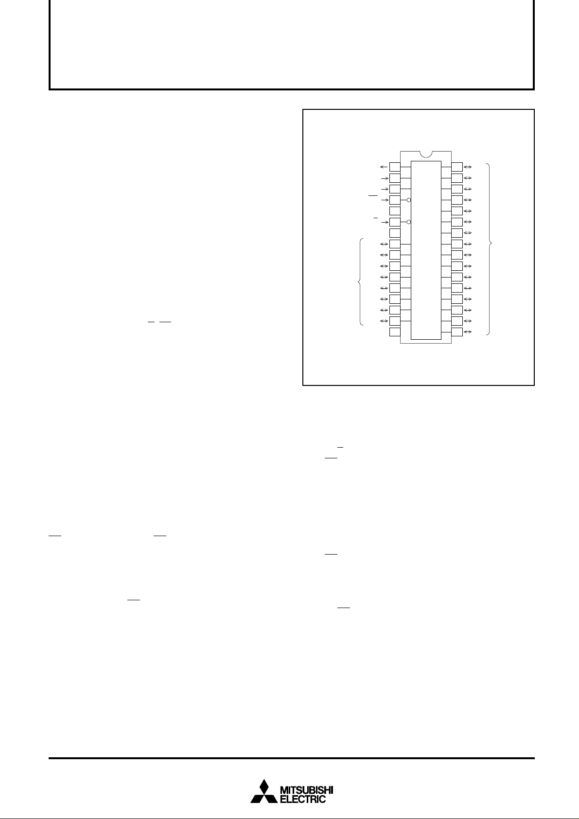
PIN CONFIGURATION (TOP VIEW)
SERIAL DATA OUTPUT
SERIAL DATA INPUT
CLOCK INPUT
CHIP SELECT INPUT
SET INPUT
PARALLEL
DATA
I/O
D0
D1
CLK
CS
V
CC
S
GND
D24
D23
D22
D21
D20
D19
D18
D17
GND
1
2
3
4
5
6
7
8
9
10
11
12
13
14
15
16
Outline
DO
DI
CLK
CS
S
D24
D23
D10
D22
D11
D21
D12
D20
D13
D19
D14
D18
D15
D17
D16
32P2W-A
D1
D2
D3
D4
D5
D6
D7
D8
D9
32P2U-B
24-BIT I/O EXPANDER
32
D1
31
D2
30
D3
29
D4
28
D5
27
D6
26
D7
PARALLEL
D8
D9
D10
D11
D12
D13
D14
D15
D16
DATA
I/O
25
24
23
22
21
20
19
18
17
FUNCTION
The M66010 is produced by using the silicon gate CMOS
(complementary metal-oxide semiconductor) technology . It is
distinguished for low power dissipation and high noise resistance.
Because two independent shift registers are built in, one for
serial-to-parallel, the other for parallel-to-serial, this IC is able
to read serial input data into a shift register while converting
parallel data into serial data.
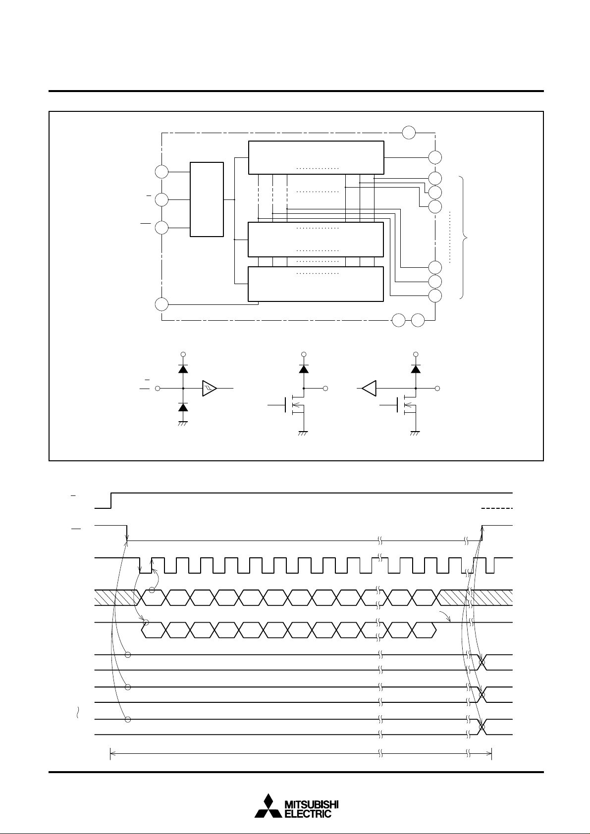
One cycle of latching 24-bit parallel data and outputing it in
series while taking in serial data from MCU is initiated by
CS’s shift from “H” to “L”. At CS fall edges, 24-bit parallel data
is latched, and output in series from pin DO synchronously
with shift clock fall edges. At shift clock rise edges, serial data
is taken in from MCU via pin DI. The data is read into shift register. The 25th and following shift clock pulses are ignored
and read-in operation is masked. The pin D0 status shifts to
high-impedance. As CS is then shifted from “L” to “H”, 24-bit
serial data taken in via pin DI is output in parallel to pins D1
thru D24. Because parallel output pins are the n-channel
open drain output type, write data “H” for pins which should
be set to input.
OPERATION
(1) When power is turned on, the status of pins D0 and D1
thru D24 is unstable. Their status turns high-impedance
when S is shifted to “L”.
(2)At CS fall edges, the status of pins D1 thru D24 is loaded
on shift register 1.
(3)At CLK fall edges, 24-bit data loaded as described above
is output in series from pin D0.
(4) At CLK rise edges, 24-bit serial data is taken in from pin
DI and written on shift register 2.
(5)The 25th and following CLK pulses are ignored, and serial
data write is discontinued. Pin D0 status turns high-impedance.
(6)At CS rise edges, data written as described in (4) is output
to pins D1 thru D24.
(7)Shift register 1 loads data added from outside as well as
AND tie data which has the same contents as data latched
by serial output latch.
(8) If the CS rises before CLK reaches the 24th bit, parallel
output latch latches data which has been written on shift
register, and output it to pins D1 thru D24.
(9)Pins D1 thru D24 are switched between input and output
according to serial data input to pin DI. Pins for which “H”
is written are set to input.
1

MITSUBISHI 〈DIGITAL ASSP〉
M66010FP/GP
24-BIT I/O EXPANDER
BLOCK DIAGRAM
CLOCK INPUT
SET INPUT
CHIP SELECT
INPUT
SERIAL DATA
INPUT
CLK
CS
CLK
CS
V
CC
5
Shift register 1
3
S
6
4
DI
2
V
S
DI
Control circuit
CC
D24 D23 D22 D3 D2 D1
Q24 Q23 Q22 Q3 Q2 Q1
Parallel output latch
D24 D23 D22 D3 D2 D1
Q24 Q23 Q22 Q3 Q2 Q1
DI
Shift register 2
V
CC
DO D1~D24
DO
7 16
GND GND
1
32
31
30
10
9
8
V
CC
SERIAL DATA
DO
OUTPUT
D1
D2
D3
D22
D23
D24
PARALLEL
DATA I/O
OPERATION TIMING CHART
(1)
S
(2)
CS
CLK
DI
DO
D1
D2
D24
1 2 3 4 5 6 7 8 9 10 23 24 25
DO1 DO2 DO3 DO4 DO5 DO6 DO7 DO8 DO9 DO23 DO24
DI1 DI2 DI3 DI4 DI5 DI6 DI7 DI8 DI9 DI23 DI24
DI1 D01
DI2 D02
DI24 D024
Input type Output type
(4)
(3)
H
L
(5)
High impedance
(6)
One cycle
2
 Loading...