


Dolby Digital Decoder
M65863FP
Product Note
April 1998
MITSUBISHI ELECTRIC CORPORATION
M65863FP is a single device. The device decodes AC-3
bitstreams into PCM audio. Dolby Digital (AC-3) is a multi-channel audio coding algorithm developed by
Dolby Laboratories, Inc.
• Decoding
1) 5.1 ch AC-3 bitstream
2) Dolby Pro Logic*1 encoded 2ch Dolby Digital (AC-3) bitstream
3) Dolby Pro Logic encoded 2ch PCM data
• All input combinations from 1 to 5.1 channels
• Output : mono 5.1 surround
• Sampling rates : 32kHz, 44.1 kHz, 48 kHz and 96 kHz (96 kHz is for linear PCM only)
• Supports a maximum bit rate of 640 kbps at a full service (up to 448 kbps when 32 kHz sampling rates)
• 2 DIR (Digital Audio Interface Receiver)/ADC input interfaces
• Serial input bitstream interface for DEMUX
• PCM output interface
Standard 3-wire DAC output interface (data,clock,LR clock), 16/18/20/24 bit DAC word size
• Supports IEC958 digital audio output for Dolby Digital (AC-3) data stream
• I2C*2 interface and clocked serial (4 line) interface for host microcontroller
• Generates audio test noise
• 2nd DSP I/F (twice higher PCM transfer rate)
• Controllable dynamic range compression
• Programmable center and surround channel delays
• Dialogue level control
• No external memory required (M65863FP doos not have memory space for surround delay)
Dolby, Dolby Digital (AC-3), and Pro Logic are registered trademarks of Dolby Laboratories Licensing Corp.
Available only to licensees of Dolby Laboratories Licensing Corporation, San Francisco, CA 94111, USA, (415) 5580200, from whom licensing and application information must be obtained.
*2 Phillips Semiconductors, "I2C bus specification",January,1992
Product Note M65863FP
April 1998 Dolby Digital Decoder
Chapter 1
Features
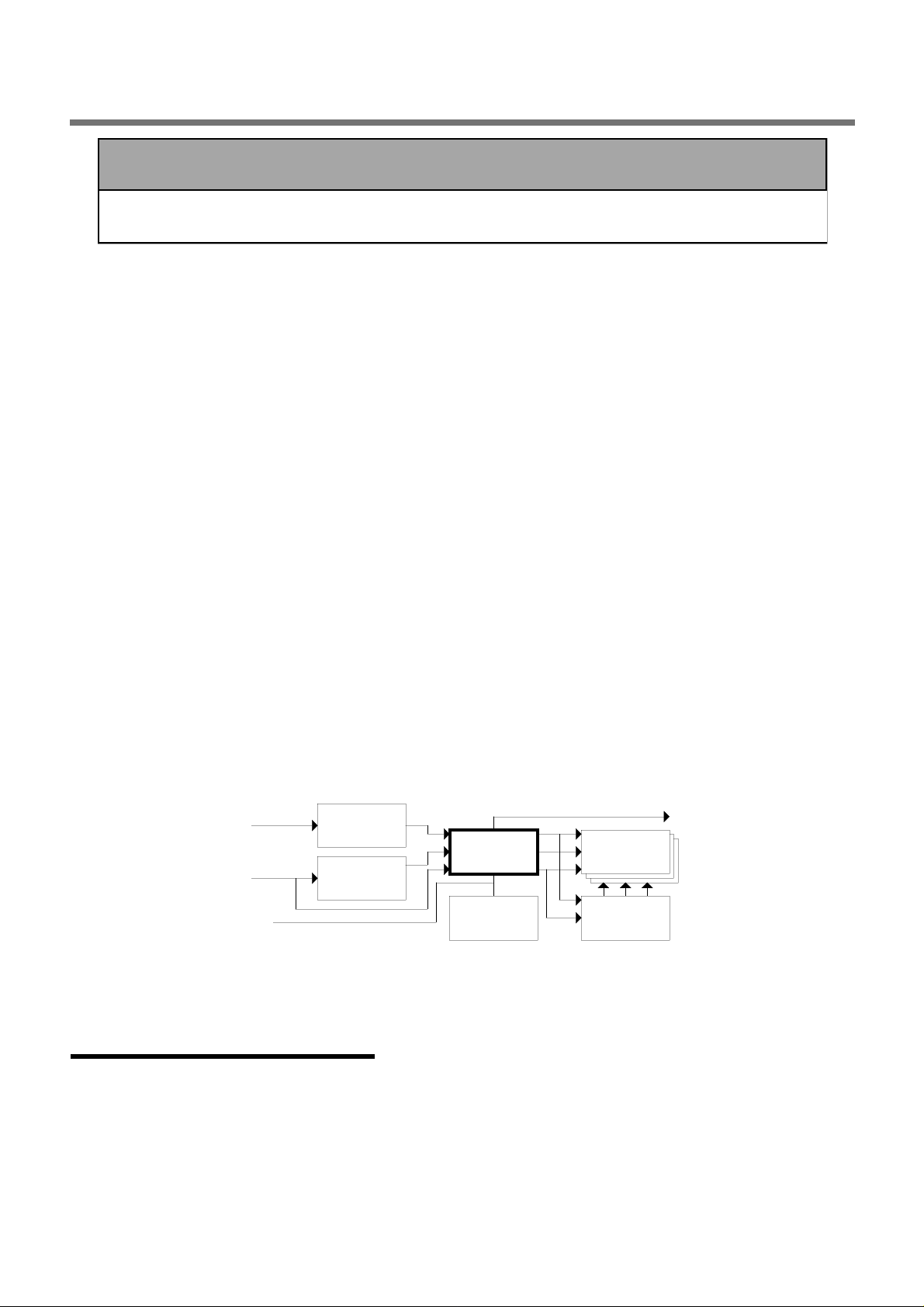
This Audio Decoder for Dolby Digital (AC-3)
Analog
IEC958
ADC
DIR
*1
M65863FP
IEC958
DAC
2
I C/Clocked serial
Figure 1.1 M65863FP Configuration Diagram (DIR I/F)
*1
MITSUBISHI ELECTRIC CORPORATION 1
MCU
DSP
Product Note M65863FP
April 1998 Dolby Digital Decoder
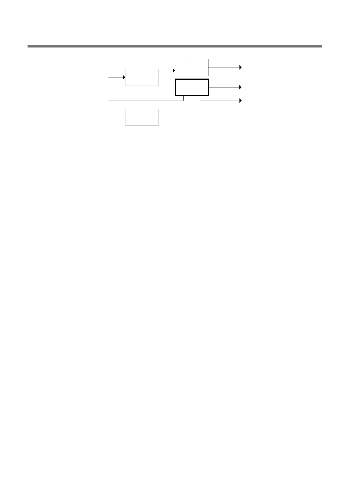
Video
Video
Decoder
DEMUX
M65863FP
Audio
IEC958
2
I C/Clocked serial
MCU
Figure 1.2 M65963FP Configuration Diagram (DEMUX I/F)
MITSUBISHI ELECTRIC CORPORATION 2
MCU Interface
Processor
Clock
DAC/DSP
Interface
Digital Audio
Interface
Audio Master Clock
Interface
Main/Sub Chip
Interface
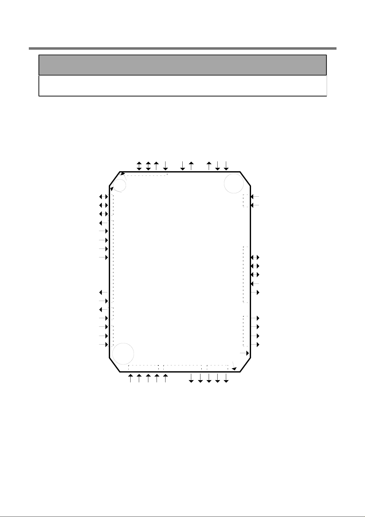
TOP VIEW
(package 68P6S-A)
VDD5V
DIRX
DOTX
GND
VDD3V
ACLK1
ADATA1
ALRCK1
GND
_AMUT
ACLKS
ADATA
ADVLDS
_ADREQ
SYNCRST
RSYCREQ
CCLK
CDATA
ASOUT
VDD5V
BCLK
LRCK
2LRCK
PLL3
PLL2
VDD3V
PLLGND
MCLKSI[1]
MCLKSI[0]
VDD5V
PLL1
PCLK
PVCO
VDD3V
PLLVCC
GND
2BCLK
DEMUX
Interface
DIR/ADC
Interface
Audio Master
Clock Selection
GND
GND
GND
PIN1
PIN68
PIN34
PIN35
Product Note M65863FP
April 1998 Dolby Digital Decoder
Chapter 2
Device Overview
The figure 2.1 show the M65863FP I/O interface.
HSCL/SCK
GND
GND
HSDA/SI
NC/_SS
NC/SO
MCUSEL
VDD5V
GND
DIRSTAT
DECSTAT
CHIPMOD
VDD5V
_RST
MITSUBISHI ELECTRIC CORPORATION 3
GND
MCLKI
VDD5V
DEMPH
ACLK2
ALRCK2
ADATA2
VDD5V
MCLKO
HMCLKO
Figure 2.1 M65863FP I/O Interface
DOLR
DOCW
GND
DOSS
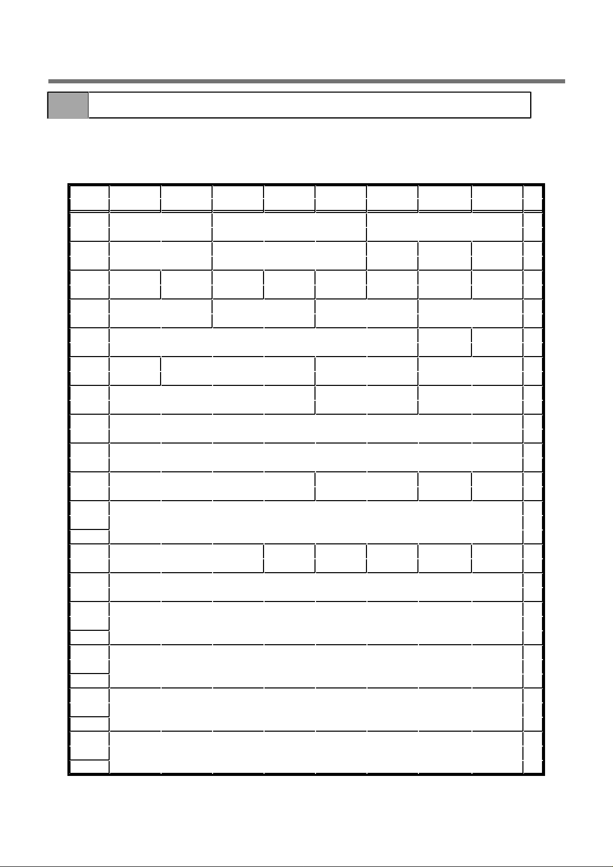
No.
Product Note M65863FP
April 1998 Dolby Digital Decoder
Chapter 3
Input/Output Pins
Table 3.1 shows input/output pins. "low active" pins are added "_" to tail of pin name (ex. _AERR).
Table 3.1 Input/Output Pins
Pin Name Pins I/O Out Voltage Description
1 VDD5V 7 - Voltage supply 5V (I/O)
2 ASOUT 1 I/O 2mA D5
3 CDATA 1 I/O 2mA D5
4 CCLK 1 I/O 2mA D5
5 RSYCREQ 1 O 2mA D5 Indication of sync word lock condition
6 SYNCRST 1 I D5 Sync world detection start signal
7 ADVLDS 1 I D5 Indication of valid data
8 ADATAS 1 I D5 Data input from DEMUX
9 ACLKS 1 I D5 Clock input from DEMUX
10 VDD3V 3 - Voltage supply 3.3V
11 GND 7 I GND
12 VDD5V
13 _ADREQ 1 O 2mA D5 Data Request for DEMUX
14 _AMUTE 1 I D5
15 DOTX 1 O 2mA D5 Digital audio interface IEC958 output
16 DIRX 1 I D5 Digital audio interface IEC958 input
17 ALRCK1 1 I D5 L/R clock from DIR/ADC
18 ACLK1 1 I D5 Data from DIR
19 ADATA1 1 I D5 Bit clock from DIR/ADC
20 GND
21 VDD5V
22 DEMPH 1 I D5 De-emphasis control
23 ALRCK2 1 I D5 L/R clock from DIR/ADC
24 ACLK2 1 I D5 Bit clock from DIR
25 ADATA2 1 I D5 Data from DIR
26 MCLKI 1 I D5 Audio master clock input
27 GND
28 VDD5V
29 MCLKO 1 I D5 Audio master clock output
30 HMCLKO 1 I D5 Audio master clock output (1/2MCLKI)
31 DOLR 1 O 2mA D5 PCM output for L ch and R ch
32 DOCW 1 O 2mA D5 PCM output for C channel SW ch
33 DOSS 1 O 2mA D5 PCM output for SL ch and SR ch
Indication of audio data output timing (main chip output / sub chip
input)
Dynamic range compression data input from sub chip / output to main
chip
Dynamic range compression data transfer clock input from sub chip /
output to main chip
Mute sound0 (0 : Mute ON, 1 : Mute OFF)
MITSUBISHI ELECTRIC CORPORATION 4
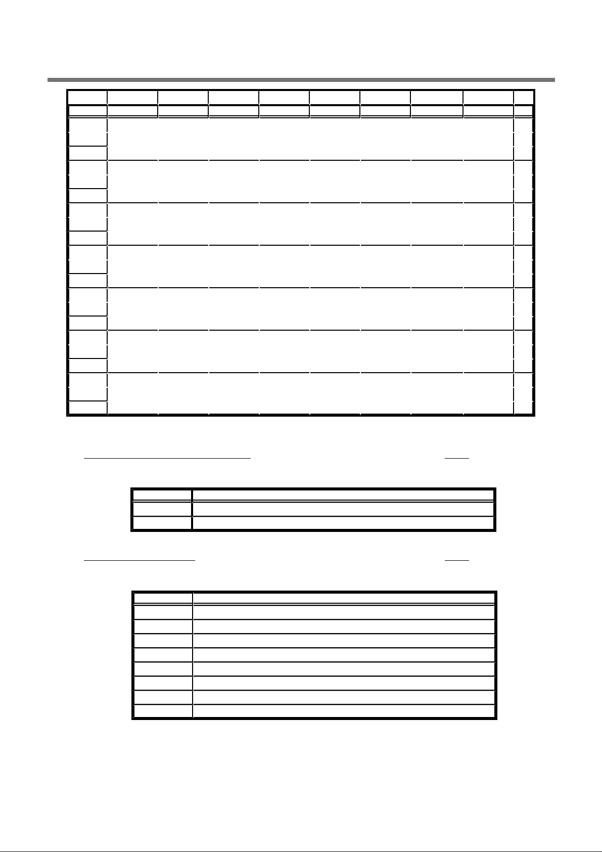
No.
Product Note M65863FP
April 1998 Dolby Digital Decoder
Pin Name Pins I/O Out Voltage Description
34 GND
35 VDD5V
36 BCLK 1 O 4mA D5 Bit clock for PCM output
37 LRCK 1 O 4mA D5 LR clock for PCM output
38 2LRCK 1 O 2mA D5 LR clock for 2nd DSP
39 2BCLK 1 O 2mA D5 Bit clock for 2nd DSP
40 VDD3V
41 PLLGND 1 - GND for PLL
42 PVCO 1 O P3.3 Processor clock output for crystal
43 PCLK 1 I P3.3 Processor clock input
44 PLL1 1 I/O
45 PLL2 1 I/O
46 PLL3 1 I/O
47 PLLVCC 1 - P3.3 VDD for PLL
48 GND
49 GND
50 GND
51 GND
52 MCLSI[0] 2 I D5
MCLSI[1]
53
54 VDD3V
55 VDD5V
56 _RST 1 I D5 Reset
57 CHIPMOD 1 I D5 Chip mode
58 DECSTAT 1 O 2mA D5 Decode status (Normal : 1, Error : 0)
59 GND
60 DIRSTAT 1 O 2mA D5 (AC-3 : 1, PCM : 0)
61 MCUSEL 1 I D5 MCU I/F Selection (Clocked serial : 0, I2C : 1)
62 VDD5V
63 _NC/SS 1 I D5
64 ADR/SO 1 O 4mA D5
65 HSDA/SI 1 I/O 4mA D5
66 HSCL/SCK 1 I/O 4mA D5
67 GND
68 GND
Selection of audio master clock
([0:1] = 00 : 512fs, 01 : 384fs, 10 : 256fs, 11 : Reserved)
Note) D5 : Degital 5V I/O
P3.3 : PLL oscillation I/O
<Audio input interface>
ACLK1 Bit clock input for DIR/ADC input (Line 1).
ADATA1 Data input for DIR/ADC interface (Line 1). Latched at the rising edge of ACLK1.
ALRCK1 LR clock input for DIR/ADC interface (Line 1).
ACLK2 Bit clock input for DIR/ADC input (Line 2).
ADATA2 Data input for DIR/ADC interface (Line 2). Latched at the rising edge of ACLK2.
ALRCK2 LR clock input for DIR/ADC interface (Line 2)
ACLKS Clock for DEMUX interface.
MITSUBISHI ELECTRIC CORPORATION 5

Data enable instruction for DEMUX interface. Data is input when this signal is enabled
(0).
_ADREQ Used in the data transmission control of DEMUX interface.
SYNCRST Synchronization lock cancel signal. M65863FP starts detecting sync word when this
signal is disabled.
RSYCREQ SYNCRST request signal which is enabled when M65863FP comes out of
synchronization.
_AMUTE Audio mute output signal. Output is muted when this signal is enabled (0). This signal is
valid for both DIR/ADC interface and DEMUX interface.
<Audio output interface>
DOLR PCM output terminal. When control register dspif is 0, L and R channel data are output.
When dspif is 1, L, R, C and SW channel data are output.
DOCW PCM output terminal. When control register dspif is 0, C and SW channel data are
output. When dspif is 1, SL and SR channel data are output.
DOSS PCM output terminal. When control register dspif is 0, SL and SR channel data are
output.
BCLK Bit clock output.
LRCK LR clock output.
2BCLK Double-rate bit clock. Used in DSP interface.
2LRCK Double-rate LR clock. Used in DSP interface.
<Main/Sub Chip interface>
CHIPMOD Specifies the chip mode. Decodes the main service when 0, and decodes the associate
service when 1. Select decoding of main service when it is not necessary to decode dual
streams.
CCLK Transmission clock used in data transmission between main and sub chips during dual-
stream decoding. Sub chip becomes the clock master. This is valid only when control
register asmix is 1.
CDATA Data transmission line from sub chip to main chip during dual-stream decoding. This is
valid only when control register asmix is 1.
ASOUT Synchronization signal for dual-stream output. CCLK, CDATA and ASOUT terminals
may be open when dual-stream decoding is not required (when control register asmix is
0).
<MCU interface>
MCUSEL Selects which of synchronized serial and I2C is to be used as MCU interface.
Synchronized serial is selected when this is 0, and I2C is selected when 1.
HSCL/SCK Becomes data transmission clock input in either case of I2C or synchronized serial.
HSDA/SI Becomes data input/output terminal in the case of I2C, and data input terminal in the case
of synchronized serial.
ADR/SO Becomes chip address selection terminal in the case of I2C, and data output terminal in
the case of synchronized serial.
_NC/SS Becomes enable signal in the case of synchronized serial. In the case of I2C, this may be
left open because it is not used.
<Audio master clock>
MCLKI Audio master clock input.
MCLSI [0:1] Indicates whether the audio master clock which is input from MCLKI is 512 fs, 384 fs or
256 fs. Only 384 fs or 256 fs can be selected when the sampling frequency is 96kHz.
MCLKO Audio master clock output which gives MCLKI as through-output.
Product Note M65863FP
April 1998 Dolby Digital Decoder
ADATAS Data input for DEMUX interface. Latched at the rising edge of ACLKS.
_AVLDS
MITSUBISHI ELECTRIC CORPORATION 6

Enabled when control register demph is 10, turning de-emphasis ON when this is 0, and
de-emphasis OFF when 1.
DECSTAT Indicates the current decoding status: 1 during normal decoding and 0 at a time of error.
DIRSTAT Indicates the current DIR input stream: 1 in the case of Dolby Digital AC-3 input, 0 in the
case of PCM input.
Product Note M65863FP
April 1998 Dolby Digital Decoder
HMCLKO Audio master clock output which gives MCLKI at 1/2-divided frequency.
<Dolby Digital encoded data input/output>
DIRX Digital audio interface IEC958 input.
DOTX Digital audio interface IEC958 output.
<Others>
DEMPH
MITSUBISHI ELECTRIC CORPORATION 7
Dual stream (main effect and Associate service) can be decoded with 2 M65863FP. In the case, the
register addresses for a main chip (which decodes main effect) and those for a sub chip (which decodes
associate service) are different.
In the following sections, only the register address for a main chip will be shown. For a sub chip you
should add h'40 to the corresponding register address for a main chip. For a example, the address of the
control register "synclock" is h'14 for a main chip and h'54 for a sub chip. In this may, the address range
will be following.
Main chip : h'00~h'3f
Sub chip : h'40~h'7f
Product Note M65863FP
April 1998 Dolby Digital Decoder
Chapter 4
Registers
Table 4.1 shows the registers overview.
Table 4.1 Registers Overview
Register Byte Description
Dolby Digital (AC-3) Bitstream Information 13 • Synchronization Information
• Bitstream Information
IEC958 Burst Information 1 • IEC958 Burst Information
Status 6 • CRC Result
• Synchronization Condition
• Pointer to the input buffer
Control 36 • I/O Signals Control
• Decoding Status Control
• Channel delay control
• Dynamic Range Control
• Pro Logic Control
• Calibration Noise Control
• Mute Control
• IEC958 Category code input
Test 1 • Monitor of overflow and underflow
• Register Address
MITSUBISHI ELECTRIC CORPORATION 8
s field indicates nominal bit rate. This code is used along with the sample rate code to determine the
number of bytes per frame.
address h'01
Bitstream Identification (bsid) 5 bits
This field contains the version number of the coder syntax.
M65863FP only supports 0 to 8.
Product Note M65863FP
April 1998 Dolby Digital Decoder
4.1 Dolby Digital (AC-3) Bitstream Information Registers
Table 4.2 shows Dolby Digital (AC-3) bitstream information registers.
Table 4.2 Dolby Digital (AC-3) Bitstream Information Registers
bit
Address 0 1 2 3 4 5 6 7 R/W
h'00 frmsizecod fscod R
h'01 bsmod bsid R
h'02 origbs copyrightb lfeon dsurmod acmod R
h'03 compre dynrnge dialnorm R
h'04 compr R
h'05 langcod R
h'06 dynrng R
h'07 audprodie roomtyp mixlevel R
h'08 compr2e dynrng2e dialnorm2 R
h'09 compr2 R
h'0A langcod2 R
h'0B dynrng2 R
h'0C audprodi2e roomtyp2 mixlevel2 R
address h'00
Sample Rate Code (fscod) 2 bits
This field indicates sampling rate according to the following table.
fscod Sampling Rate
0 0 48 kHz
0 1 44.1 kHz
1 0 32 kHz
1 1 Reserved
Frame Size Code(frmsizecod) 6 bits
Thi
MITSUBISHI ELECTRIC CORPORATION 9
When acmod is 010, these bits indicate whether or not the program has been encoded in Dolby Surround.
If this bit has a value of 1, the sub-woofer channel is on. If this bit has a value of 0, the sub-woofer
channel is off.
Copyright Bit (copyrightb) 1 bit
If this bit has a value of 1, the bitstream is protected by copyright. If this bit has a value of 0, the bitstream
is not protected by copyright.
Original Bitstream (origbs) 1 bit
If this bit has a value of 1, this bitstream is an original bitstream. If this bit has a value of 0, this bitstream
is a copy of another bitstream.
Product Note M65863FP
April 1998 Dolby Digital Decoder
Bitstream Mode(bsmod) 3 bits
This field indicates the type of service that the bitstream conveys as defined by the following table.
bsmod acmod Type of Service
0 0 0 any Main audio service : complete main (CM)
0 0 1 any Main audio service : music and effects (ME)
0 1 0 any Associated service : visually impaired (VI)
0 1 1 any Associated service : hearing impaired (HI)
1 0 0 any Associated service : dialogue (D)
1 0 1 any Associated service : commentary (C)
1 1 0 any Associated service : emergency (E)
1 1 1 0 0 1 Associated service : voice-over (VO)
1 1 1 0 1 0 ~ 1 1 1 Main audio service : karaoke
address h'02
Audio Coding Mode (acmod) 3 bits
This field indicates channel array for audio service.
acmod Audio Coding Mode Channel Array Ordering
0 0 0 1+1 [Ch1,Ch2]
0 0 1 1/0 [C]
0 1 0 2/0 [L,R]
0 1 1 3/0 [L,C,R]
1 0 0 2/1 [L,R,S]
1 0 1 3/1 [L,C,R,S]
1 1 0 2/2 [L,R,SL,SR]
1 1 1 3/2 [L,C,R,SL,SR]
Dolby Surround Mode (dsurmod) 2 bits
dsurmod Indication
0 0 Not indicated
0 1 NOT Dolby Surround encoded
1 0 Dolby Surround encoded
1 1 Reserved
Low Frequency Effects ch On (lfeon) 1 bit
MITSUBISHI ELECTRIC CORPORATION 10
If this bit is a 1, this bitstream has compression gain word which can use heavy dynamic range
compression.
address h'04
Compression Gain Word (compr) 8 bits
If compre is a 1, this field indicates scale for the reproduced audio level in order to reproduce a very
narrow dynamic range.
address h'05
Language Code (langcod) 8 bits
This field indicates the audio service language. If the language code doesn't exist in bitstream, this value
indicates h'00.
address h'06
Dynamic Range Gain Word (dynrng) 8 bits
If dynrnge is a 1, this field indicates the scale of the reproduced audio level in order to reproduce an
ordinary dynamic range.
address h'07
Mixing Level (mixlevel) 5 bits
This field contains the acoustic sound pressure level of the dialogue level of the final audio mixing
session.
Room Type (roomtyp) 2 bits
This field indicates the type of mixing room used for the final audio mixing session.
If this bit is a 1, this bitstream has a dynamic range gain word for ch2 when acmod indicates dual mono
mode (acmod=000).
Compression Gain Word Exists, Ch2 (compr2e) 1 bit
If this bit is a 1,this bitstream has a compression gain word for ch2 when acmod indicates dual mono
Product Note M65863FP
April 1998 Dolby Digital Decoder
address h'03
Dialogue Normalization (dialnorm) 5 bits
This field contains how far the average dialogue level is below digital 100%.
Dynamic Range Gain Word Exists (dynrnge) 1 bit
If this bit is a 1, this bitstream has dynamic range gain word which can use dynamic range compression.
Heavy dynamic range Compression Code Exists (compre) 1 bit
roomtyp Type of Mixing Room
0 0 Not indicated
0 1 Large room. X curve monitor
1 0 Small room. flat monitor
1 1 Reserved
Audio Production Information Exists (audprodie) 1 bit
If this bit is a 1,this bitstream has mixing level data and room type data.
address h'08
Dialogue Normalization, Ch2 (dianorm2) 5 bits
This field contains dialogue normalization for ch2 when acmod indicates dual mono mode (acmod=000).
Dynamic Range Gain Word Exists, Ch2 (dynrng2e) 1 bit
MITSUBISHI ELECTRIC CORPORATION 11

This field indicates dynamic range gain word for ch2 when acmod indicates dual mono mode
(acmod=000).
address h'0C
Mixing Level, Ch2 (mixlevel2) 5 bits
This field contains mixing level for ch2 when acmod indicates dual mono mode (acmod=000).
Room Type, Ch2 (roomtyp2) 2 bits
This field contains room type for ch2 when acmod indicates dual mono mode (acmod=000).
Audio Production Information Exists, Ch2 (audprodi2e) 1 bit
This bit indicates audio production information for ch2 when acmod indicates dual mono mode
(acmod=000).
Product Note M65863FP
April 1998 Dolby Digital Decoder
mode (acmod=000).
address h'09
Compression Gain Word, Ch2 (compr2) 8 bits
This field indicates compression gain word for ch2 when acmod indicates dual mono mode (acmod=000).
address h'0A
Language Code, Ch2 (langcod2) 8 bits
This field indicates language code for ch2 when acmod indicates dual mono mode (acmod=000).
address h'0B
Dynamic Range Gain Word , Ch2 (dynrng2) 8 bits
MITSUBISHI ELECTRIC CORPORATION 12
3rd and 4th bit are reserved,and these values set '0'. If Data Type Code indicates Dolby Digital (AC-3)
Data,other 3 bits field indicates same as bsmod code.
Product Note M65863FP
April 1998 Dolby Digital Decoder
4.2 IEC958 Burst Information Registers
IEC958 burst information registers are provided. Table 4.3 shows IEC958 burst information registers.
Table4.3 IEC958 Burst Information Registers
bit
Address 0 1 2 3 4 5 6 7 R/W
h'0D burste 0 ierrflg idtdep R
address h'0D
Data Type Dependent Code (idtdep) 5 bits
idtdep Type of Service
0 0 0 0 0 Main audio service : complete main (CM)
0 0 0 0 1 Main audio service : music and effects (ME)
0 0 0 1 0 Associated service : visually impaired (VI)
0 0 0 1 1 Associated service : hearing impaired (HI)
0 0 1 0 0 Associated service : dialogue (D)
0 0 1 0 1 Associated service : commentary (C)
0 0 1 1 0 Associated service : emergency (E)
0 0 1 1 1 Associated service : voice-over (VO) , or main audio service : karaoke
Error Flag (ierrflg) 1 bit
This field indicates error condition for burst data , according to the following table.
ierrflg Status
0 No error
1 Error
Burst Data Exists (burste) 1 bit
If this bit is a1, burst data which is assigned "istrnums" in control register exists.
MITSUBISHI ELECTRIC CORPORATION 13
Product Note M65863FP
April 1998 Dolby Digital Decoder
4.3 Status Registers
The default values are described in the bit fields shown in table 4.4.
Table 4.4 Status Registers
bit
Address 0 1 2 3 4 5 6 7 R/W
h'0E synccon syncdet decode bserr R
1 1 0 0 0 0 0 1
h'0F crc1err crc2err R
0 0 0 0 0 0 0 0
h'10 readpointer R/W
h'11
h'12 writepointer R
h'13
address h'0E
Error Information (bserr) 1 bit
This bit indicates error status.
bserr Description
0 The value of bsid is less than 8 and encode error doesn't exist
1 The value of bsid is more than 9, or encode error exists
Decoding Condition Information (decode) 1 bit
decode Description
0 Regular decode
1 Mute
Synchronous Detection Information (syncdet) 1 bit
This bit indicates whether sync word was detected per frame or not.
syncdet Description
0 Sync word was detected
1 Sync word was not detected
Synchronous Lock Information (synccon) 1 bit
This bit indicates whether sync word is locked or not.
synccon Description
0 Sync word is locked
1 Sync word is not locked
MITSUBISHI ELECTRIC CORPORATION 14
Read pointer to the input data buffer. Read/Write operation are allowed when M65863FP is not decoding.
Only read operation is allowed when M65863FP is decoding.
address h'12
address h'13
Write Pointer to the Input Data Buffer (writepointer) 16 bits
Write pointer to the input data buffer. Only read operation is allowed.
Product Note M65863FP
April 1998 Dolby Digital Decoder
address h'0F
CRC2 Checked Data (crc2err) 2 bits
This field indicates the status of CRC error for CRC2.
crc2err Description
0 0 No error
0 1 One error
1 0 More than 2 sequential errors
1 1 Reserved
CRC1 Checked Data (crc1err) 2 bits
This field indicates the status of CRC error for CRC1.
crc1err Description
0 0 No error
0 1 One error
1 0 More than 2 sequential errors
1 1 Reserved
address h'10
address h'11
Read Pointer to the Input Data Buffer (readpointer) 16 bits
MITSUBISHI ELECTRIC CORPORATION 15
dirdatamode
0 1 1 1 1 1 1 1
0 1 1 1 1 1 1 1
0 1 1 1 1 1 1 1
1 1 1 1 1 1 1 1
0 0 0 0 0 0 0 0
0 0 0 0 0 0 0 0
0 0 0 0 0 0 0 0
0 0 0 0 0 0 0 0
0 0 0 0 0 0 0 0
0 0 0 0 0 0 0 0
0 0 0 0 0 0 0 0
0 0 0 0 0 0 0 0
0 0 0 0 0 0 0 0
Product Note M65863FP
April 1998 Dolby Digital Decoder
4.4 Control Registers
The default values are described in the bit fields shown in table 4.5.
Table 4.5 Control Registers
bit
Address 0 1 2 3 4 5 6 7 R/W
h'14 outbitlen dacform synclock R/W
0 0 0 0 0 0 1 0
h'15 dempha dirform dspif dacclkmode R/W
0 0 0 0 0 0 0 0
h'16 lnoise cnoise rnoise srnoise slnoise swnoise noisesel R/W
0 0 0 0 0 0 0 0
h'17 inbitlen pdecmode pfsmode inportsel R/W
0 0 0 0 0 0 0 0
h'18 narwid autobal R/W
0 0 0 0 0 0 0 0
h'19 asmix outchmod stereo compmod R/W
0 1 1 1 0 0 0 0
h'1A
0 0 0 0 0 0 0 0
h'1B hcompsc R/W
dirdatamode syncrsten R/W
h'1C lcompsc R/W
h'1D kcapdef kcapmod karaply R/W
0 0 0 0
h'1E dialevel R/W
h'1F
h'20 istrnums copyrightb burstcont muteonoff attlevel R/W
0 0 0 0 0 0 1 0
h'21 catecode R/W
h'22 kcoeffa R/W
h'23
h'24 kcoeffb R/W
h'25
h'26 kcoeffc R/W
h'27
h'28 kcoeffd R/W
MITSUBISHI ELECTRIC CORPORATION 16
h'29
0 0 0 0 0 0 0 0
0 0 0 0 0 0 0 0
0 0 0 0 0 0 0 0
0 0 0 0 0 0 0 0
0 0 0 0 0 0 0 0
0 0 0 0 0 0 0 0
0 0 0 0 0 0 0 0
0 0 0 0 0 0 0 0
0 0 0 0 0 0 0 0
0 0 0 0 0 0 0 0
0 0 0 0 0 0 0 0
0 0 0 0 0 0 0 0
0 0 0 0 0 0 0 0
0 0 0 0 0 0 0 0
Set the number of sync words required for entering the state where synchronization is established.
Default value is 2 (b'010). Set the value only once when M65863FP is in the initial state.
Specify the output format. Default value is 000 (MSB first right-justified, when LRCK is 1, Lch output).
This field can be changed at any time.
Product Note M65863FP
April 1998 Dolby Digital Decoder
bit
Address 0 1 2 3 4 5 6 7 R/W
h'2A kcoeffe R/W
h'2B
h'2C kcoefff R/W
h'2D
h'2E kcoeffg R/W
h'2F
h'30 kcoeffh R/W
h'31
h'32 kcoeffi R/W
h'33
h'34 kcoeffj R/W
h'35
h'36 kcoeffk R/W
h'37
address h'14
Synchronous Lock Control (synclock) 3 bits
synclock Description
0 0 0 Reserved
0 0 1 ~ 1 1 1 Number of sync words which must be detected before mute is canceled
Output Format (dacform) 3 bits
dacform Description
0 0 0 MSB first right-justified format (when LRCK is 1, Lch output)
0 0 1 LSB first right-justified format (when LRCK is 1, Lch output)
0 1 0 I2S format (when LRCK is 1, Lch output)
0 1 1 Reserved
1 0 0 MSB first right-justified format (when LRCK is 0, Lch output)
1 0 1 LSB first right-justified format (when LRCK is 0, Lch output)
1 1 0 I2S format (when LRCK is 0, Lch output)
1 1 1 Reserved
MITSUBISHI ELECTRIC CORPORATION 17
Specify the LR clock and bit clock to be used in the DAC/DSP interface. When dacclkmode=0,
M65863FP becomes the clock master and divides the audio master clock to generate LR clock (LRCK)/bit
clock (BCLK). When dacclkmode=1, M65863FP becomes the slave and uses the DIR/ADC input clocks
(ALRCK, ACLK) as the LR clock and bit clock, respectively. In the default setting, M65863FP becomes
the clock master. Set this value only once when M65863FP is in the initial status.
Specify the output interface mode. Default value is 0 (DAC interface). This field can be changed at any
time.
Specify the format of data input from DIR/ADC. Default value is 000 (MSB first right-justified, when
ALRCK is 1, Lch input). This field can be changed at any time.
Product Note M65863FP
April 1998 Dolby Digital Decoder
Number of PCM Output Bits (outbitlen) 2 bits
Specify the output bit length. Default value is 00 (16 bits output). This field can be changed at any time.
outbitlen Description
0 0 16 bit
0 1 18 bit
1 0 20 bit
1 1 24 bit
address h'15
DSP/DAC Clock Mode (dacclkmode) 1 bit
dacclkmode Description
0 Clock master
1 Slave
Selection of DSP/DAC Interface (dspif) 1 bit
dspif Description
0 DAC/IF
1 DSP I/F
DIR/ADC Data Input Format (dirform) 3 bits
dirform Description
0 0 0 MSB first right-justified format (when ALRCK is 1, Lch input)
0 0 1 LSB first right-justified format (when ALRCK is 1, Lch input)
0 1 0 I2S format (when ALRCK is 1, Lch input)
0 1 1 Reserved
1 0 0 MSB first right-justified format (when ALRCK is 0, Lch input)
1 0 1 MSB first right-justified format (when ALRCK is 0, Lch input)
1 1 0 I2S first right-justified format (when ALRCK is 0, Lch input)
1 1 1 Reserved
MITSUBISHI ELECTRIC CORPORATION 18

This field controls whether or not to carry out de-emphasis processing during PCM input. If the value is
00 (default), de-emphasis processing is not carried out. If the value is 01, de-emphasis processing is
carried out. Value 10 enables control at the level of external input terminal DEMPHA. Value 0 turns deemphasis off, and value 1 turns de-emphasis on. This field can be changed at any time.
Select the kind of noise. Default value is 0 (pink noise). Setting of the value in this field should be done
under the state of noise off for every channel.
Control of noise generation for SW channel. When set to noise on, M65863FP enters noise output mode
while ignoring the audio input from DIR/ADC and DEMUX. Noise generation can be turned on/off at any
time. Default setting is noise off.
Control of noise generation for SL channel. When set to noise on, M65863FP enters noise output mode
while ignoring the audio input from DIR/ADC and DEMUX. Noise generation can be turned on/off at any
time. Default setting is noise off.
Control of noise generation for SR channel. When set to noise on, M65863FP enters noise output mode
while ignoring the audio input from DIR/ADC and DEMUX. Noise generation can be turned on/off at any
time. Default setting is noise off.
Product Note M65863FP
April 1998 Dolby Digital Decoder
De-emphasis Control (dempha) 3 bits
dempha Description
0 0 De-emphasis always off
0 1 De-emphasis always on
1 0 Control with external input terminal (dempha)
1 1 Reserved
address h'16
Noise Selection (noisesel) 1 bit
noisesel Description
0 Pink noise
1 Shaped noise
SW-ch Noise (swnoise) 1 bit
swnoise Description
0 Noise off
1 Noise on
SL-ch Noise (slnoise) 1 bit
slnoise Description
0 Noise off
1 Noise on
SR-ch Noise (srnoise) 1 bit
srnoise Description
0 Noise off
1 Noise on
MITSUBISHI ELECTRIC CORPORATION 19

trol of noise generation for R channel. When set to noise on, M65863FP enters noise output mode
while ignoring the audio input from DIR/ADC and DEMUX. Noise generation can be turned on/off at any
time. Default setting is noise off.
Control of noise generation for C channel. When set to noise on, M65863FP enters noise output mode
while ignoring the audio input from DIR/ADC and DEMUX. Noise generation can be turned on/off at any
time. Default setting is noise off.
Control of noise generation for L channel. When set to noise on, M65863FP enters noise output mode
while ignoring the audio input from DIR/ADC and DEMUX. Noise generation can be turned on or off at
any time. Default setting is noise off.
Select the audio input port of M65863FP in this field. In the default setting, data stream from DIR/ADC1 is
received. This field can be changed at any time.
Select the sampling frequency for Pro Logic, de-emphasis processing for linear PCM and noise
generation, in this field. This field must be correctly set in the case of Pro Logic decoding, de-emphasis
processing for linear PCM and noise generation, because the filtering factor is determined according to
this information. Default setting is 00 (48 kHz).
Product Note M65863FP
April 1998 Dolby Digital Decoder
R-ch Noise (srnoise) 1 bit
Con
srnoise Description
0 Noise off
1 Noise on
C-ch Noise (srnoise) 1 bit
Cnoise Description
0 Noise off
1 Noise on
L-ch Noise (lnoise) 1 bit
srnoise Description
0 Noise off
1 Noise on
address h'17
Data input Port Selection Control(inportsel) 2 bits
inportsel Description
0 0 M65863FP receives audio stream from DIR/ADC input 1
0 1 M65863FP receives audio stream from DIR/ADC input 2
1 0 M65863FP receives audio stream from DEMUX
1 1 Reserved
Selection of Sampling Frequency for Pro Logic,
De-emphasis and Noise Generator (pfsmode) 2 bits
pfsmode Description
0 0 48 kHz
0 1 44.1 kHz
1 0 32 kHz
1 1 Reserved
MITSUBISHI ELECTRIC CORPORATION 20

Specify the mode of dynamic range compression and dialog normalization on/off during Dolby Digital (AC-
3) decoding. Default value is 00 (line-out mode). While this field can be changed at any time, set value is
reflected in synchronization with the frame during Dolby Digital (AC-3) decoding.
RF mode is useful for products which generate down-mixing signal for RF modulation. Details are as
follows.
• Dialog normalization is always effective.
Product Note M65863FP
April 1998 Dolby Digital Decoder
Pro Logic Decoding Mode Selection (pdecmode) 2 bits
Controls on/off of Pro Logic decoding. Default setting is off. This field can be changed at any time.
pdecmode Description
0 0 No decoding
0 1 Full-time decoding
1 0 Decoding done if dsurmod-specified Dolby surround is encoded
1 1 Reserved
Number of DIR/ADC Input Bits (inbitlen) 2 bits
Specify the bit length of DIR/ADC input. Default value is 16 bit. This field can be changed at any time.
inbitlen Description
0 0 16 bit
0 1 18 bit
1 0 20 bit
1 1 24 bit
address h'18
Auto-balance On/Off (autobal) 1 bit
Selected only during Pro Logic decoding mode.
autobal Description
0 Auto-balance ON
1 Auto-balance OFF
Narrow/wide Selection (narwid) 1 bit
Selected only during Pro Logic decoding mode.
narwid Description
0 Wide mode
1 Narrow mode
address h'19
Dynamic Range Compression Mode Control (compmod) 2 bits
compmod Description
0 0 Line-out mode
0 1 RF mode
1 0 Custom mode B
1 1 Custom mode A
Line-out mode is useful for products which generate line-out signals of base band. Details are as follows.
• Dialog normalization is always effective.
• Dynamic compression (dynmg) is used.
• Low-level boost compression scaling is enabled.
• High-level cut compression scaling is enabled when there is no down-mixing.
• Play-back with constant level of dialog (-31dB FS).
MITSUBISHI ELECTRIC CORPORATION 21

When acmod indicates dual monaural mode, user uses these 2 bits to select the desired audio output
from the following options. Default value is 00. While this field can be changed at any time, set value is
reflected in synchronization with the frame during Dolby Digital (AC-3) decoding.
Specify the output channel mode. Default value is b'111 (3/2 mode). While this field can be changed at
any time, set value is reflected in synchronization with the audio block during Dolby Digital (AC-3)
decoding.
Product Note M65863FP
April 1998 Dolby Digital Decoder
• Heavy compression (dynmg and compr) is used.
• Compression scaling is disabled.
• +11dB gain shift is provided.
• Play-back with constant level of dialog (-20dB FS).
Custom mode B makes finer level adjustment possible. Details are as follows.
• Dialog normalization is effective.
• Dynamic compression (dynmg) is used.
• Compression scaling is enabled.
• Dialog is played back with constant level (-31dB FS). (In the case of no down mixing. )
• Provided with -11dB gain shift when down mixing is applied up to over-loading of peak level.
Dialog normalization is not carried out in custom mode A. Details are as follows.
• Dialog normalization is not effective.
• Dynamic compression (dynmg) is used.
• Compression scaling is enabled.
• Provided with -11dB gain shift when down mixing is applied up to over-loading of peak level.
Main Stereo Control (stereo) 2 bits
stereo Type of Dual Monaural Output Mode
0 0 Lch:ch1, Rch:ch2
0 1 Lch:ch1, Rch:ch1
1 0 Lch:ch2, Rch:ch2
1 1 Lch:ch1+ch2, Rch:ch1+ch2
Output Channel Mode Control (outchmod) 3 bits
outchmod Output Channel Mode Output Channel
0 0 0 Dolby Pro Logic encode stereo [Lt,Rt]
0 0 1 1/0 [C]
0 1 0 2/0 [L,R]
0 1 1 3/0 [L,C,R]
1 0 0 2/1 [L,R,S]
1 0 1 3/1 [L,C,R,S]
1 1 0 2/2 [L,R,SL,SR]
1 1 1 3/2 [L,C,R,SL,SR]
MITSUBISHI ELECTRIC CORPORATION 22

When this bit is set to 1, compression gain word and dynamic range gain word are transferred from the
sub chip to the main chip via the main/sub chip interface, thus enabling it to decode dual streams. Default
value is 0 (single stream mode). Set the value in this field only once when M65863FP is in the initial
status.
Specify the method of synchronization control which uses SYNCRST terminal in the case of DEMUX
interface. Default setting is 00 (synchronization control by using SYNCRST terminal is not carried out).
Although control by using SYNCRST is carried out when the value is 01 or 10, the operation differs as to
whether input stream is transferred to the input buffer or not when SYNCRST is asserted. Refer to
section 5.1.2 for details. Set this value only once when M65863FP is in the initial status.
Specify whether or not to make judgment to determine the input data is AC-3 or PCM in the case of
DIR/ADC interface. When the value is 00, AC-3/PCM is automatically determined according to the sync
preamble, and decoding mode of M65863FP is automatically switched. When the value is 01, the mode
is fixed to AC-3 input. When PCM is input in this case, synchronization is lost and the output is muted.
When the value is 10 or 11, the mode is fixed to PCM input, except that value 10 causes sync preamble
to be searched and, when sync preamble is detected, causes the output to be muted. When the value is
11, sync preamble is not searched. Therefore, mistaken input of AC-3 stream results in its output as it is.
Default value is 00 (automatic judgment of AC-3/PCM). This field can be set at any time.
This field determines the scale of dynamic range control word for high level signal. Available range is
from h'00 to h'7F in binary number. Value h'7F corresponds to 1.0. Default value is h'7F (1.0). While this
field can be changed at any time, set value is reflected in synchronization with the audio block during
Dolby Digital (AC-3) decoding.
Product Note M65863FP
April 1998 Dolby Digital Decoder
Associate Service Decoding Mode Control (asmix) 1 bit
asmix Description
0 Single stream decoding mode
1 Dual stream mixing mode
address h'1A
syncrst Enable (syncrsten) 2 bits
syncrsten Description
0 0 Synchronization control by using SYNCRST terminal is not carried out
0 1 Synchronization control by using SYNCRST terminal is carried out (mode A)
1 0 Synchronization control by using SYNCRST terminal is carried out (mode B)
1 1 Reserved
dir input Data mode Enable (dirdatamode) 2 bits
dirdatamode Description
0 0 Automatic judgment of AC-3/PCM based on sync preamble
0 1 Fixed to AC-3 input
1 0 Fixed to PCM input (sync preamble detection & mute control provided)
1 1 Fixed to PCM input (sync preamble detection & mute control not provided)
address h'1B
Dynamic Range Compression Scale Factor for High Level Signal (hcompsc) 8 bits
MITSUBISHI ELECTRIC CORPORATION 23

This field determines the scale of dynamic range control word for low level signal. Available range is from
h'00 to h'7F in binary number. Value h'7F corresponds to 1.0. Default value is h'7F (1.0). While this field
can be changed at any time, set value is reflected in synchronization with the audio block during Dolby
Digital (AC-3) decoding.
address h'1D
Karaoke Player Mode (karaply) 1 bit
This field indicates whether the player has karaoke function or not. Value 0 indicates karaoke aware
mode and 1 indicates karaoke capable mode. Default value is 0 (karaoke aware mode). While this field
can be changed at any time, set value is reflected in synchronization with the audio block during Dolby
Digital (AC-3) decoding.
Karaoke Capable Mixing Coefficient Mode (kcapmod) 1 bit
This field indicates whether the default coefficient value is to be used or not. This flag is valid only in the
karaoke capable mode (when control register karaply = 1). When this flag is 0, M65863FP uses the
default coefficient value. When it is 1, value of control register (address IE-33) is used in karaoke mixing.
Default value is 0. While this field can be changed at any time, set value is reflected in synchronization
with the audio block during Dolby Digital (AC-3) decoding.
Karaoke Capable Default Vocal (kcapdef) 2 bits
This field indicates the vocal reproduction when the default coefficient value is used in karaoke capable
mode. Default value is 00. While this field can be changed at any time, set value is reflected in
synchronization with the audio block during Dolby Digital (AC-3) decoding.
This field indicates dialogue normalization control value. h'7FFF is 1.0. Default value is h'7FFF(1.0).
While this field can be changed at any time, set value is reflected at the beginning of a new audio block.
address h'20
Output Attenuator (attlevel) 1 bit
This field controls output data gain. Default value is 0 (0dB). While this field can be changed at any time,
set value is reflected at the beginning of a new audio block.
Product Note M65863FP
April 1998 Dolby Digital Decoder
address h'1C
Dynamic Range Compression Scale Factor for Low Level Signal (lcompsc) 8 bits
kcapdef Vocal Reproduction
0 0 No vocal
0 1 V1 vocal
1 0 V2 vocal
1 1 Both vocal
address h'1E
address h'1F
Dialogue Normalization Control (dialevel) 16 bits
attlevel Attenuate Level
0 0 dB
1 -12 dB
MITSUBISHI ELECTRIC CORPORATION 24

tput when the field is changed to 1 and
finishes muting when the field is changed to 0. Default value is 1 (mute on). While this field can be
changed at any time, set value is reflected at the beginning at a new audio block.
This field is valid. when using DEMUX I/F (inportsel=10) and specifies a interface protocol. When the
field is '1', M65863FP inputs Dolby Digital (AC-3) stream for exactly 1 frame at a time. When the field is
'0', M65863FP inputs Dolby Digital (AC-3) stream until the input buffer is full. Default value is '0'. Set the
value in the field only once when M65863FP is in the initial state.
Copy Right Bit (copyrightb) 1 bit
The value in this filed is written in the "copyrightb" field in IEC958 when using DEMUX I/F.
IEC958 Data Stream Number Selection (istrnums) 3 bits
M65863FP decodes the data stream whose number is same as this field. Default value is b'000. Set
value in the field is reflected at the beginning at a new audio frame.
address h'21
Category Code (catecode) 8 bits
Value specified in this field is written in the category code field of the channel status word of IEC958
output. Default value is h'00. This field can be set at any time.
address h'22
address h'23
Karaoke Mixing Coefficient (kcoeffa) 16 bits
Coefficient for mixing V1 with Lk. Value h'7FFF corresponds to 1.0. Default value is h'0000 (0.0). While
this field can be changed at any time, set value is reflected in synchronization with the audio block during
Dolby Digital (AC-3) decoding.
address h'24
address h'25
Karaoke Mixing Coefficient (kcoeffb) 16 bits
Coefficient for mixing V2 with Lk. Value h'7FFF corresponds to 1.0. Default value is h'0000 (0.0). While
this field can be changed at any time, set value is reflected in synchronization with the audio block during
Dolby Digital (AC-3) decoding.
address h'26
address h'27
Karaoke Mixing Coefficient (kcoeffc) 16 bits
Coefficient for mixing M with Lk. Value h'7FFF corresponds to 1.0. Default value is h'0000 (0.0). While
this field can be changed at any time, set value is reflected in synchronization with the audio block during
Dolby Digital (AC-3) decoding.
address h'28
address h'29
Karaoke Mixing Coefficient (kcoeffd) 16 bits
Coefficient for mixing V1 with Ck. Value h'7FFF corresponds to 1.0. Default value is h'0000 (0.0). While
Product Note M65863FP
April 1998 Dolby Digital Decoder
Soft Mute Control (muteonoff) 1 bit
This field controls soft muting. M65863FP starts to mute ou
muteonoff Description
0 Mute OFF
1 Mute ON
DEMUX I/F Protocol Control (burstcont) 1 bit
MITSUBISHI ELECTRIC CORPORATION 25

this field can be changed at any time, set value is reflected in synchronization with the audio block during
Dolby Digital (AC-3) decoding.
address h'2A
address h'2B
Karaoke Mixing Coefficient (kcoeffe) 16 bits
Coefficient for mixing V2 with Ck. Value h'7FFF corresponds to 1.0. Default value is h'0000 (0.0). While
this field can be changed at any time, set value is reflected in synchronization with the audio block during
Dolby Digital (AC-3) decoding.
address h'2C
address h'2D
Karaoke Mixing Coefficient (kcoefff) 16 bits
Coefficient for mixing M with Ck. Value h'7FFF corresponds to 1.0. Default value is h'0000 (0.0). While
this field can be changed at any time, set value is reflected in synchronization with the audio block during
Dolby Digital (AC-3) decoding.
address h'2E
address h'2F
Karaoke Mixing Coefficient (kcoeffg) 16 bits
Coefficient for mixing V1 with Rk. Value h'7FFF corresponds to 1.0. Default value is h'0000 (0.0). While
this field can be changed at any time, set value is reflected in synchronization with the audio block during
Dolby Digital (AC-3) decoding.
address h'30
address h'31
Karaoke Mixing Coefficient (kcoeffh) 16 bits
Coefficient for mixing V2 with Rk. Value h'7FFF corresponds to 1.0. Default value is h'0000 (0.0). While
this field can be changed at any time, set value is reflected in synchronization with the audio block during
Dolby Digital (AC-3) decoding.
address h'32
address h'33
Karaoke Mixing Coefficient (kcoeffi) 16 bits
Coefficient for mixing M with Rk. Value h'7FFF corresponds to 1.0. Default value is h'0000 (0.0). While
this field can be changed at any time, set value is reflected in synchronization with the audio block during
Dolby Digital (AC-3) decoding.
address h'34
address h'35
Karaoke Mixing Coefficient (kcoeffj) 16 bits
Coefficient for mixing L with Lk. Value h'7FFF corresponds to 1.0. Default value is h'0000 (0.0). While
this field can be changed at any time, set value is reflected in synchronization with the audio block during
Dolby Digital (AC-3) decoding.
address h'36
address h'37
Karaoke Mixing Coefficient (kcoeffk) 16 bits
Coefficient for mixing R with Rk. Value h'7FFF corresponds to 1.0. Default value is h'0000 (0.0). While
this field can be changed at any time, set value is reflected in synchronization with the audio block during
Dolby Digital (AC-3) decoding.
Product Note M65863FP
April 1998 Dolby Digital Decoder
MITSUBISHI ELECTRIC CORPORATION 26

Product Note M65863FP
April 1998 Dolby Digital Decoder
4.5 Test Registers
The default values are described in the bit fields shown in table 4.6.
Table 4.6 Test Registers
bit
Address 0 1 2 3 4 5 6 7 R/W
h'38 inputh inputl outputh outpuyl R
0 0 0 0 0 0 0 0
address h'38
Output Buffer Underflow Status(outputl) 1 bit
This bit is to indicate output buffer underflow.
outputl Description
0 Not underflow
1 Underflow
Output Buffer Overflow Status (outputh) 1 bit
This bit is to indicate output buffer overflow.
outputh Description
0 Not overflow
1 Overflow
Input Buffer Underflow Status (inputl) 1 bit
This bit is to indicate input buffer underflow.
inputl Description
0 Not underflow
1 Underflow
Input Buffer Overflow Status (inputh) 1 bit
This bit is to indicate input buffer overflow.
inputh Description
0 Not overflow
1 Overflow
MITSUBISHI ELECTRIC CORPORATION 27

The interface between M65863FP and Digital Audio I/F Receiver or A/D converter consists of the signals
ACLK, ADATA, ALRCK as follows (see figure 5.1). M65863FP supports 3 kinds of input formats(MSB first
right-justified, LSB first right-justified and I2S) and 4 word sizes(16, 18, 20 and 24bit).
S
format with the control register 'dirformt'(address h'15). Also, the word size can be chosen among 16, 18,
20 and 24bit with the control register 'inbitlen' (address h'17). The relationship between the signal level of
ALRCK and output channel (L/R, C/SW, SL/SR) is selective. The details are shown in figure 5.2 and figure
5.3.
When M65863FP accepts Dolby Digital (AC-3) data from Digital Audio I/F Receiver, 16 bit mode must be
selected.
Product Note M65863FP
April 1998 Dolby Digital Decoder
Chapter 5
Interface
5.1 Audio Input Interface
5.1.1 DIR/ADC Interface
DIR, A/D
Figure5.1 Connections Between DIR and M65863FP
The input format can be chosen among MSB first right-justified format , LSB first right-justified format and I
Bitstream clock
Data bitstream
Sampling clock
ACLK
ADATA
ALRCK
M65863FP
2
MITSUBISHI ELECTRIC CORPORATION 28

Product Note M65863FP
April 1998 Dolby Digital Decoder
1/ fs
ALRCK
(dirform[0]=0)
ALRCK
(dirform[0]=1)
ACLK
ADATA
(16bit)
ADATA
(18bit)
ADATA
(20bit)
ADATA
(24bit)
MSB/LSB
MSB/LSB
LEFT
LEFT
MSB/LSB
MSB/LSB
32 cycles
16 cycles
18 cycles
20 cycles
24 cycles
MSB/LSB
MSB/LSB
MSB/LSB
MSB/LSB
32 cycles
RIGHT
RIGHT
16 cycles
18 cycles
20 cycles
24 cycles
Figure 5.2 MSB/LSB right-justified Format (16bit, 18bit, 20bit, 24bit)
ALRCK
(dirform[0]=0)
ALRCK
(dirform[0]=1)
ACLK
ADATA
(16bit)
ADATA
(18bit)
ADATA
(20bit)
ADATA
(24bit)
MSB
MSB
MSB
MSB
1/ fs
LEFT
LEFT
MSB
MSB
MSB
MSB
16 cycles
18 cycles
16 cycles
18 cycles
20 cycles
24 cycles
LSB
LSB
LSB
LSB
32 cycles
Figure 5.3 I2S Format (16bit, 18bit, 20bit, 24bit)
20 cycles
24 cycles
32 cycles
RIGHT
RIGHT
LSB
LSB
LSB
LSB
MITSUBISHI ELECTRIC CORPORATION 29

The interface between MPEG2 system decoder (DEMUX) that outputs Dolby Digital (AC-3) elementary
stream and M65863FP consists of the signals ACLKS, ADATAS, ADVLDS, _ADREQ, SYNCRST and
RSYNCREQ as follows (see figure 5.4).
When M65863F accepts AC-3 data from MPEG2 System decoder (DEMUX), the protocol is shown in figure
5.5.
If burstcont is a 0, _ADREQ will be high when the input buffer becomes full. If burstcont is a 1, _ADREQ will
be high when M65863FP relieves 1 sync frame. The burstcont returns to low when M65863FP outputs the
first PCM of the frame.
5.1.3 Sync Word Detection Start Signal
If SYNCRST is asserted when receiving DEMUX input (control register inportsel is 10) and the control
register syncrsten is either 01 or 10, M65863FP returns to the state of being out of synchronization.
Operation when SYNCRST is asserted varies depending on the value of control register syncrsten.
When syncrsten = 01 (mode A)
While SYNCRST is asserted, detection of sync word is not carried out with out-of-sync status persisting,
and AC-3 stream is not stored in the input buffer. When SYNCRST is negated, M65863FP begins
detection of sync word and, when sync word is detected, transfers the AC-3 stream to the input buffer and
restarts decoding.
When syncrsten = 10 (mode B)
When SYNCRST is asserted, M65863FP enters out-of-sync status and, at the same time, begins
detection of sync word and, when sync word is detected, transfers the AC-3 stream to the input buffer. In
Product Note M65863FP
April 1998 Dolby Digital Decoder
5.1.2 Serial Dolby Digital (AC-3) Stream Interface
DEMUX
Bitstream clock
AC-3 ES data
Valid signal
Request signal
Sync reset signal
Reset syncrst signal
ACLKS
ADATAS
ADVLDS
_ADREQ
SYNCRST
RSYCREQ
M65863FP
Figure 5.4 Connections Between DEMUX and M65863FP
ACLKS
_ADREQ
ADVLDS
ADATAS
= Invalid data
Figure 5.5 Interface Between DEMUX and M65863FP
MITSUBISHI ELECTRIC CORPORATION 30

oding is not done. Decoding is started when
SYNCRST is negated. At this time, M65863FP restarts decoding at the nearest frame behind the
address indicated by Read Pointer of the input buffer. Therefore, any desired frame which is input during
assertion period and the subsequent data can be played back, by writing over the Read Pointer during
assertion period. In the period when SYNCRST is asserted, M65863FP processes AC-3 stream input
and overwrites the contents of the buffer even if the input buffer overflows.
5.1.4 Out-of-sync Signal
When M65863FP fails to detect sync word twice successively, M65863FP is determined to be out of
synchronization. M65863FP sets the RSYCREQ pin and "synccon" (status register) to 1 and mutes the
output. "synccon" remains to be 1 until M65863FP is locked in synchronization. RSYCREQ changes to 0
when M65863FP detects sync word next time.
5.1.5 Mute Signal
M65863FP mutes the output signal when _AMUTE becomes 0. _AMUTE can be asserted or negated
asynchronously. However, M65863FP starts/ends muting in the next synchronization frame when
assert/negate signal is received.
5.1.6 Reestablishment of Synchronization
In case an external cause such as channel change takes place during DEMUX input (control register
inportsel is 10), M65863FP can reestablish synchronization by using the external terminal SYNCRST as
follows. As mentioned in 5.1.3, operation varies depending on whether the control register syncrsten is 01
or 10.
In the case of mode A (control register syncrsten is 01)
1) SYNCRST is asserted.
2) When M65863FP detects rising edge of SYNCRST, M65863FP comes out of synchronization and
asserts RSYCREQ. In the case of mode A, M65863FP does not detect sync word and remains out of
synchronization while SYNCRST is enabled. When M65863FP is out of synchronization, input stream
is not stored in the input buffer.
3) When M65863FP detects rising edge of SYNCRST, it starts detection of sync word.
4) When M65863FP detects sync word, it stores input stream in the input buffer and starts decoding.
RSYCREQ is negated at this time.
When an internal cause necessitates it to establish synchronization again, M65863FP requests DEMUX to
assert SYNCRST by asserting RSYCREQ (Second SYNCRST and RSYCREQ in Figure 5.6).
Product Note M65863FP
April 1998 Dolby Digital Decoder
the period when SYNCRST is asserted, however, dec
MITSUBISHI ELECTRIC CORPORATION 31

Reestablishment of synchronization
due to external cause
Reestablishment of synchronization when AD3
has come out of sync due to internal cause
When M65863FP detects rising edge of SYNCRST, M65863FP comes out of synchronization and
asserts RSYCREQ. In the case of mode B, M65863FP inputs Dolby Digital (AC-3) stream and
searches for sync word even when SYNCRST is enabled.
3) When M65863FP detects sync word, it negates RSYCREQ and stores Dolby Digital (AC-3) stream in
the internal input buffer. It should be noted, however, that decoding is not restarted under this
condition.
4) When M65863FP detects the falling edge of SYNCRST, it restarts decoding at the nearest audio
frame behind the address indicated by Readpointer.
In mode B, decoding can be restarted at any desired audio frame which is input after assertion of
SYNCRST, by writing over the Readpointer for the input buffer during the period of asserting SYNCRST (It
is limited to the frame following the detection of sync word and restart of transfer to the input buffer.).
When an internal cause necessitates it to establish synchronization again, M65863FP requests DEMUX to
assert SYNCRST by asserting RSYCREQ.
Product Note M65863FP
April 1998 Dolby Digital Decoder
DATA
_ADREQ
SYNCRST
RSYCREQ
_AMUTE
PCM OUT
Channel change
A B C 1 2 3 4 5 6 7 8
= Sync word = Not sync word
Figure 5.6 Timing of Interface Between DEMUX and M65863FP
In the case of mode B (control register syncrsten is 10)
1) SYNCRST is asserted.
2)
2 3
7A
MITSUBISHI ELECTRIC CORPORATION 32

M65863FP carries out audio output in the format of DAC interface shown in 5.2.1 or DSP interface shown in
5.2.2. Selection from among these formats is made by means of the control register dspif. DAC interface is
selected when dspif is 0, and DSP interface is selected when dspif is 1.
5.2.1 DAC Interface
M65863FP transmits PCM data via standard 3 line interface (data, sampling clock and clock) for DAC.
M65863FP supports 3 formats (MSB first right-justified, LSB first right-justified and I2S) and 4 DAC word
sizes (16, 18, 20 and 24 bit). While 24 bit output can be selected also in the case of AC-3 decoding,
effective accuracy is limited to 20 bits. BCLK is a clock having frequency 64 times that of LRCK, where DO
changes at the falling edge of BCLK.
An example of I2S format is shown in figure 5.7 and an example of right-justified format is shown in figure
5.8.
The relation of LRCK level and L/R, C/SW and SL/SR outputs can be changed by setting the MSB of
dacform. If MSB of dacform is 0, PCM data of the left channel, center channel and surround left channel are
output from 3 lines of output are output when LRCK is 1. When LRCK is 0, PCM data of the right channel,
sub woofer and surround right channel are output. The above relation is inverted when MSB of dacform is
1.
LRCK and BCLK can be either generated by M65863FP by dividing the audio master clock (master mode),
or taken from inputs of DIR/ADC interfaces (slave mode). Setting dacclkmode to 0 results in master mode
and setting it to 1 results in slave mode.
Product Note M65863FP
April 1998 Dolby Digital Decoder
5.2 Audio Output Interface
LRCK
(dacform[0]=0)
LRCK
(dacform[0]=1)
LEFT
LEFT
1/ fs
RIGHT
RIGHT
BCLK
DO
(16bit)
DO
(18bit)
DO
(20bit)
DO
(24bit)
MSB
MSB
MSB
MSB
16 cycles
18 cycles
20 cycles
24 cycles
LSB
LSB
LSB
LSB
32 cycles
Figure 5.7 I2S format Interface Between M65863FP and DAC
MITSUBISHI ELECTRIC CORPORATION 33
MSB
MSB
MSB
MSB
16 cycles
18 cycles
20 cycles
24 cycles
LSB
LSB
LSB
LSB
32 cycles

When the control register dspif is set to 1, audio data of 6 ch are output from data output terminals (DOLR,
DOSS) of 2 lines at a twice higher transfer rate. Supported output formats are MSB first right-justified, LSB
first right-justified and I2S as in the case of DAC interface. This interface is schematically shown in the
figure. Relative timing of the clocks (2LRCK, 2BCLK) and the data output (DOLR, DOSS) is the same as
that of DAC interface. Relation between the signal levels of LRCK and 2LRCK and the output channel can
be inverted by means of MSB of the control register dacform similarly to the case of DAC interface. LRCK
can be either generated by M65863FP by dividing the audio master clock (master mode), or taken from the
input of DIR/ADC interface (slave mode). Setting the control register dacclkmode to 0 results in master
mode and setting it to 1 results in slave mode.
This output is suitable for the output of audio data to DSP which has only 2 lines of data input.
Product Note M65863FP
April 1998 Dolby Digital Decoder
1/ fs
LRCK
(dacform[0]=0)
LRCK
(dacform[0]=1)
BCLK
DO
(16bit)
DO
(18bit)
DO
(20bit)
DO
(24bit)
MSB/LSB
MSB/LSB
LEFT
LEFT
MSB/LSB
MSB/LSB
32 cycles
16 cycles
18 cycles
20 cycles
24 cycles
MSB/LSB
MSB/LSB
RIGHT
RIGHT
MSB/LSB
MSB/LSB
24 cycles
32 cycles
16 cycles
18 cycles
20 cycles
Figure 5.8 Right-justified Format Interface Between M65863FP and DAC
5.2.2 DSP Interface
LRCK
2LRCK
2BCLK
DOLR
DOSS
MSB/LSB
MSB/LSB
32cycles
Lch
SLch
16 24
cycles
Rch
SRch
1/fs
Cch SW
Figure 5.9 Right-justified Format Interface Between M65863FP and DAC(dacform[0]=0)
MITSUBISHI ELECTRIC CORPORATION 34

M65863FP outputs either of 2 input data streams from DOTX. The selection of the input data streams
desponds on the content of inportsel(Control register).
1) When inportsel(control register) is 00 or 01 (DIR I/F input), M65863FP bypasses the input stream from
DIRX to DOTX.
2) When inportsel(control register) is 10 (DEMUX I/F input), M65863FP formats the input data stream in
IEC958(S/PDIF) and outputs it.
Table 5.1 and figure 5.11 show the format of consumer mode and the format for consumer digital audio
products, respectively.
Table 5.1 Format of IEC958 (S/P DIF) Consumer Mode
Product Note M65863FP
April 1998 Dolby Digital Decoder
1/fs
LRCK
2LRCK
2BCLK
DOLR
DOSS
MSB
Lch
MSB
SLch
16 24
cycles
32cycles
LSB
LSB
Rch
SRch
Cch SW
Figure 5.10 I2S Format Interface Between M65863FP and DAC(dacform[0]=1)
5.2.3 Digital Audio Interface
Symbol Bits Description
Sync preamble 4 There are 3 types (B,M,W) depending on the character of the subframe (see table 5.2)
Aux data 4 Auxiliary information or extension of audio data. This value will be "0000"
Dolby Digital (AC-3) data. MSB in slot 27. If the length of data is less than 20, zero is
Linear PCM word 20
Validity flag 1 0 : Dolby Digital (AC-3) Data are reliable, 1 : Dolby Digital (AC-3) data are unreliable
User data 1 This value is 0 in all subframes
One bit of channel
status word
Parity bit 1
asserted to the LSB side. AC-3 data is placed into slots 12-27 (16bits) of the sub-frames
Supports consumer mode (value is 0). C bit of subframe within the same channel indicates
as follows (see figure 5.11). The bit fields except for CR, category code and sampling rate
1
are all 0.
CR(Copyright)
0 : Protected, 1 :Not protected
Category code
This value is same as internal register
Default values are all zero
Sampling rate
0000 : 44.1kHz, 0100 : 48kHz, 1100 : 32kHz
This parity bit is due to be an even number of "1" and "0" between slot 4 and slot 31 in
subframe
MITSUBISHI ELECTRIC CORPORATION 35

0347831302928
27
0123456789101112131415160176
CR
1
In data burst, the preamble occupies 16 bits in each of the 4 sub-frames. The 4 sub-frames are contained in
2 sequential frames. The preamble of the 4 sub-frames is considered to be four 16 bits words designated
as Pa, Pb, Pc and Pd. Table 5.3 shows the contents of four words in the preamble.
Table 5.3 Preamble Words
The length_code indicates the length of the data payload in bits, from 0 to 65535. The size of the preamble
is not counted in the value of length_code.
Product Note M65863FP
April 1998 Dolby Digital Decoder
Sync
preamble
Auxiliary V U CP Frame 0
Audio dataLSB MSB
Subframe
(Channel 0)
Subframe
(Channel 1)
Frame191
Figure 5.11 Format for IEC958(S/P DIF)
Table 5.2 Preamble
Channel coding
Preamble Forward bit : 0 Forward bit : 1 Description
B 1 1 1 0 1 0 0 0 0 0 0 1 0 1 1 1 The sub-frame is channel 0 and top of the block
M 1 1 1 0 0 0 1 0 0 0 0 1 1 1 0 1 The sub-frame is channel 0 and not top of the block
W 1 1 1 0 0 1 0 0 0 0 0 1 1 0 1 1 The sub-frame isn't channel 0 (channel1, 2, ...)
Block
Category code
Sampling rate
Shzdow fields are all zero
Figure 5.12 Channel Status
Preamble Word Contents
Pa 16 bit sync word 1 = h'F872
Pb 16 bit sync word 2 = h'4E1F
Pc 16 bit burst_info value (see table 5.4)
Pd 16 bit length_code (unsigned integer), equal to the number of data bits in the following data burst
MITSUBISHI ELECTRIC CORPORATION 36

umber indicates to which virtual data stream the burst belongs. If a single data
stream is carried, the value of the data_stream_number shall be 0. Stream 0 has the highest priority, and
stream number is placed in bit number 15.
Table 5.5 Values of data_type
Product Note M65863FP
April 1998 Dolby Digital Decoder
Table 5.4 burst_info
Bit(s)* Value
0~4 data_type (5 bit unsigned integer = 0~31)
5~6
7 error_flag
8~12
13~15
Reserved (shall be set to '00')
1 : indicates data burst may contain errors
0 : indicates data may be valid
data_type_dependent (see table 5.6)
data_stream_number
*bit15 is MSB
The 3 bits data_stream_n
Value Meaning
h'0 Reserved
h'1 Dolby Digital (AC-3) data
h'2 Time Stamp
h'3~h'1f Reserved
Table 5.6 Values of data_type_dependent when data_type = 1
burst_info Bit Number data_type_dependent Bit Number Meaning
8-10 0-2 Value of bsmod in AC-3 elementary stream
11-12 3-4 Reserved, shall be set to '00'
MITSUBISHI ELECTRIC CORPORATION 37

C and clocked serial I/F for MCU I/F, You can chose one of them with Pin 'MCUSEL'.
When MCUSEL=1, I2C is selected. When MCUSEL=0, clocked serial I/F is selected. In either case,
M65863FP works as a slave.
5.3.1 I2C Interface
I2C bus consists of 2 bidirectional lines:the serial data (HSDA) line and the serial clock (HSCL) line as shown
in figure 5.13. MCU communicates with M65863FP by using I2C bus.
C packet where the host micro (master) writes bytes to the M65863FP
(slave).
Product Note M65863FP
April 1998 Dolby Digital Decoder
5.3 MCU Interface
M65863FP supports I
2
I2C bus uses a 7 bit address and clock rate is 100 kHz. Figure 5.14 is an example of 7 bit address.
Slave address of M65863FP: "0011110"
HSDA
MSB
HSCL
Start Condition End Condition
1 2 7 8 9 1 2 3-8 9
Figure 5.13 Data Transfer on the I2C BUS
HSDA
HSCL
Address dataR/_W ACK
Start Condition End Condition
8 91-7
1-7
8 9 1-7 8 9
ACK data ACK
Figure 5.14 Data Transfer (7 bit address)
The typical operations such as write operation or read operation are shown as follows.
S indicates START and P indicates STOP. A means acknowledgement signal.
Write operation :
Figure 5.15 shows a typical I
Slave address 0
2
Register address
A
from Master to Slave
from Slave to Master
Data PS DataA A A
Figure 5.15 Master Writes to M65863FP(slave) Register
MITSUBISHI ELECTRIC CORPORATION 38

C packet where the host micro (master) writes a register address and then
reads bytes from the M65863FP.
In this operation, M65863FP sends data in order to host micro. Figure 5.17 shows an example of a
packet where the host micro continues reading from the M65863FP.
s a subset of the general call address. When M65863FP(AD3) receives
"00000110" described in figure 5.18 after a general call address, M65863FP resets the programmable
register after STOP condition is detected.
In synchronized serial interface, communication with MCU is made by using 4 signal lines: _SS, SCLK, SI
and SO. _SS is enable line, SCLK is transmission clock, SI is data input and SO is data output.
Transmission is carried out in the unit of 1 byte, MSB first. In the case of data input, M65863FP takes in 8
byte data which remains in the buffer (shift register) at the time _SS is enabled. In the case of data output,
1 byte data following the clock immediately after _SS was enabled is output. Data input SI is latched at the
falling edge of clock SCLK, and data output SO is output at the rising edge of clock SCLK. Also when _SS
is disabled, M65863FP ignores the input from SI and the SCK clock, while Hi-Z is output from SO.
Product Note M65863FP
April 1998 Dolby Digital Decoder
Read operation :
Figure 5.16 shows a typical I
Slave address 0
Register address
A
2
from Master to Slave
from Slave to Master
S
Slave address 1
Data PS DataA A 1
A
Figure 5.16 Master reads from M65863FP(slave) Register
Multiple-byte accessing operation:
from Master to Slave
from Slave to Master
Slave address 1
Data PDataA 1S
A
Figure 5.17 Master reads from M65863FP(slave) Register Continuously
General Call addressing:
The M65863FP support
from Master to Slave
from Slave to Master
P1S 0 00000000 01100000
Figure 5.18 General Call Packet to Reset the M65863FP
5.3.2 Synchronized Serial (4 line) Interface
MITSUBISHI ELECTRIC CORPORATION 39

When reading from M65863FP, specify in the 1 byte the start address of reading (7 bits) following 0 (1 bit)
which indicates reading operation, and specify in the 2 byte the number of bytes to be read. M65863FP
outputs data according to the clock from MCU that follows.
When writing into M65863FP, specify in the 1 byte the start address of writing (7 bits) following 1 (1 bit)
which indicates writing operation, and specify in the 2 byte the number of bytes to be written. Thereafter,
specified number of bytes of data to be written is transmitted.
Product Note M65863FP
April 1998 Dolby Digital Decoder
MCU M65863FP
_SS
SCLK
SI
SO
Figure 5.19 Connections Between MCU and M65863FP
_SS
SCK
SO
SI MSB
Figure 5.20 Data Transfer from a Master to M65863FP
_SS
SCK
SO
SI MSB
Figure 5.21 Data Transfer from M65863FP to a Master
0 7
0 <Start address>
<READ number of byte>
...
Figure 5.22 Instructions of Reading Registers of M65863FP
MITSUBISHI ELECTRIC CORPORATION 40

Product Note M65863FP
April 1998 Dolby Digital Decoder
0 7
0 <Start address>
<WRITEnumber of byte>
<Data 1>
<Data 2>
*
<Data N>
Figure 5.23 Instruction of Writing Registers of M65863FP
MITSUBISHI ELECTRIC CORPORATION 41

ted service) can be decoded with 2 M65863FP chips. In this case, set
asmix (control register) to High on both chips and specify chip mode(mainchip or subchip) on either chip
with Chipmode(control register). Main chip and sub chip decode main effect and associate service
respectively. The Main chip and Sub chip communicate with each other in the following manner.
The sub chip transmits data(compre, dynrnge, compr, dynrng, compr2e, dynrng2e, compr2, dynrng2) to the
main chip using CCLK and CDATA. CDATA is synchronized with the falling edge of CCLK. The sub chip
transmits 36 bit data immediately after start bits(00).
The main chip transmits synchronization clock to the main chip on ASOUT. ASOUT synchronizes with the
the first PCM outputs of a frame and the clock cycle is 256fs.
Product Note M65863FP
April 1998 Dolby Digital Decoder
5.4 Main/Sub Chip Interface
Dual stream(Main effect and Associa
SUb chip
Main chip
CCLK
Transfer clock
CCLK
CDATA
ASOUT
Compression data
PCM output timing
CDATA
ASOUT
Figure 5.24 Connections Between Main Chip and Sub Chip
Start bit
CCLK
(2bit)
Data
(36bit)
CDATA
Figure 5.25 Data Transfer from Sub Chip to Main Chip
256fs
ASOUT
The PCM output starting time of the Frame
Figure 5.26 PCM Output Synchronization Signal Between Main Chip and Sub Chip
MITSUBISHI ELECTRIC CORPORATION 42
When reset, M65863FP enters the initial state by executing the initialization routine. In the initial state, all
control registers are set to their default values.
When the initialization routine has completed, set the external interface and operation mode by writing over
the values of the control registers. Unless otherwise stated, external interface can be set only once
immediately after resetting. In the initial state, output is automatically muted because the control register
muteonoff is 1. When the external interface and decoding mode have been set, set the control register
muteonoff to 0 and enable the PCM output.
When locked in synchronization and it is verified that the transmitted data has no error, M65863FP carries
out decoding according to the operation mode and outputs PCM. When an error such as out-of-sync and
Product Note M65863FP
April 1998 Dolby Digital Decoder
Chapter 6
Description of Operation
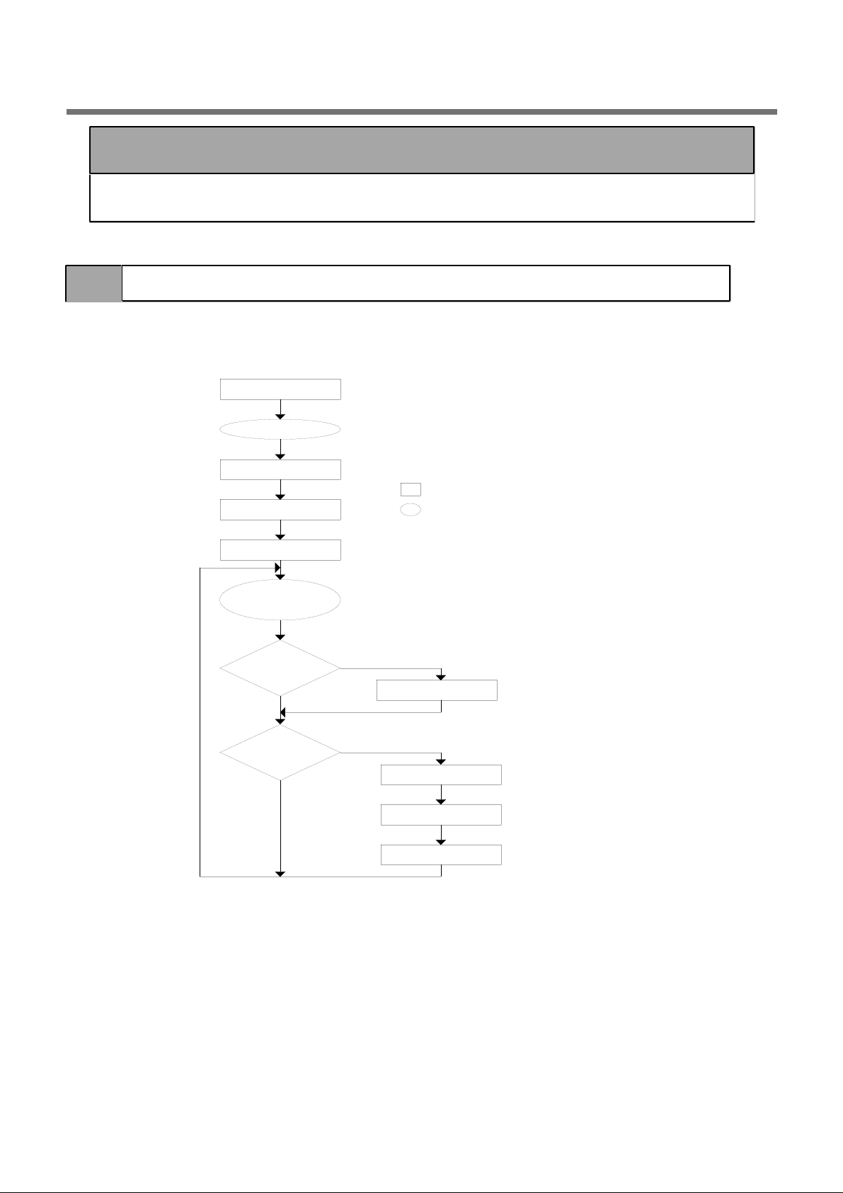
6.1 Basic Control Flow
Figure 6.1 shows the basic flow of control procedure. For details, refer to 6.2 and the following sections.
Reset
Initial state
Set external I/F
: Action made upon M65863FP
Set operation mode
: Status of M65863FP
Cancel muting
Decoding state(*1)
Change
operation
mode?
N
Change
external I/F?
N
Figure 6.1 Basic Flow of Control
*1 :M65863FP changes through plural
states according to the operation
mode and sync lock/presence of error
(See section 6.5 for detail).
Y
Set operation mode
Y
Mute
Set external I/F
Cancel muting
MITSUBISHI ELECTRIC CORPORATION 43

Some of external interfaces and operation mode can be changed even while decoding. When changing
external interface, however, mute the output by using the control register muteonoff or external terminal
_AMUTE. When changing the operation mode, on the other hand, M65863FP automatically mutes the
output.
Figure 6.2 shows the operation during resetting. At least xxx is required for the period of asserting _RST. If
_RST is negated, M65863FP executes the initialization routine to set default values in the on-chip registers.
The initialization routine takes 0.2msec.
Upon completion of the initialization routine, set the external interface and decoding mode by writing over
the values of the control registers.
Product Note M65863FP
April 1998 Dolby Digital Decoder
CRC error in the transmitted data is detected, M65863FP mutes the output.
6.2 Resetting and Initial State
BCLK
Initialization routine
Changing from default value
(external I/F, decoding mode)
_AMUTE
DOx
_RST
Figure 6.2 Resetting
MITSUBISHI ELECTRIC CORPORATION 44

Set the following items by means of the control registers. For the details of the addresses and set values of
the control registers, refer to section 4.4.
Settings which can be changed while M65863FP is running.
1) Selection of input port
Control register : inportsel
Option :
2) Selection of input bit length
Control register : inbitlen
Option : 16 bit, 18 bit, 20 bit, 24 bit
3) AC-3/PCM input mode in DIR I/F
Control register : dirdatamode
Option : Automatic judgment of AC-3/PCM, fixing to AC-3, fixing to PCM (w/mute), fixing
to PCM (w/o mute)
4) Decoding stream number in DIR I/F
Control register : istmums
Option : b'000 - b'111
5) Selection of input format in the case of DIR/ADC
Control register : dirform
Option : I2C, MSB first right-justified, LSB first right-justified
6) Selection of output mode
Control register : dspif
Option : DAC I/F, DSP I/F
7) Selection of output format
Control register : dacform
Option : I2C, MSB first right-justified, LSB first right-justified
8) Output bit length
Control register : outbitlen
Option : 16 bit, 18 bit, 20 bit, 24 bit
If you want to change the above settings during PCM output, mute the output by using the control register
muteonoff or external terminal _AMUTE.
Items which can be set only once immediately after resetting
1) Selection of LRCK/BCLK mode
Control register : dacclkmode
Option : Generation by M65863FP (master), use of input ALRCK, ACLK (slave)
2) Whether dual stream decoding or not
Control register : asmix
Option : Single stream decoding, dual stream decoding
3) Number of sync words required before sync-lock
Control register : synclock
Option : 1 to 7
4) Input mode in the case of DEMUX I/F
Control register : burstcont
Option : Input till buffer-full, input frame by frame
5) Selection of SYNCRST function in the case of DEMUX I/F
Control register : syncrsten
Option : No use of SYNCRST, SYNCRST mode A, SYNCRST mode B
Product Note M65863FP
April 1998 Dolby Digital Decoder
6.3 Setting of External Interface
MITSUBISHI ELECTRIC CORPORATION 45

M65863FP supports the following operation modes. Mode varies depending on the setting of control
register and the input stream. Operation mode can be changed even during PCM output by M65863FP.
When changing the mode, M65863FP automatically mutes the output to prevent abnormal sound.
1) Dolby Digital (AC-3) + Pro Logic decoding mode
This mode is achieved when the following 2 conditions are satisfied.
a) Control register dirdatamode is 00 and AC-3 input is affirmed or control register dirdatamode is
01.
b) Control register pdecmode is 01, or pdecmode is 10 and dsumode in the input AC-3 stream is
10.
2) Dolby Digital (AC-3) decoding mode
This mode is achieved when the following 2 conditions are satisfied.
a) Control register dirdatamode is 00 and AC-3 input is affirmed, or control register dirdatamode is
01.
b) Control register pdecmode is 00, or pdecmode is 10 and dsumode in the input AC-3 stream is
other than 10.
3) PCM + Pro Logic decoding mode (on/off switching of de-emphasis process enabled)
This mode is achieved when control register dirdatamode is 00 and PCM input is affirmed, or when
control register dirdatamode is either 10 or 11 and control register pdecmode is 01. Pro Logic
decoding mode can further be changed by means of control registers autobal and narwid. Deemphasis can be switched on/off by means of control register dempha and external terminal
DEMPHA.
4) PCM through mode (on/off switching of de-emphasis process enabled)
This mode is achieved when control register dirdatamode is 00 and PCM input is affirmed, or when
control register dirdatamode is either 10 or 11 and control register pdecmode is 00. De-emphasis can
be switched on/off by means of control register dempha and external terminal DEMPHA.
5) Noise output mode
This mode is achieved by setting a value 1 in any of control registers (lnoise, cnoise, rnoise, srnoise,
slnoise, swnoise).
Only the operation mode 1, 2 and 5 are supported in the case of DEMUX I/F. When control register
dirdatamode is 00, AC-3/PCM is automatically determined which is carried out by searching
IEC958sync preamble. M65863FP outputs the current status (AC-3 input/PCM input) through the
external terminal DIRSTAT. For details, refer to the description on control register dirdatamode in
section 4.4.
The following settings can be done in Dolby Digital (AC-3) decoding mode.
1) Number of output channels
Control register : outchmode
Option : 1ch to 5ch
2) Output during dual monaural mode
Control register : stereo
Option : Output of ch1 only, output of ch2 only, output of ch1 from Lch and ch2 from Rch,
output of ch1+ch2
3) Compression mode
Control register : compmod
Option : RF mode, LINE mode, custom A, custom B
4) Dynamic range compression scaling
Control register : hcompsc, lcompsc
Option : No compression (h'00) to Full compression (h'7f)
Product Note M65863FP
April 1998 Dolby Digital Decoder
6.4 Selection of Operation Mode
MITSUBISHI ELECTRIC CORPORATION 46

M65863FP takes the following states during Dolby Digital (AC-3) decoding. Current status can be checked
by means of the status register and external terminal. For detail, refer to 3. Input/output pins and 4.3 Status
register.
1) Out-of-sync status
State of being out of synchronization. Output is muted. In this state, when sync word is successfully
detected successively the number of times specified in the control register synclock, M65863FP
enters the normal decoding status.
2) Sync lock & muting status
A state in which output is muted because, although synchronization is established, an error was
detected in external direction (external terminal AMUTE, control register muteonoff) or in the stream.
M65863FP enters the normal decoding status when the external direction is canceled or the error in
the stream is removed. When detection of sync word fails twice successively, on the contrary,
M65863FP comes out of synchronization. When control register syncrsten is 01 or 10, assertion of
external terminal SYNCRST also results in the status of out of synchronization.
3) Normal decoding status
A state of decoding normally carried out with PCM being output. This state is achieved if
synchronization is locked and no error is detected in the data stream. When detection of sync word
fails 2 successively in this state, M65863FP comes out of synchronization. When control register
syncrsten is 01 or 10, assertion of external terminal SYNCRST also results in the status of out of
synchronization.
M65863FP autonomously changes through the above states except for the operations of the external
terminal SYNCRST.
Product Note M65863FP
April 1998 Dolby Digital Decoder
5) Dialog level adjustment
Control register : dialevel
Option : h'0000 (=0.0) to h'7fff (=1.0)
6.5 Decoding Status
Sync out
(Mute PCM output)
Synclock & Error (CRC)
Mute PCM output)
Normal decoding
(PCM output)
Figure 6.3 Decode status transition
MITSUBISHI ELECTRIC CORPORATION 47

When an error is detected in the data stream which is being input, or when directed by the control register
(muteonof)f and external (AMUTE), M65863FP mutes the output PCM. Specifically, muting operation is
carried out in the following cases.
1) CRC1/CRC2 error and encode error are detected during Dolby Digital (AC-3) decoding. Encode error
refers to a case when an abnormal value is detected in bitstream in spite of normal result of CRC
check.
2) sync preamble is detected when control register dirdatamode is 10 and PCM input is under way.
3) External terminal AMUTE is asserted.
4) Control register muteonoff is 1.
Mute ON/mute OFF operation when decoding Dolby Digital (AC-3) is carried out by using 256 samples by
means of the window function defined in Dolby Digital (AC-3).
Product Note M65863FP
April 1998 Dolby Digital Decoder
6.6 Muting Operation
0 dB
Audio
reproduction
- dB
Soft Mute ON Soft Mute OFF
256/fs 256/fs
Figure 6.4 Soft Mute Function
MITSUBISHI ELECTRIC CORPORATION 48

Dolby Digital (AC-3) decoding delay of M65863FP varies between the cases of DIR I/F input and DEMUX
I/F input.
<Decoding delay with DIR I/F>
Decoding delay is given by the following equation.
Decoding delay = 1 frame transmission time * 2/3 + 1 audio block period
For example, when sampling frequency is 48kHz and bit rate of stream data is 384 kbps (length of 1
frame is 768*16 bits), decoding delay becomes approx. 11ms because the two terms in the above
equation have the following values.
Transmission time of 1 frame: (768*16)/(48000*32)*2/3 = 5.3msec
1 audio block period : 256/48000 = 5.3msec
<Decoding delay with DEMUX I/F>
Decoding delay in the case of DEMUX I/F is different from the case of DIR I/F, because PCM output and
IEC958 output of AC-3 stream are synchronized. In the case of DEMUX I/F mode B, decoding delay is
different from the cases of other modes, because it is assumed that AC-3 stream has already been input
to the input buffer in this case.
When in mode A
Decoding delay = 1 frame transmission time + 1 audio block period
For example, when sampling frequency is 48kHz and AC-3 stream is continuously transmitted,
decoding delay becomes approx. 37msec.
Transmission time of 1 frame: 1536/48000 = 32msec
1 audio block period : 256/48000 = 5.3msec
When in mode B
Decoding delay = 1 audio block period
In the case of Dolby Digital (AC-3) decoding, M65863FP does not support surround/center delay. In
the case of Pro Logic decoding, surround delay is fixed at 15ms.
Product Note M65863FP
April 1998 Dolby Digital Decoder
6.7 Decoding Delay
MITSUBISHI ELECTRIC CORPORATION 49

One of Dual Mono,1/0,2/0,2/1,2/2,3/0,3/1,3/2 modes can be selected. The number of output channels
depends on the encoded data. Maximum channels are limited by the encoded data except for 1/0 encoded
data and Pro Logic encoded data.
In the case of 1/0 encoded data, 2/0 (monaural stereo) output mode can be selected. Pro Logic encoded
data is the same as the 3/1 mode. If a high number of channels beyond the input data channels is specified
for output in the output mode, the over-channels output data is '0'.
One of 4 output modes can be selected when the main audio services the Dual Mode.
Table 6.1 Output Channel Selection
Product Note M65863FP
April 1998 Dolby Digital Decoder
6.8 Output Mode
Output channel mode is controlled by the control register.
Encode Channel Mode Available Output Channel Form
1+1(Dual Mono) Ch1->L Ch1->R
Ch2->L Ch2->R
Ch1->L Ch2->R
1/0 1/0, 2/0 (monaural stereo)
2/0 1/0, 2/0
3/0 1/0, 2/0, 3/0
2/1 1/0, 2/0, 2/1, 2/2
3/1 1/0, 2/0, 3/0, 2/1, 2/2, 3/1, 3/2
2/2 1/0, 2/0, 2/1, 2/2
3/2 1/0, 2/0, 3/0, 2/1, 2/2, 3/1, 3/2
Pro Logic (2/0) 1/0, 2/0, 3/0, 2/1, 2/2, 3/1, 3/2
(Ch1+Ch2)->L (Ch1+Ch2)->R
MITSUBISHI ELECTRIC CORPORATION 50

ircuit and a frequency quadruplier (PLL) circuit by connecting an
oscillator element, resistor and capacitor on the outside. This enables it to generate the clock required for
the internal operation, though auto-oscillation by using low-frequency external clock.
Product Note M65863FP
April 1998 Dolby Digital Decoder
Chapter 7
Clock Oscillator
M65863FP allows it to form oscillation c
Internal Clock
M65863FP
PLL(x4)
PLL3
PLL2
PLL1
PCLK
Oscillation Buffer
Figure 7.1
PVCO
PLLGND
MITSUBISHI ELECTRIC CORPORATION 51

Oscillation circuit can be formed by connecting an oscillator element, a feedback resistor and load
capacitors to the PXCLK and PVCO terminals as shown bellow.
A frequency quadruplier circuit can be formed by connecting a loop filter to PLL3 terminal, a PLL stabilizer
resistor to PLL2 terminal and a current reference resistor to PLL1 terminal.
Product Note M65863FP
April 1998 Dolby Digital Decoder
7.1 Clock Oscillator
Cp
PCLK
M65863FP
PVCO
Rp
Cp
Symbol Value
Rp
Cp
1M
30pF
Figure 7.2 Configuration for Clock Oscillator
When extrnal clock is used
External clock can be directly to the PCLK terminal.
PCLK
M65863FP
External Clock
3.3V
Figure 7.3
7.2 Frequency Quadruplier Circuit
Symbol Value
Figure 7.4
MITSUBISHI ELECTRIC CORPORATION 52

BCLK
PLL3
PLL2
VDD3V
VDD5V
PLL1
PCLK
VDD3V
PLLVCC
2BCLK
2nd DSP assumes processes such as center/surround delay and crossover filter to be done. When
limited to AC-3 2ch output, output of M65863FP can be directly connected to DAC.
3) MCU I/F supports I2C I/F as well as the above (synchronized 4 line serial).
4) While M65863FP functions as clock master with respect to LRCK/BCLK of 2nd DSP and DAC, such
an application is possible as M65863FP functions as slave while ALRCK and ACLK from DIR/ADC
are supplied to 2nd DSP and DAC.
Product Note M65863FP
April 1998 Dolby Digital Decoder
Chapter 8
M65863FP Typical Configuration
An example of wiring for a system of Dolby Digital (AC-3) 6ch application is illustrated below.
MCU
DEMUX
AV6220A
Mute on/of
Analog audio
ADC
IEC958 input
_SS
MOSI
MISO
SCK
ADVLDD
ADATAP
ACLKP
ADREQN
Main/Sub chip I/F
VDD5V
ASOUT
CDATA
CCLK
RSYCREQ
SYNCRST
ADVLDS
ADATAS
ACLKS
VDD3V
GND
VDD5V
_ADREQ
_AMUTE
DOTX
DIRX
ALRCK1
ACLK1
ADATA
GND
GND
GND
NC/SO
HSDA/SI
HSCL/SCK
NC/_SS
TOP VIEW
(M65863FP)
MCU I/F selection
Status output
VDD5V
GND
MCUSEL
DIRSTAT
DECSTAT
Reset
_RST
VDD5V
CHIPMOD
MCLKSI[1]
MCLKSI[0]
GND
GND
GND
GND
PVCO
PLLGND
2LRCK
LRCK
DAC
PCM1710P
Master clock selection
SDO0
SDO1
BCKIN
LRCIN
DIN
SDO2
2nd DSP
DIR
M51581FP
MSTCK
LRCK
BCK
SDO
IEC958 output
ACLK2
ADATA
ALRCK2
VDD5V
DEMPH
De-emphasis on/off
GND
VDD5V
MCLKI
Master clock output
MCLKO
DOLR
HMCLKO
DOCW
DOSS
GND
SDI1
SDO0
Figure 8.1
<Complementary notes>
1) All or part of DEMUX, ADC and DIR can be connected to M65863FP as audio inputs.
2)
MITSUBISHI ELECTRIC CORPORATION 53

Product Note M65863FP
April 1998 Dolby Digital Decoder
Chapter 9
Electrical Characteristics
9.1 Absolute Maximum Ratings
Ta=25
Symbol Characteristics Value Unit
VDD5V Supply voltage (I/O) -0.3 to +6.5 V
VDD3V Supply voltage -0.3 to +4.5 V
PLLVCC Supply voltage (PLL) -0.3 to +4.5 V
VI Input voltage (I/O) GND-0.3≤VI≤VDD5V+0.3 V
Input voltage(PLL) GND-0.3≤VI≤PLLVCC+0.3 V
VO Output voltage(I/O) GND≤VO≤VDD5V V
Output voltage(PLL) GND≤VO≤PLLVCC V
Pb Power consumption 910 mW
Topr Operating temperature range -20 to +75 °C
Tstg Storage temperature -40 to +125 °C
9.2 Operating Conditions
Symbol Characteristics Condition for Measuvment min typ max
VDD5V Supply voltage(I/O) 4.5 5 5.5 V
VDD3V Supply voltage 3 3.3 3.6 V
PLLVCC Supply voltage(PLL) 3 3.3 3.6 V
VIH Input High voltage(I/O) 0.7XVDD5V - VDD5V V
VIL Input Low voltage(I/O) GND - 0.3XVDD5V V
fpclk Frequency at external clock - 10? -2 MHz
Value Unit
MITSUBISHI ELECTRIC CORPORATION 54

Product Note M65863FP
April 1998 Dolby Digital Decoder
9.3 DC Characteristics
Ta= -20 to 75, VDD5V=5V, VDD3V=3.3V, PLLVCC=3.3V
Value Unit
Symbol Characteristics Condition for Measuvment min typ max
IDD Supply Current fpclk=???MHz - - TBD mA
VOH Input High voltage (I/O) VDD5V=5V,IIOI<1µA 4.95 - - V
VOL Input Low voltage (I/O) VDD5V=5V,IIOI<1µA - - 0.05 V
IOH Output current (I/O), 2mA buffer VDD5V=4.5V,VOL=4.1V 2 - - mA
Output current (I/O), 4mA buffer 4 - - mA
IOL Output current (I/O), 2mA buffer VDD5V=4.5V,VOL=0.4V - - -2 mA
Output current (I/O), 4mA buffer - - -4 mA
IIH High input current (I/O) VDD5V=5.5V,VI=5.5V -10 - 10 µA
IIL Low input current (I/O) VDD5V=5.5V,VI=0V -10 - 10 µA
IOZH High off state output leak current (I/O) VDD5V=5.5V,VI=5.5V -10 - 10 µA
IOZL Low off state output leak current (I/O) VDD5V=5.5V,VI=0V -10 - 10 µA
MITSUBISHI ELECTRIC CORPORATION 55

Product Note M65863FP
April 1998 Dolby Digital Decoder
9.4 AC Characteristics
Characteristic of timing
<DIRADC IF>
tsu(ALRCK-ACLK) th(ACLK-ALRCK)
ACLKx
ALRCKx
ADATAx
tsu(ADATA-ACLK) th(ACLK-ADATA)
Symbol Characteristics min typ max Unit
tsu(ALRCK-ACLK) Setup time, ALRCK and ACLK 5 - - ns
th(ACLK-ALRCK) Hold time, ALRCK and ACLK 6 - - ns
tsu(ADATA-ACLK) Setup time, ADATA and ACLK 8 - - ns
th(ACLK-ADATA) Hold time, ADATA and ACLK 8 - - ns
<DEMUX IF>
ACLKS
th(ACLKS-ADVLDS)
tsu(ADVLDS-ACLKS)
_ADREQ
ADVLDS
ADATAS
tsu(ADATAS-ACLKS) tsu(ACLKS-ADATAS)
Symbol Characteristics min typ max Unit
tsu(ADVLDS-ACLKS) Setup time, ALRCK and ACLKS 5 - - ns
th(ACLKS-ADVLDS) Hold time, ALRCK and ACLKS 6 - - ns
tsu(ADATAS-ACLKS) Setup time, ADATA and ACLKS 8 - - ns
th(ACLKS-ADATAS) Hold time, ADATA and ACLKS 7 - - ns
MITSUBISHI ELECTRIC CORPORATION 56

Product Note M65863FP
April 1998 Dolby Digital Decoder
<DAC IF>
tdv(BCLK-LRCK)
BCLK
LRCK
DOxx
tdv(BCLK-DO)
Symbol Characteristics min typ max Unit
tdv(BCLK-LRCK) LRCK output delay - - 15 ns
tdv(BCLK-DO) DO output delay - - 25 ns
<DSP IF>
2BCLK
LRCK
2LRCK
DOxx
tdv(2BCLK-LRCK)
tdv(2BCLK-2LRCK)
tdv(2BCLK-DO)
Symbol Characteristics min typ max Unit
tdv(2BCLK-LRCK) LRCK output delay - - 15 ns
tdv(2BCLK-2LRCK) 2LRCK output delay - - 15 ns
tdv(2BCLK-DO) DO output delay - - 25 ns
MITSUBISHI ELECTRIC CORPORATION 57

Product Note M65863FP
April 1998 Dolby Digital Decoder
<Clocked serial MCU I/F>
EIAJ Package Code JEDEC Code Weight(g) Lead Material
QFP68-P-1014-0.65 ---
tsu(SS-SCK)
_SS
tdv(SCK-SO)
SCK
SO
SI
tsu(SI-SCK) th(SCK-SI)
Symbol Characteristics min typ max Unit
tsu(SS-SCK) Setup time, _SS and SCK 10 - - ns
th(SCK-SS) Setup time, _SS and SCK 10 - - ns
tdv(SCK-SO) SO output delay - - 15 ns
tdz(SS-SO) SO disable delay - - 10 ns
tsu(SI-SCK) Setup time, SI and SCK 10 - - ns
th(SCK-SI) Hold time, SI and SCK 10 - - ns
0.79
th(SCK-SS)
tdz(SS-SO)
Alloy 42
MITSUBISHI ELECTRIC CORPORATION 58

Product Note M65863FP
April 1998 Dolby Digital Decoder
Chapter 10
Package
MITSUBISHI ELECTRIC CORPORATION 59

Any parties intereted in the manufacture and sale of products incorporating Dolby Digital (AC-3)/Pro Logic
technologies will first require a license from Dolby Laboratories Licensing Corporation. Dolby Laboratories
has standard license agreements for this purpose, which have been signed by 200 organizations in over 30
countries.
Following is a list of procedures a customer must follow before they can manufacture and sell products
incorporating Dolby Digital (AC-3)/Pro Logic technologies.
1) The customer fills a confidential questionnaire to help Dolby Laboratories determine whether or not
the customer has the infrastructure, facilities and engineering expertise to develop, manufacture, and
sell a product meeting Dolby's specifications.
2) Once approved to proceed with development, the customer signs a product agreement with Dolby and
pays a predetermined initial fee. At this point Dolby provides the customer with complete technical
documentation and support.
3) The customer provides Dolby Laboratories with preliminary functional specification for review.
4) After specification approval the customer submits a product prototype for review.
5) Once the prototype is approved the countersigned copies of the agreement are returned to the
licensee(customer).
6) Licensee may sell the product.
Mitsubishi Electric Corporation reserves the right to make changes to its product(s) or information
contained herein without notice. No liability is assumed as a result of their use or application. No rights
under any patent accompanies the sale of any such product(s) or information.
Copyright (C)1998 MITSUBISHI ELECTRIC CORPORATION. All rights reserved.
Printed in Japan
April 1998
Product Note M65863FP
April 1998 Dolby Digital Decoder
Appendix A
Licensing Procedure Guidelines for
Dolby Digital (AC-3) / Pro Logic
MITSUBISHI ELECTRIC CORPORATION 60
 Loading...