


MITSUBISHI SEMICONDUCTOR (LSI)
M65762FP
QM-CODER
DESCRIPTION
The M65762FP is a compression and decompression LSI
conforming to the high efficiency encoding system (QM-Coder) in
the International Standard, the JBIG/JPEG (ITU-T Recommendations T.81 and T.82) for coding still images. It also conforms to the
International Standard (ITU-T Recommendation T.85) for facsimile.
The QM-Coder is an information dependent type which is capable
of completely restoring original image data, and is equipped with
the learning function to always optimize parameters according to
the statistical characteristics of images. The QM-Coder is therefore
superior in compression ratio compared with the existing binary
coding system (MH/MR/MMR) and can greatly improve the half
toning image (dithered half toning image) whose compression ratio
is especially poor.
FEATURES
• Completely conforms to the International Standard (ITU-T T.85)
for facsimile.
• Achieves encoding/decoding with the arithmetic coder (QMCoder) conforming to the recommendation of the International
Standard JBIG/JPEG.
• Is expected to conform to the International Standard for color
facsimile (T.Pallete-colour).
• High speed processing that puts into effect coding and decoding
at 40 million pixels per sec maximum.
• Is possible data-through processing without coding and decodin.
• Can select context
• Provides 10 pixel template model for minimum resolution
conforming to JBIG and can select 2-line or 3-line template
model.
• Built-in typical prediction function
• Capable of coding and decoding by using the typical prediction.
• Since use of the typical prediction does not require the
processing of the line (TP line) which is matched the previous
line's data, is capable of reducing data and processing time.
• Built-in adaptive template (AT) function
• Is capable of setting AT pixels before 127 pixels on the coding
line.
• Since It is possible to change the position of AT pixel in a
specified line, is capable of improving compression
characteristics even when image characteristic is changed in
the middle of the screen.
• Supporting multi-stripe
• When a page consists of more than one stripe, is capable of
repeating encoding/decoding process in stripes.
• Built-in load/store function of line memory Supporting multiple
planes and multi-stripe function
• Is capable of loading image data for reference line from
outside to line memory of the LSI and storing image data from
line memory to outside.
• Number of processing lines
• Is capable of issuing the start of processing (temporary stop
command) several times to encode/decode any lines more
than or equal to 65535 lines.
• Supporting 3-bus interface
• An 8-bit host bus corresponds to the MPU is available to load
and store of context table RAM.
• For input/output of binary image data, is capable of performing
32-bit or 16-bit parallel or serial input/output.
• For input/output of coding data, is capable of selecting 32-
bit/16-bit/8-bit bus to perform DMA transfer of coding data.
• Is capable of making scale-down for coding and scale-up for
decoding.
• Is capable of setting marker code for coding and detecting
marker code for decoding.
• Built-in RAM for 4096 bytes for line memory, built-in context table
RAM and built-in probability estimation table ROM of 113 status
• +5V single power supply
APPLICATION
• OA equipment including facsimile, copier and printer
• Digital and amusement equipment for the purpose of reducing
memory
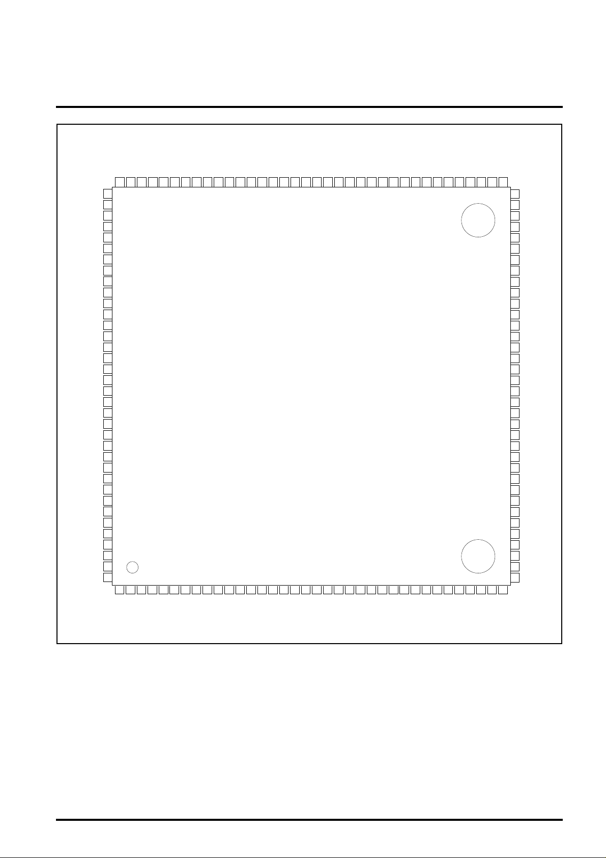
PIN CONFIGURATION (TOP VIEW)
MITSUBISHI SEMICONDUCTOR (LSI)
M65762FP
QM-CODER
CDAK
CDRD
CDWR
INTR
V
DD
GND
HD0
HD1
HD2
HD3
HD4
V
DD
GND
HD5
HD6
HD7
TEST0
TEST1
V
DD
GND
MCLK
V
DD
GND
RESET
HRD
HWR
HCS
VDD
GND
HA0
HA1
HA2
HA3
TOUT1
TOUT2
VDD
DD
CDRQ
V
CD31
106
105
CD30
104
GND
108
107
109
110
111
112
113
114
115
116
117
118
119
120
121
122
123
124
125
126
127
128
129
130
131
132
133
134
135
136
137
138
139
140
141
142
143
144
123456789
CD29
103
CD28
102
GND
101
100
DD
V
CD25
CD27
CD26
CD24
999897969594939291908988878685848382818079787776757473
101112131415161718
CD23
DD
V
GND
M65762FP
M65762FP
CD22
CD21
CD19
CD18
CD20
2021222324252627282930313233343536
19
GND
CD17
CD16
CD15
CD13
VDD
CD14
GND
VDD
CD12
CD11
CD10
CD9
CD8
GND
72
71
70
69
68
67
66
65
64
63
62
61
60
59
58
57
56
55
54
53
52
51
50
49
48
47
46
45
44
43
42
41
40
39
38
37
VDD
CD7
CD6
CD5
CD4
GND
DD
V
CD3
CD2
CD1
CD0
GND
DD
V
PXCKO
RVID
SVID
PXCK
PTIM
PRDY
GND
VDD
PDWR
PDRD
PDAK
PDRQ
GND
VDD
PD31
PD30
PD29
GND
VDD
PD28
PD27
PD26
25
PD
GND
PD0
PD1
PD2
PD3
PD4
PD5
GND
VDD
PD6
PD7
PD8
PD9
DD
GND
V
PD10
PD11
PD12
PD13
PD14
DD
PD15
PD16
GND
V
PD17
PD18
PD19
DD
GND
V
PD20
PD21
PD22
PD23
PD24
VDD
GND
Outline144P6Q-A
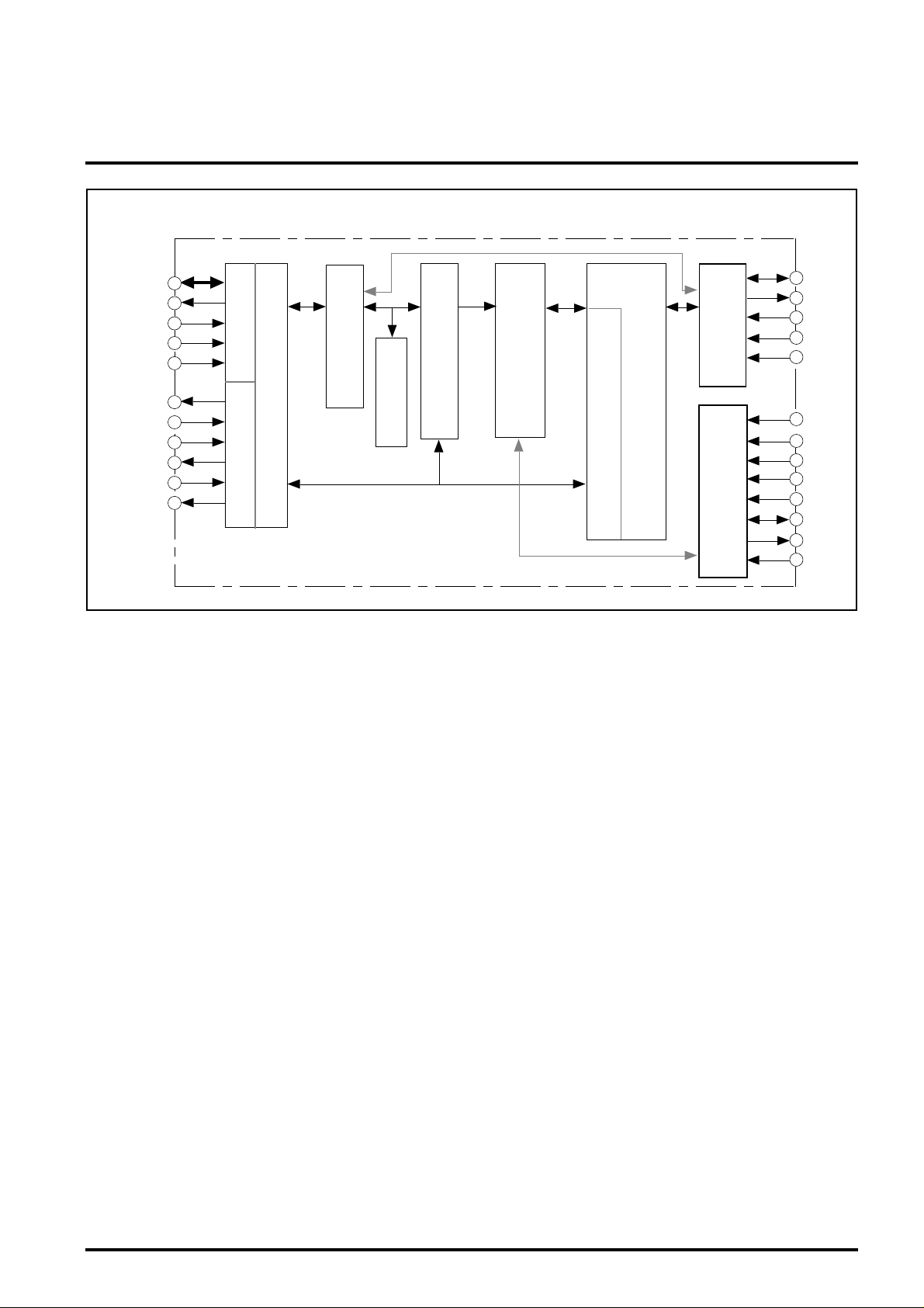
BLOCK DIAGRAM
MITSUBISHI SEMICONDUCTOR (LSI)
M65762FP
QM-CODER
PD0-31
PDRQ
PDAK*
PDRD*
PDWR*
PRDY*
PTIM*
PXCK*
PXCKO*
SVID*
RVID*
48
49
50
51
54
55
56
59
57
58
Parallel I/F
Image data I/F
Serial I/F
Line memory
Pixel data
Description on Block Functions
(1) Host bus I/F block
This bus is used to set command parameters and load the
status between the MPU and this block. It is 8-bit bus, This
block is also available to load and store of context table RAM
via the host bus.
(2) Code data I/F block
Bus for input/output of coding data. For the bus width, 32bits, 16-bits or 8-bits can be selected.
Image data can also be transferred (in through mode)
between the Image data I/F and this block via built-in line
memory. FIFO buffer for 16 bytes are provided in the code
data I/F block.
(3) Image data I/F block
The Image data I/F is used for input/output of binary image
data. The 32-/16-bit parallel I/F or serial I/F can be selected.
Selection of the serial I/F transfers data in units of 1 pixel in
synchronization with the line, using the handshake signal
(PRDY*, PTIM*).
Selection of parallel I/F uses an external DMA controller for
DMA transfer (in units of stripe).
The image data I/F provides a function for scale-down of
length and breadth by 1/2 in coding and a function for scaleup of length and breadth by twice in decoding.
Context generation
Typical prediction
108
109
110
111
132
135
134
133
112
129
Context table RAM
Encoding/decoding
Probability Estimation Table ROM
(Asterisk "*" indicates negative logic.)
Code data I/F
Host bus I/F
(5) Typical prediction block
In the typical prediction mode,comparesthe encoding/
decoding process line agree with the immediately preceding
line and generates pseudo-pixel (SLNTP).
(6) Context generator
By using the 10 pixel template of 2-lines or 3-lines.(including
AT pixel) the standard context minimum of JBIG is generated
with the resolution.
(7) Context table RAM block
Corresponds to the 10-bit standard context. This block can
initialize, load and store the context table RAM.
(8) Coding/decoding block
This block performs arithmetic coding and decoding.
It contains a ROM which contains a table capable of
estimating 113 states and is capable of byte stuffing function
('OO' byte insertion/rejection) and is capable of end marker
code control (Marker insertion/detection).
CD0-31
CDRQ
CDAK*
CDRD*
CDWR*
RESET*
HCS*
HA0-3
HWR*
HRD*
HD0-7
INTR
MCLK
(4) Line memory block
4K-byte memory. This block can be set to a maximum of
8192 pixels/line for 3-line template and can be set to a
maximum of 10240 pixels/line for 2-line template. A line is
used for input/output processing of image data to/from
outside and the other lines (2 or 3 lines) are used for
encoding/decoding processing. These two processes can be
independently carried out in synchronization with each line.
The contents of line memory can be loaded or stored via
the image data I/F or coding data I/F.
DESCRIPTION PIN
MITSUBISHI SEMICONDUCTOR (LSI)
M65762FP
QM-CODER
Pin No.
1
2
3
4
5
6
7
8
9
10
11
12
13
14
15
16
17
18
19
20
21
22
23
24
25
26
27
28
29
30
31
32
33
34
35
36
37
38
39
40
41
42
43
44
45
46
47
48
49
50
I/O Pin name
Power supply
I/O
I/O
I/O
I/O
I/O
Power supply
Power supply
I/O
I/O
I/O
I/O
I/O
Power supply
Power supply
I/O
I/O
I/O
I/O
I/O
Power supply
Power supply
I/O
I/O
I/O
I/O
I/O
Power supply
Power supply
I/O
I/O
I/O
I/O
I/O
Power supply
Power supply
I/O
I/O
I/O
I/O
Power supply
Power supply
I/O
I/O
I/O
Power supply
Power supply
O
I
I
GND
PD0
PD1
PD2
PD3
PD4
VDD
GND
PD5
PD6
PD7
PD8
PD9
VDD
GND
PD10
PD11
PD12
PD13
PD14
VDD
GND
PD15
PD16
PD17
PD18
PD19
VDD
GND
PD20
PD21
PD22
PD23
PD24
VDD
GND
PD25
PD26
PD27
PD28
VDD
GND
PD29
PD30
PD31
VDD
GND
PDRQ
PDAK
PDRD
Pin No.
51
52
53
54
55
56
57
58
59
60
61
62
63
64
65
66
67
68
69
70
71
72
73
74
75
76
77
78
79
80
81
82
83
84
85
86
87
88
89
90
91
92
93
94
95
96
97
98
99
100
I/O
I
Power supply
Power supply
O
I
I
I
O
O
Power supply
Power supply
I/O
I/O
I/O
I/O
Power supply
Power supply
I/O
I/O
I/O
I/O
Power supply
Power supply
I/O
I/O
I/O
I/O
I/O
Power supply
Power supply
I/O
I/O
I/O
I/O
I/O
Power supply
Power supply
I/O
I/O
I/O
I/O
I/O
Power supply
Power supply
I/O
I/O
I/O
I/O
I/O
Power supply
Pin name Pin name
PDWR
VDD
GND
PRDY
PTIM
PXCK
SVID
RVID
PXCKO
VDD
GND
CD0
CD1
CD2
CD3
VDD
GND
CD4
CD5
CD6
CD7
VDD
GND
CD8
CD9
CD10
CD11
CD12
VDD
GND
CD13
CD14
CD15
CD16
CD17
VDD
GND
CD18
CD19
CD20
CD21
CD22
VDD
GND
Pin No.
101
102
103
104
105
106
107
108
109
110
111
112
113
114
115
116
117
118
119
120
121
122
123
124
125
126
127
128
129
130
131
132
133
134
135
136
137
138
139
140
141
142
143
144
I/O
Power supply
I/O
I/O
I/O
I/O
Power supply
Power supply
O
I
I
I
O
Power supply
Power supply
I/O
I/O
I/O
I/O
I/O
Power supply
Power supply
I/O
I/O
I/O
I
I
Power supply
Power supply
I
Power supply
Power supply
I
I
I
I
Power supply
Power supply
I
I
I
I
O
O
Power supply
GND
CD28
CD29
CD30
CD31
VDD
GND
CDRQ
CDAK
CDRD
CDWR
INTR
VDD
GND
HD0
HD1
HD2
HD3
HD4
VDD
GND
HD5
HD6
HD7
TEST0
TEST1
VDD
GND
MCLK
VDD
GND
RESET
HRD
HWR
HCS
VDD
GND
HA0
HA1
HA2
HA3
TOUT1
TOUT2
VDD
CD23
CD24
CD25
CD26
CD27
VDD
(Notes) • Directly connect the input pin having pull-up (see Section 3.3.2 "Pin Function") to Vcc when the pin is not used.
• Directly connect the input pin having pull-down (see Section 3.3.2 "Pin Function" to GND when the pin is not used.
• Connect test input pin TEST 0/1 to GND.
• Leave test output pin TOUT 1/2 open.
MITSUBISHI SEMICONDUCTOR (LSI)
M65762FP
QM-CODER
Descriptionon Pin Functions
I/F Pin name I/O BUF Function
Host bus I/F
Code data I/F
Parallel
RESET*
HCS*
HA0-3
HWR*
HRD*
HD0-7
INTR
CD0-31
CDRQ
CDAK*
CDRD*
CDWR
PD0-31
PDRQ
PDAK*
PDRD*
PDWR*
O
I/O
O
I/O
O
I
I
I
I
I
I
UR8
I
US
I
US
I
US
UR8
I
US
I
US
I
US
H/W reset signal
S
Chip select signal
Address select signal of internal register
Write strobe signal
S
Read strobe signal
S
Input/output data bus signal
R8
Interrupt request signal
4
Coding data input/output bus signal
(CD0-15 is used in 16-bit bus and CD0-7 is used in 8-bit bus.)
DMA request signal for coding data (image data)
4
DMA acknowledge signal for coding data (image data)
Read strobe signal for coding data (image data)
Write strobe signal for coding data (image data)
Parallel image data input/output bus (PD0-15 is used in 16-bit bus.)
DMA request signal for image data
4
DMA acknowledge signal for image data
Read strobe signal for image data
Strobe signal for image data
(Asterisk "*" in signal name indicates negative logic.)
PRDY*
PTIM*
Image data I/F
PXCK*
PXCKO*
Serial
SVID*
RVID*
MCLK
TEST0, 1
Others
VDD
GND
• Input buffer for the input pins ("I" and "IO") are set at the TTL level and the options are as follows.
• Numbers (4, 8) in the BUF column for the output pins ('O' and 'IO') indicate Io (= 4 or 8 mA).
O
I
US
I
US
O
I
U
O
I
I
DS
–
–
(U: Having pull-up resistance, D: Having pull-down resistance, S: Schmitt trigger, R: Through rate control)
1-line input/output start ready signal for image data
4
1-line transfer sector signal for image data
Transfer clock signal for image data
Transfer clock signal for image data (LSI internal loopback output signal of PXCK*)
4
Image data input signal
Image data output signal
4
Master clock input signal
Test input signal 0/1 (Should be connected to GND when used normally.)
Power supply (+5V)
–
Ground
–
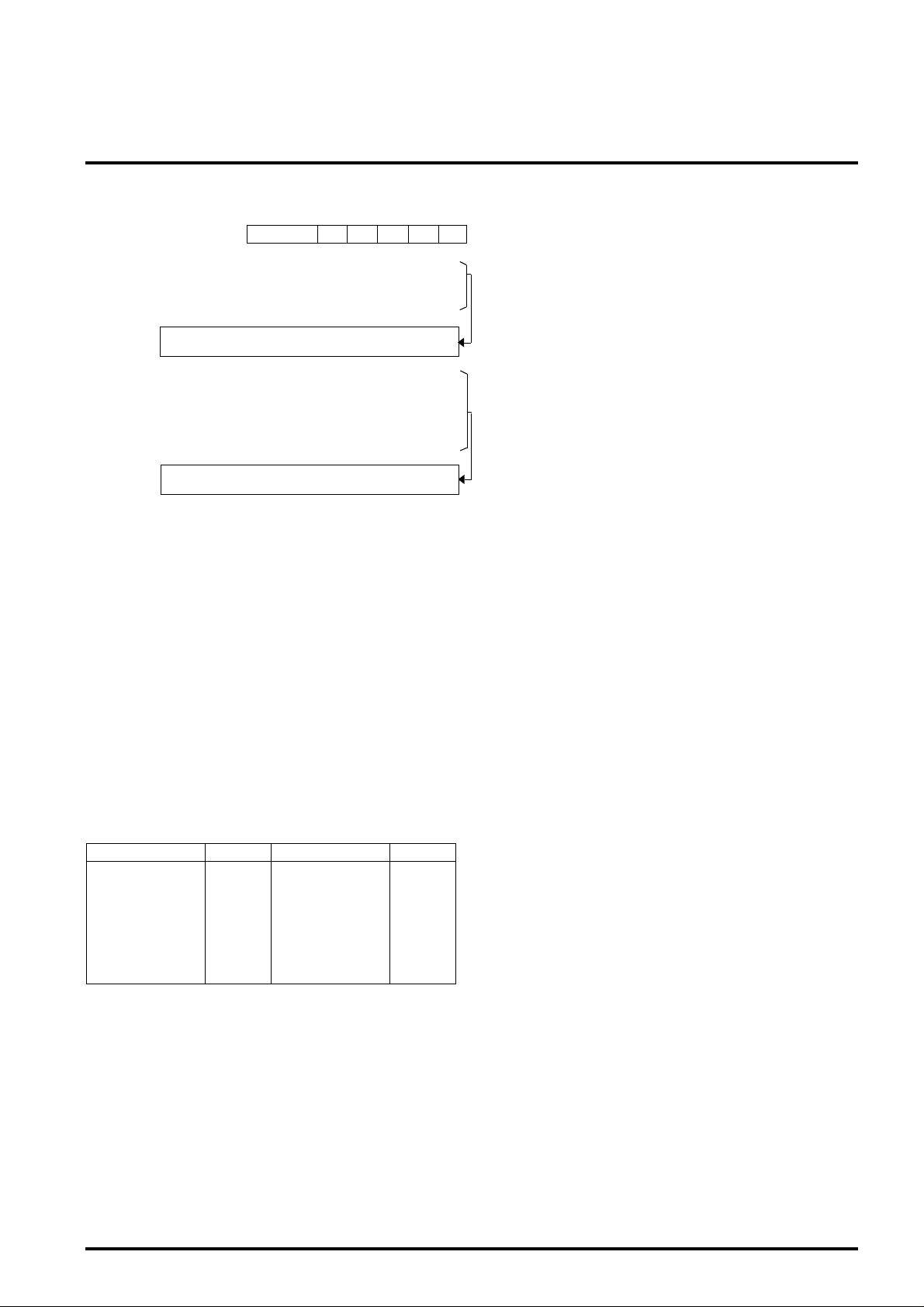
Specificatio ns
(1) Package
Plastic QFP 144 pins (20 mm*20 mm)
(2) Power consumption
5V 120mA (600mW)
(3) Maximum clock frequency
40MHz
MITSUBISHI SEMICONDUCTOR (LSI)
M65762FP
QM-CODER
Specifications of Coding Functions
(1) Coding algorithm
• QM-Coder (JBIG standard arithmetic coding system)
(2) Context
a) Template model
• 2- or 3-line of 10 pixel template (See Figure 1.)
(Conforming to the template for JBIG minimum resolution)
(Note) The coding efficiency of the 3-line template is better
than that of 2-line template by several %.
b) Adaptive template (AT)
• It is possible to move up to 127 pixels on the coding line.
(AT position is indicated by MPU.)
(Note) AT is available to improve the coding efficiency for
• Even in the middle of coding/decoding , the position of AT
(3) Typical Prediction
dither image.
line can be changed for a line (ATmove)
(Note) When the position the AT pixel of is changed, the
template model cannot be changed concurrently.
X X
X
X X X
X X
X X X X
X
X X
Figure 1 Template (X, A)
A
A X X
X X
(Upper: 3 lines, Lower: 2 lines)
MAX127
X
MAX127
Figure 2. Adaptive Template (A)
X A
?
A
?
X X X
X X X X
X X
X X X X
X X
?
?
• Agreement with the typical prediction of the minimum
resolution of JBIG.
The psedo-pixel (SLNTP) is generated by the symbol LNTP
which shows whether the coding/decoding process lines
agree with the immediately preceding line. If they agree, the
pesudo-pixel only is coded. This makes it possible to shorten
the time of process and rejection of the code data.
SLNTPy = !(LNTPy LNTPy-1) (where: y indicates a line
No., y = 1 indicates that lines do not match each other, and
initial value LNTP for head line is given with y - 1 = 1)
(4) Coding data format
• The stripe data entity (SDE = stripe coded data with byte
stuffing (PSCD) + end marker (SDNORM/SDRST)).
Performs coding and decoding of one stripe (See Attached
Figure A.1.)
In the case of multi-striped (multi-stripes), can be supported
by activation for each stripe.
(5) Marker code
• Supports the SDE end marker (During coding, the marker
code previously set in the register is outputted. During
decoding, the marker code byte detected by requesting on
interrupt to MPU when the maker is detected is read out of
the register.)
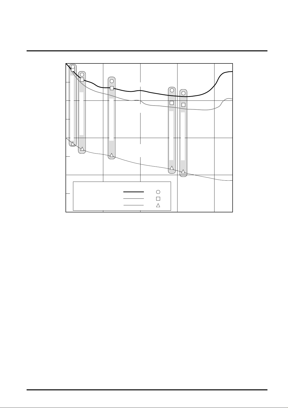
(6) Estimation of coding/decoding speed
Figure 3 compares the estimation of coding/decoding speed
between the M65762FP and the existing product type
(M65760/1FP). Polygonal lines in the diagram are processing
speeds of images theoretically generated assuming the
unmatched estimation ratio as a parameter. In addition, ,
indicate processing speeds of real image (without TP
function).
As shown in this diagram, the M65762FP has been largely
improved in the processing speed compared with existing
product types. If the compression ratio is reduced, the
reduction ratio of processing speed is moderated.
When a theoretical image is used to compare processing
speeds in the worst case, the processing speed of existing
product type is about 9.4M pixels/sec (1/compression ratio is
about 1), while the processing speed of the M65762FP is
about 27.5M pixels/sec (1/compression ratio 0.9) for coding
and is about 31.2M pixels/sec (1/compression ratio 0.75) for
decoding.
+
40
g
MITSUBISHI SEMICONDUCTOR (LSI)
M65762FP
QM-CODER
35
30
25
Baud rate and dither images
Average of test charts 1 to 8 of former CCITT
20
15
Processing speed (M pixels/sec.)
10
(Legend)
5
Decoding of M65762FP
Coding of M65762FP
Coding/decoding of existing
0
product type
0.25
0
Decoding of M65762FP
Coding of
M65762FP
Cafeteria and dither images
Coding/decoding of
existing product
type (M65760/1FP)
Theoretical
ima
e
0.5
Actual
image
Baud rate, error diffusion image
Cafeteria, error diffusion image
0.75
1.0
1.2
1/compression ratio
Figure 3 Estimated Processing Speed
Register Configuration
g
1. List of Registers
Table 1 List of Registers
MITSUBISHI SEMICONDUCTOR (LSI)
M65762FP
QM-CODER
Address
1 Parameter setting W/R
2 Command W
2 Status R
Register name
0 System setting W/R
R/W
Content
- LSI H/W reset
- Selects bit width of code data bus (32 bits/16 bits/8 bits).
- Selects coding (image) data byte swap on code data bus.
- Selects coding (image) data bit swap on code data bus.
- Selects image data bit swap on image data bus.
- Selects image data I/F (parallel I/F and serial I/F).
- Selects bit width of image data bus (32 bits/16 bits).
- Template selection (3-line template/2-line template).
- Sets up the AT pixel position (127 max).
(When set to 0, selects non-AT (default position).)
- Context table RAM initializing processing command
- Start/stop command
(Coding/decoding, image data through, load/store of the line memory)
- Start/stop command of load/store of context table RAM
- Selects temporary stop/termination end mode.
- Processing status (in process/end of process)
- Ready for reading/writing coding (image) data on code data bus
- Detects marker code (SDNORM, SDRST, ABORT, etc.).
- Interrupt request status
- SC counter overflow error
- Processing mode (temporary stop/end of termination)
Interrupt enable
3
setting
Setting number of
4, 5
pixels
Setting number of
6, 7
lines
Number of
8, 9
processin
Load/store bufferA
Operation mode
B
setting
C
Marker code setting
C Marker code reading R
Scale-up/
D
scale-down setting
lines
W/R
W/R
W/R
R
W/R
W/R
W
W/R
- Interrupt enable setting corresponding to each bit position of status register
- Indicates pause/restart with marker code detected (at time of decoding)
- Sets the number of pixels per line.
(a maximum of 10240 pixels with 2-line template selected)
- Sets the number of lines to be coded/decoded (1 line or more, a maximum of 65535
lines)
- Number of setting the coded/decoded lines (a maximum of 65535 lines)
- Buffer register that loads/stores context table RAM data from the MPU.
(RAM address is automatically incremented each time data is written/read.)
- Sets the operation mode.
(Coding/decoding, image data through, and load/store of line memory)
- Selects read-through of head coding data in decoding (0 ~ 3 bytes).
- Selects the typical prediction function.
- Selects prohibition of line memory initialization.
- Sets the terminal marker code in encoding (SDNORM/SDRST)
- Reads a marker code in decoding.
(SDNORM, SDRST, ABORT, others)
- Scale down in coding (1/2 scale-down of horizontal and vertical, horizontal OR
processing)
- Scale-up at time of decoding (scale-up of horizontal and vertical by twice)
2. Description on Register
(
(1) System setting register (W/R)
(Address: 0)
SYS_REG: PB PI BX BS DS CB HR
d0 (HR): H/W reset (0: Active status, 1: Reset status)
d1-2 (CB): Selects the bit width of code data bus (d2 = 0, d1 = 0:
d7(MSB)
To reset H/W, set this bit to 1 then to 0. The entire LSI
including register group and line memory is initialized
by writing in this reset. However, context table RAM is
not initialized.
8-bit bus (CD0-7), d2 = 0, d1 = 1: 16-bit bus (CD0-15),
d2 = 1, d1 = 0: 32-bit bus (CD0-31))
(Note1)Prohibition of setting for d2 = 1, d1 = 1
(Note2)For encoding in 16-/32-bit bus, the last
encoding data is output followed by bit byte of
'00' (3 bytes maximum) for word alignment of
encoding data at the end.
d0(LSB)
MITSUBISHI SEMICONDUCTOR (LSI)
M65762FP
QM-CODER
d4 (BS): Selection of data bit swap of code data bus (0: MSB
first, 1: LSB first) See Table 2.
d5 (BX): Selection of data byte swap of code data bus (0: low
order byte first, 1: high order byte first) See Table 2.
(Note) BX is effective only when the host bus selects
16-bit/32-bit bus.
d6 (PI): Selection of image data input/output I/F (0: serial I/F, 1:
parallel IF)
d7 (PB): Selection of bit width of image data bus (0: 32-bit bus
(PD0-31), 1: 16-bit bus (PD0-15) See Table 3.
Note) PB and DS are effective only when PI = 1.
d3 (DS): Selects data bit swap of image data bus (0: MSB first, 1:
LSB first) See Table 3.
Table 2 Line up of Coded Data/Image Data in Code Data Bus
Bus width (CB)
d2 d1 d5 d4
01
(32-bits)
01
(16-bits)
00
(8-bits)
Note) b0 is image data, given in time series, on the left side of the first encoding data/screen. b31 is image data, given in time series, on the right side of the last encoding data/screen.
Swap (BX, BS)
0
0
0
1
1
0
1
1
0
0
0
1
1
0
1
1
–
0
–
1
CD31 • • CD24 CD23 • • CD16 CD15 • • CD8 CD7 • • CD0
b24 • • b31
b31 • • b24
b0 • • b7
b7 • • b0
–
–
–
–
–
–
Order of data in code data bus (CD)
b16 • • b23
b23 • • b16
b8 • • b15
b15 • • b8
–
–
–
–
–
–
b8 • • b15
b15 • • b8
b16 • • b23
b23 • • b16
b8 • • b15
b15 • • b8
b0 • • b7
b7 • • b0
–
–
b0 • • b7
b7 • • b0
b24 • • b31
b31 • • b24
b0 • • b7
b7 • • b0
b8 • • b15
b15 • • b8
b0 • • b7
b7 • • b0
Table 3 Order of Image Data on Image Data Parallel Bus
Bit width
PB=0
PB=1
p0 is image data on the left side of the screen. p31 is image data on the right side of the screen.
(2) Parameter setting register (W/R)
Swap
DS=0
DS=1
DS=0
DS=1
PD31 • • • • PD16
p0 • • • • p15
p31 • • • • p16
–
PD15 • • • • PD0
p16 • • • • p31
p15 • • • • p0
p0 • • • • p15
p15 • • • • p0
(Address: 1)
PARA_REG :
d7 d4
d0-4 (AT<0>-AT<4>): Low order 5-bits of AT pixel position (See
Figure 2.)
d5 (TM): Selection of template (0: 3-line template, 1:
2-line template)
d6-7 (AT<5>-AT<6>): High-order 2-bits of AT pixel position
(6th/7th bit)
(Example) 3-line template, AT = 4
2-line template, AT = 48
(Note) AT pixel position is set (0 to 127) with AT <6:0>.
At the default position (AT pixel is not used), set AT = 0.
The 2-line template, prohibits AT = 1 to 4 from being set. The 3line template prohibits AT = 1 to 2 from being set.
d5d6
AT TM AT
d7 d4
0 0 0 0 0 1 0 0
0 1 1 1 0 0 0 0
d0
d0

MITSUBISHI SEMICONDUCTOR (LSI)
r
r
M65762FP
QM-CODER
(3) Command Register (W)
(Address: 2)
CMD_REG:
d0 (IC) :Context table RAM initialization start command (1: Start
initialization)
Setting this bit to 1 starts to initialize context table RAM.
When the initialization is completed automatically returns
this bit to 0.
d1 (JC) :Processing (coding/decoding/through) start/end
command (1: Start of processing, 0: End of processing)
Settin g t hi s bit to 1 start s proc es s in g(coding/decoding ,
imag e data throu gh and lead/s toreof lin e memory).
Before the issuance of this command, concrete
operation mode must be set in the operation mode setup
register.
When the processing for the number of setup lines ends
with the end of termination selected this bit automatically
returns to 0.
(Note)When this JC bit is set to 0 during the coding
d2 (RC) :Load/store start/end command of context table RAM (1:
Start of load/store, 0: End of load/store)
Setting this bit to 1 can load context data into context
table RAM from outside via a buffer register or can store
context data in outside. (See the section for buffer
register.)
When load/store processing is completed, this bit must
be set to 0.
d3 (JP) :Temporary stop mode of processing(coding/
decoding/through)/termination end mode selection
(1: Selection of temporary stop, 0: Selection of
terminationend) Issuance of processing start command
d1 (JC) with this JP bit set to 1 temporaril ystops
performing the process operation at the completion of
processing for the number of setup lines. After that,
reissuance of processing start command d1 (JC)
restarts processing. (See Section 4.(3).)
(4) Status register (R)
(Address: 2)
STAT_REG :
d0 (JS) :Processing (initialization/coding/decoding/through)
status (0: Processing in progress (temporary stop or
initial), 1: Completion of processing)
This JS bit is set to 1 in the following cases: when the
initialization is complete with the RAM initialization
command issued (IC = 1), when all coding data is read
completely at time of coding with the start command of
termination end processing issued (JC=1, JP=0), and
when all image data is read completely at time of image
data through and at time of decoding. When the
temporary stop processing start command is issued (JC
= 1, JP = 1), this JS bit remains to be 0, even if the
process for the number of setup lines ends. (However,
an interruption occurs at time of temporary stop.)
d7 d0
0 JP RC JC IC
process (is in progress,) and input of image data
is stopped, the coding is stopped (flashed) even if
the set lines are not filled. When this bit is set to 0
auring decoding process, and input of encoding
data ceases, processing for the number of setup
lines is carried out assuming coding data "00" to
have been input. In the case of multi-stripe
coding, however, process must not be stopped by
setting this bit to 0 except for the final stripe.
d7
d5
0 PS SC IS MS DS JS
d3
d0
When this bit is set to 1, data can be read/written on the
d2 (MS) :Detects marker code at time of decoding (0: Not
d3 (IS) :Status of interrupt request (INTR pin) (0: Not requested,
d4 (SC) :SC count-over error at time of coding (0: Normal, 1:
d5 (PS) :Processing (temporary stop/termination end) mode (1:
(5) Interrupt enable register (W/R)
(Address: 3)
d0 (JE) :Processing (initialization/coding/decoding/through)
d1 (DE) :Coding data (image data) read/write ready interrupt (0:
d2 (ME) :Marker code detection interrupt at time of decoding (0:
d3 (SE) :SC count-over error interrupt at time of coding (0:
d7 (MP) :Indication of pause at time of marker code detection (0:
code data bus. (This bit is equivalent to the CDRQ pin.)
detected, 1: Detected)
This bit is set to 1 when some marker code is detected at
time of decoding.
1: Requested)
Occurrence of SC counter overflow)
(Note)The SC counter is a counter for consecutive "FF"
data bytes generated in the coding process.
Though coding process continues if the SC
counter overflows, normal coding data is not
output (encoding error).
Temporary stop processing mode, 0: Termination end
processing mode)
This PS bit corresponds to the selection of process
temporary stop/termination end of the d3 (JP) bit of
command register.
d7
IENB_REG:
Temporary stop/termination end interrupt (0: Interrupt
mask, 1: Interrupt enable)
Interrupt mask, 1: Interrupt enable)
Interrupt mask, 1: Interrupt enable)
Interrupt mask, 1: Interrupt enable)
(Note)Bits d0 to d3 are interrupt enable of bits d0 to d2
Indication of continuation/restart, 1: Indication of
temporary pause)
If this MP bit is in advance set to 1 in decoding, the
decoding temporarily pauses at the time of marker code
detected.
(When the ME bit is set to 1, an interruption occurs when
marker code is detected.)
When decoding process is not completed at time of
temporary pause of marker detection, the register fo
setting the number of lines can be respecified (See Item
(7).) Afterwards, setting this MP bit to 0 restarts the
decoding process (the decoding process is carried out
for the number of set lines).
MP 0 SE ME DE JE
and d4 corresponding to the status register.
When one of the status bits set to interrupt enable
is set to 1, the interrupt request signal (INTR) is
asserted (for d0 (JE), an interrupt occurs even at
the time of temporary stop).
When the status is set to 0 by H/W reset etc., o
when interrupt factor is eliminated by interruption
masking, INTR is negated. The status register is
not cleared by occurrence of interruption or by
R/W of interruption enable register.
d3
d0
d1 (DS) :Ready for reading/writing coding data (image data case
of the through mode) on the code data bus (1: Ready, 0:
Read/write disabled)

MITSUBISHI SEMICONDUCTOR (LSI)
M65762FP
QM-CODER
(6) Register for setting the number of pixels (W/R)
d7
(Address: 4)
(Address: 5)
d0-7 (PEL_L) :Sets the number of pixels in a line. (Low byte)
d0-5 (PEL_H) :Sets the number of pixels in a line. (Upper byte)
(7) Register for setting the number of lines (W/R)
(Address: 6)
(Address: 7)
d0-7 (LSET_L) :Sets the number of lines to be processed. (Low
d0-7 (LSET_H) :Sets the number of lines to be processed. (High
Figure 4. Address Assignment of Context Table RAM
(Number for address bit (LSB: 0, MSB: 9), MSB: 9 for AT pixel)
PEL_REG_L:
PEL_REG_H:
A maximum of 8192 pixels can be set at the 3-line
template. A maximum of 10240 pixels can be set
at the 2-line template.
Set the number of pixels to be actually coded
(decoded) at time of scale-up (scale-down).
When the image data bus is 16-bits (32-bits) with
the parallel I/F selected, set the number of pixels to
multiples of 16 (multiples of 32).
With the serial I/F selected, set the number of
pixels to multiples of 8.
LSET_REG_L:
LSET_REG_H:
order byte) (1 to 65535: 0 line is not allowed.)
order byte)
At time of scale-down (scale-up), set the number of
lines to be actually coded (decoded).
Set the number of lines (number of relative lines)
ranging from the processing start command to be
issued next to the temporary stop/termination end
just after. This register must be set to a specific
value before the issuance of the process start
command.
As far as the following conditions are satisfied, this
register can be rewritten in the course of
processing.
•When the maximum value (65535) is set before
issuance of the processing start command, an
arbitrary value can be set once in the course of
processing.
•When a value except for the maximum value
(65535) is set before issuance of the processing
start command, and the value requires to be
respecified in the course, respecify the maximum
value (65535) once and then respecify a desired
value.
876
54329
01
?
3-line template
PEL_L
0
d7 d0
d7 d0
2-line template
PEL_H
d5
LSET_L
LSET_H
5432
89
01
?67
(8) Processing line count register (R)
d0
(Address: 8)
(Address: 9)
d0-7 (LINE_L) :Read out the number of lines actually processed
d0-7 (LINE_H) :Read out the number of lines actually processed
(9) Buffer register (W/R)
(Address: A)
d0-7 (DWR) :Data for loading/storing context table RAM
LIN_REG_L:
LIN_REG_H:
(low byte) (0 to 65535)
(upper byte)
The number of processed lines ≥ number of set
lines, coding/decoding/through processing stop
temporary/end of processing.
(Note)The number of lines in this process is cleared
to 0 with the processing start command issued.
DWR_BUF: DWR
This register is a buffer for loading data into t h e
context table RAM via the host bus or for storing
data outside. After issuance of load/store start
command of the context table RAM (command
register d3 = 1), this register is available to start
loading or storing data. Prediction value (MPS) and
prediction unmatched probability (LSZ) can be
stored in context table RAM for a unit of 1024
contexts in total. Figure 4 and Table 4 provide the
address assignment of context table RAM and the
data bit array.
Since context table RAM is 2-byte data, access is
gained alternately in order from low byte to upper
byte. Each time two-byte access is gained, the
RAM address is automatically incremented
(sequential access from address 0).
(Note1)Data is not allowed to be loaded and stored
(Note2)Only 133 types specified by the JBIG
d7
LINE_L
LINE_H
d7
at a time. Random access to RAM is not
allowed.
international standard (See attached Figure
A.2) are allowed to be specified for the LSZ
value.
(For example, load '5a1d' for initialization.)
Table 4. Data Bit Array of Context Table RAM
High order byte Low order byte
d14 • • • • • d8
d15
MPS
L14 • • • • • L8
MPS :Prediction value MPS (0/1)
L14-0 :Low 15-bits of prediction unmatched probability LSZ
('0001' to '5b12')
d7 • • • • • d0
L7 • • • • • L0
d0
d0

MITSUBISHI SEMICONDUCTOR (LSI)
M65762FP
QM-CODER
(10) Operation mode setting register (W/R)
(Address: B)
MOD_REG:
This register is used to set the LSI operation mode and requires to
be set before issuance of the processing start command
(command register d1 (JC) = 1).
d0-1 (MOD) :Operation mode setting (d1 = 0, d0 = 0: Coding, d1 =
1, d0 = 0: Image data through (image data I/F Code
data I/F) load/store, d1 = 0, d0 = 1: Decoding, d1 = 1,
d0 = 1: Image data through (code data I/F Image
data I/F) load/store)
d2- 3 (LIO) :Load/store selection of image data of line memory
(d2 = selection of load, d3 = selection of store)
In the case of multi-stripe, this LIO bit is set according
to the following table, to load image data for
reference line from outside into line memory before
coding/decoding of stripes or to store image data
stored in line memory into outside after
d7
d0
MODLIOTP LI OB
Table 5. Opera ti on Mode List
Operation
mode (d1, d0)
0 , 0
0 , 1
1, 0
1, 1
Load/store
LIO (d3, d2)
X , X
X , X
0 , 0
0 , 1
1, 0
0 , 0
0 , 1
1, 0
Operation mode
Coding mode
Decoding mode
Image data through (image data I/F code data I/F)
Image data load to line memory (Input from image data I/F)
Image data store of line memory (output to code data I/F)
Image data through (code data I/F image data I/F)
Image data load to line memory (input from code data I/F)
Image data store of line memory (output to image data I/F)
encoding/decoding of stripes. This LIO bit is effective
only in the image data through mode (d1 = 1).
(Notes)
• LIO (d3, d2) = (1, 1) not allowed being set.
• When selection of load/store of image data of line
memory, temporary stop (d3 (JP) = 1 of command
register) is not allowed to be set.
• When load/store mode of image data is selected,
the number of lines to be transferred must be set in
the register setting the number of lines.
• The number of lines for image data load to line
memory must be 2-line either case of 2-line
template or 3-line template.
(This is because typical prediction (LNTP) cannot
be judged correctly with only a line.)
Remarks
Normal coding mode
Normal decoding mode
For inter-IF transfer of image data
For loading of reference line to LSI
For storing line memory to outside
For inter-I/F transfer of image data
For loading of reference line to LSI
For storing line memory to outside
d4-5 (OB) :Sets head of the coding data read-through at time of
decoding (0 to 3: Sets the number of read-through
bytes. For example, with d4 = 0 and d5 = 1, readthrough of 2 bytes)
When OB is set to 1 to 3 at time of decoding, and the
first stripe decoding processing start command is
issued, the head data for the number of set bytes is
to be read through (not used for decoding process).
With OB set to 0, no data is read through (normal
decoding process).
For example, if the code data bus is 32/16-bits, and
the head of coding data does not contact the word
boundary, this function is used.
(Note)When the code data bus is 8-bits, this function
is effective.
d6 (LI) :Prohibition of line memory initialization (0: Indication
of initialization, 1: Prohibition of initialization)
When first stripe coding/decoding process start
command is issued, and LI = 1, initialization of built-in
line memory is prohibited.
(The final image data, coded/decoded just before,
that is left in line memory is used as the reference
line data at the head of next coding/decoding
operation.)With LI = 0, built-in line memory is
initialized.(Full white (0) data is used as the reference
line data at the head of next coding/decoding
operation.)
When the previous stripe is terminated at the
SDNORM marker with coding/decoding of the multistripe configuration, this bit is set to initialization
prohibition (1) to make the data of previous stripe left
in line memory available as the coding reference line
data of the next stripe. (For details, see 4. (6)
Sequence.)
(Note)With LI = 1, this LI bit is cleared (to 0) by H/W
reset writing to an external reset pin or system
setup register. At the same time, built-in line
memory is also initialized.
d7 (TP) :Selection of typical prediction at time of
(11) Marker code set up register (W)
(Address: C)
d0-7(MSET) :The End marker code used during coding is set
(12) Marker code read out register (R)
(Address: C)
d0-7(MDET) :Reads out the marker code detected during
coding/decoding (0: Sets typical prediction function
to OFF, 1: Sets typical prediction function to ON.)
This bit is set to 1 when encoding/decoding
process is carried out using the typical prediction
function.
d7
MSET_REG: MSET
(SDNORM = 02h, SDRST = 03h, etc.)
The Byte set to this register is output attached to
coding data as the end marker during coding.
d7
MDET_REG: MDET
decoding (SDNORM = 02h, SDRST = 03h, ABORT
= 04h, etc.)
Marker code bytes detected at time of decoding
can be read directly.
d0
d0
MITSUBISHI SEMICONDUCTOR (LSI)
g
M65762FP
QM-CODER
(13) Scale-up/scale-down set register (W/R)
(Address: D)
d0 (VE) :Selection of scale-up in vertical direction during
decoding (0: Equal size, Scale-up by twice)
d1 (HE) :Selection of scale-up i n horizontal direction during
decoding (0: Equal size, Scale-up by twice)
Scale-up function is effective only in decoding
(Scale-up enabled)
d2 (VR) :Selection of scale-down in vertical direction (0: Equal
size, Scale-down by 1/2)
d3 (HR) :Selection of scale-down in horizontal direction (0:
Equal size, Scale-down by 1/2)
d4 (HO) :Selection of thinned-out processing in horizontal
direction (0: Simple thinned-out, 1: OR processing)
Scale-down function is effective only in encoding
(Scale-down enabled)
(Note1) During coding, simple thinned-out is applied
(Note2) With VR = 1 during coding, the number of
(Note3) With VE = 1 during decoding, the number of
d7 d0
to 1/2 scale-down in vertical direction (Odd
lines are skipped in reading.)
lines on input image data must be larger by
twice than the set value of line count setup
register.
lines on output image data must be larger by
twice than the set value of line count setup
register.
d4
0
HO HR VR HE VECONV_REG:
3. Register Initial V alue
Registers are initialized as provided in the following table by
writing H/W reset into the external reset pin or system setup
register.
Table 6. Initial Values of Registers
Register
System setting
Parameter setting
Command
Status
Interrupt enable
Pixel setting
Line count setting
(Note) When H/W reset is written into the system setting register,
written value is set in the system setting register.
Initial value
0 0 h
(Note)
0 0 h
0 0 h
0 0 h
0 0 h
0 0 h
0 0 h
Register
Number of processed lines
Buffer register
Operation mode setting
Marker code setting
Marker code reading
Scale-up/scale-down settin
Initial value
0 0 h
Indefinite
0 0 h
0 0 h
0 0 h
0 0 h
j
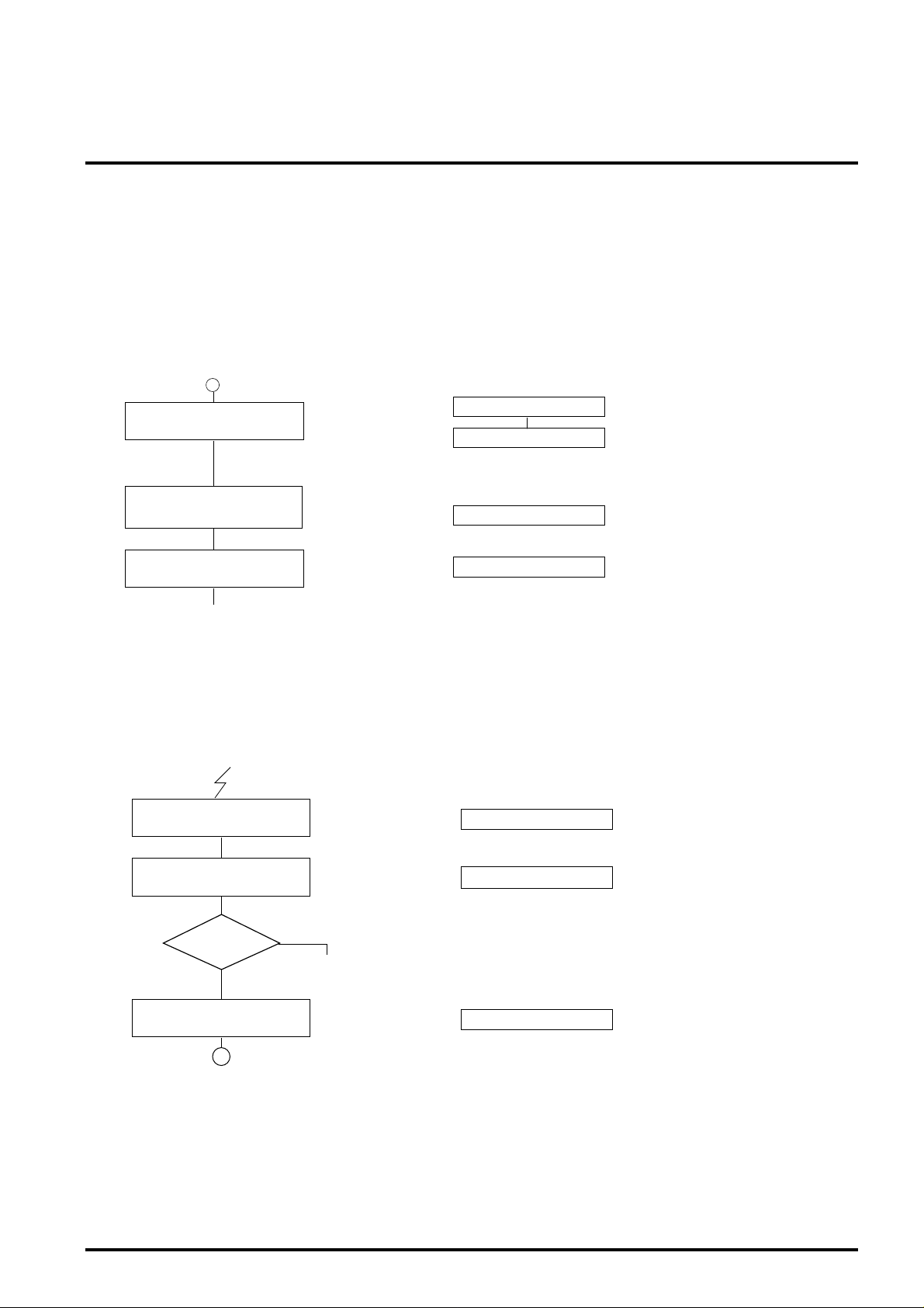
4. Register Setting Sequence
(1) Initialization sequence of built-in line memory and context table
RAM
This sequence is used to carry out initialization sequence (0
clear) of context table RAM after the initialization (Note) of the
built-in line memory by H/W reset.
When the initialization is unnecessary (the contents of the
current status table are directly used), this sequence is
unnecessary.
MITSUBISHI SEMICONDUCTOR (LSI)
M65762FP
QM-CODER
1
H/W reset,
context mode set up
Issue context table RAM
initialization command
Set interrupt enable
Context table RAM is initialized (0 clear) in this period.
The number of clocks required for initialization is as follows:
1024 +a[Clock]
(Occurrence of interrupt)
Set interrupt disable
SYS_REG:
SYS_REG:
CMD_REG:
IENB_REG:
IENB_REG:
d7 d0
;H/W reset bit ON0 0 0 0 0 0 0 1
0 0 0 0 0 0 0 0
* Period of H/W reset bit set to ON (time from when d0 = "1"
is written until d0 = "0" is written) requires 100 ns or more.
0 0 0 0 0 0 0 1
0 0 0 0 0 0 0 1
d7 d0
0 0 0 0 0 0 0 0
;H/W reset bit OFF
;Initializes context table RAM
;Process end interrupt enable
;Interrupt disable
Read out status register
(check the end of processing)
= 1 ?
(Error)
Y
End of initialization command
2
To 2)
(Note) Line memory is initialized by H/W reset to prepare the all white (0) data as a reference line to provide for the start of
coding/decoding process and to initialize LNTP bit (LNTP = 1) for typical prediction.
N
STAT_REG
CMD_REG:
– – – – – – – j
0 0 0 0 0 0 0 0
;j = End of processing
;End of initialization

MITSUBISHI SEMICONDUCTOR (LSI)
((
y)
j
(2) Stripe coding/decoding (without change in AT pixel position)/image data through processing sequence
2
;Cb, Cb = Bit width of code data bus
;Bs, Bx = Code data bus bit, byte swap
;Pb, Pi = Bit width of image data bus,
;mm = operation mode
(coding/decoding/through)
;Ob, Ob = Selection of head byte read-through
during decoding (0-3)
;Li = Selection of inhibition of line memory
initialization (Note)
;Tp = Typical prediction function ON/OFF
;aa,aaaaa = AT pixel position
;t = Template selection
Set System
(Set LSI mode)
Set Operation
mode
Set Parameter
(Template, context)
d7 d0
SYS_REG:
MOD_REG:
(Note) Set Li = 0 for the head stripe of single
PARA_REG:
Pb Pi Bx Bs 0 Cb Cb 0
Tp Li ObOb 0 0 m m
stripe or multi-stripe.
a a t a a a a a
M65762FP
QM-CODER
I/F selection
Set the number of pixels
Set the number of lines
Set marker code
Note)Required coding onl
Set scale-up/scale-down
Processing start command
(Coding/decoding/through)
Set interrupt enable
[Performs coding/decoding processing during this period.]---Inputs/outputs image data and coding data.
(Occurrence of interrupt)
Set interrupt disable
PEL_REG_L :
PEL_REG_H:
LSET_REG_L :
LSET_REG_H:
MSET_REG:
CONV_REG:
CMD_REG:
IENB_REG:
IENB_REG:
pel_l
0 0
0 0 0 HoHrVrHeVe
0 0 0 0 0 0 1 0
0 0 0 0 0 0 0 1
d7 d0
pel_h
lset_l
lset_h
mset
(Coding/decoding/through processing for a stripe)
0 0 0 0 0 0 0 0
;pel_l, pel_h =Number of pixels per 1 line
;lset_l, lset_h =Number of processing lines
mset = sets marker code byte
(SDNORM = 02h, SDRST = 03h)
;Ve, He = Selection of scale-up during
decoding
;Vr, Hr, Ho = Selection of scale-down
at time of coding
;Termination end processing
(coding/decoding/through)
Start command
;Process end interrupt enable
;Interrupt disable
Read out status register
(Check process for end.)
= 1 ?
Y
Decoding?
Y
(Decoding)
m = 1 ?
Y
(Marker detection)
Read marker code
((Note) At time of decoding only)
End
N
(Error)
N (Coding)
N (Marker not detected)
(Error)
STAT_REG:
MDET_REG:
– – – s – m – j
s = 0 ?
Y
End
mdet
;j = End of processing
;m = Marker detection
;s = SC counter over error
N (SC counter over)
(Error)
;mdet = Read marker code

(3) Stripe encoding/decoding (with change in AT pixel position) processing sequence
j
((
y)
MITSUBISHI SEMICONDUCTOR (LSI)
M65762FP
QM-CODER
2
Set System
(Set LSI mode)
Set Operation mode
Set Parameter
(Template, context)
Set the number of pixels
Set the number of lines
Set marker code
Note) Required coding onl
Set scale-up/scale-down
Processing start command
(Temporary stop processing)
Set interrupt enable
d7 d0
SYS_REG:
MOD_REG:
(Note) Set Li = 0 for single stripe or the head
PARA_REG:
PEL_REG_L :
PEL_REG_H:
LSET_REG_L :
LSET_REG_H:
MSET_REG:
CONV_REG:
CMD_REG:
IENB_REG:
Pb Pi Bx Bs 0 Cb Cb 0
Tp Li Ob Ob 0 0 0 m
stripe of multi-stripe.
a a t a a a a a
pel_l
0 0
0 0 0 HoHrVrHeVe
0 0 0 0 1 0 1 0
0 0 0 0 0 0 0 1
pel_h
lset_l
lset_h
mset
;Cb, Cb = Bit width of code data bus
;Bs, Bx = Code data bus bit, byte swap
;Pb, Pi = Bit width of image data bus, I/F
;m = operation mode (encoding/decoding)
;Ob, Ob = Selection of head byte read-through
;Li = Selection of inhibition of line memory
;Tp = Typical prediction function ON/OFF
;aa,aaaaa = AT pixel position
;t = Template selection
;pel_l, pel_h = Number of pixels per 1 line
;lset_l, lset_h = Number of processing lines
(Note) Set the number of processing lines to
mset = sets marker code byte
(SDNORM = 02h, SDRST = 03h)
;Ve, He = Selection of scale-up at time of
;Vr, Hr, Ho = Selection of scale-down at
;Temporary stop processing
(coding/decoding)
Start command
;Process end interrupt enable
selection
during decoding (0-3)
initialization (Note)
position change of AT pixel.
decoding
time of coding
[Performs coding/decoding processing during this period.]---Input/output first image data and coding data.
(Occurrence of interruption)
Set in the course
Processing start command
Repeat this routine (for the number of ATmoves - 1)
(Temporary stop processing)
Set interrupt disable
Read status register
Set final AT
Set AT pixel position
Set the number of lines
Set interrupt enable
(Note) At time of coding in the first processing, (number of lines of input image data) = (value set in the line
count set register) +1. During decoding, (number of lines in output image data) = (value set in the
line set register) - 1
d7 d0
IENB_REG:
STAT_REG:
Final set
PARA_REG:
LSET_REG_L:
LSET_REG_H:
CMD_REG:
IENB_REG:
0 0 0 0 0 0 0 0
– – p – – – – j
3
a' a' t' a' a' a' a' a'
lset_l
lset_h
0 0 0 0 1 0 1 0
0 0 0 0 0 0 0 1
;Interrupt disable
;Status check
=0, p=1; Temporary stop status
;Set change of AT pixel (a'a',a'a'a'a'a')
(Note) Template is not allowed to be
changed.
;lset_l,lset_h = Number of processing lines
(Note) Set the number of processing lines
ranging from processing restart to
change of AT pixel position
;Temporary stop processing
(encoding/decoding)
Start command
;Process stop interrupt enable
[Performs encoding/decoding process during this period.]---Inputs/outputs image data and coding data in the course.
(Note) During encoding in the course of processing, (number of lines in input image data) = (value set
in the line count set register). At time of decoding, (number of lines in output image data) =
(value set in the line count set register).

MITSUBISHI SEMICONDUCTOR (LSI)
j
M65762FP
QM-CODER
3
SET AT pixel position
Set number of lines
Processing start command
(Termination end processing)
Set interrupt enable
[Performs coding/decoding processing during this period.] --- Inputs/outputs final image data and coding data.
(Note) During coding in the final processing, (number of lines in input image data) = (value set in the line count
(Occurrence of interrupt)
Set interrupt disable
Read out status register
(Check end of processing.)
= 1 ?
Y
Decoding?
N
N(Encoding)
PARA_REG:
LSET_REG_L:
LSET_REG_H:
CMD_REG:
IENB_REG:
set register) – 1. During decoding, (number of lines in output image data) = (value set in the line count
set register) + 1.
IENB_REG:
STAT_REG:
(Error)
a" a" t a" a" a" a" a"
lset_l
lset_h
0 0 0 0 0 0 1 0
0 0 0 0 0 0 0 1
d7 d0
0 0 0 0 0 0 0 0
– – – s – m – j
;Set change in final AT pixel.
(a"a",a"a"a"a"a")
(Note) Template is not allowed to be changed.
;lset_l,lset_h = Number of processing lines
(Note) Enter the number of processing lines
ranging from restart of processing to the
final line.
;Termination end processing
(coding/decoding)
Start command
;Process stop interrupt enable
;Interrupt disable
;j = End of processing
;m = Marker detection
;s = SC counter over error
(Decoding)
Y
m = 1 ?
Y
(Marker detection)
Read out marker code
((Note) Decoding only)
End
(4) Load/store processing sequence of the context table RAM
This sequence is used to load or store context table RAM.
RAM load/store start command
[Stores (loads) the context table RAM during this period.
Context RAM data is stored (loaded) via buffer register.
Reading (writing) 2 bytes automatically increments the RAM address.
(Note) Reading (storing) operation and writing (loading) operation are not allowed to be done at a time.
End of RAM
load/store command
N(Marker not detected)
(Error)
MDET_REG:
CMD_REG:
CMD_REG:
s = 0 ?
Y
End
mdet
d7 d0
00000000
000000100
N (SC counter over)
(Error)
;mdet = Read marker code
;Starts to load/store context table RAM
;End of loading/storing RAM
Since the operation does not automatically stop,
be sure to write the load/store end command.

(5) Load/store processing sequence of line memory image data
j
2
Set System (Set LSI mode)
Set Operation mode
Set Parameter
(Selection of template)
SYS_REG:
MOD_REG:
*
PARA_REG:
d7 d0
Pb Pi Bx Bs Ds Cb Cb 0
Tp Li 0 0 LioLio 1 m
– – t – – – – –
MITSUBISHI SEMICONDUCTOR (LSI)
M65762FP
QM-CODER
;Cb, Cb = Bit width of code data bus
;Ds = Bit swap of image data bus
;Bs, Bx = Code data bus bit, byte swap
;Pb, Pi = Bit width of image data bus, I/F selection
;m = Operation mode (selection of through mode)
;Lio, Lio = 01 or 10 (selection of load or store)
;Li = 1 (selection of prohibition of line memory
initialization)
;Tp = Typical prediction function ON/OFF (Note 1)
;t = Selection of template
Set number of pixels
Set number of lines (= 2)
Set scale-up/scale down
Processing start command
(Load/store into line memory)
Set interrupt enable
[Performs loading/storing process during this period] --- Inputs (outputs) image data. (Transfer processing of image data for 2 lines)
(Occurrence of interrupt)
Set interruption disable
*
*
PEL_REG_L:
PEL_REG_H:
LSET_REG_L:
LSET_REG_H:
CONV_REG:
CMD_REG:
IENB_REG:
*Settings of template selection, number of pixels per line, selection of scale-up/scale-down and
typical prediction function must meet the settings at time of stripe coding/decoding to be carried
out after this.
IENB_REG:
pel_l
0 0
0 0 0 HoHrVrHeVe
0 0 0 0 0 0 1 0
0 0 0 0 0 0 0 1
d7 d0
pel_h
lset_l
lset_h
0 0 0 0 0 0 0 0
;pel_l, pel_h = Number of pixels per line
lset_l, lset_h = 2 (Number of processed lines)
(Note 2)
;Ve, He = Selection of scale-up during
decoding
;Vr, Hr, Ho = Selection of scale-down
during coding
;Load/store processing start command of
image data
;Process end interrupt enable
;Interrupt disable
Read out status register
(Check end of processing.)
= 1 ?
Y
End
Note 1) For ON/OFF bit of TP function in the image data processing, the ON/OFF bit of the
TP function just before coding/decoding shall be kept.
Note 2) In the image data load/store processing, be sure to set the number of transfer lines
to "2".
(The 1st line is data on the line (final line - 1) of the stripe. The 2nd line is data on
the last line of stripe.)
When a line stripe is adopted for the first stripe of the page in the image data store
processing, and read out line of the first line is outside data of stripe, the all white
data must used for replacement or the image data load function must be used in
advance to clear line memory.
N
(Error)
STAT_REG:
– – – – – – – j
;j = End of processing
Stripe
Head line
•
•
•
(Final line - 1) line
Final line
1st line
2nd line

MITSUBISHI SEMICONDUCTOR (LSI)
M65762FP
QM-CODER
(6) Total sequence of multi-stripe coding/decoding
For an image with a page consisting of more than one stripe or
Multi-stripe
coding/decoding
Initialization of built-in memory
and context table RAM
1st stripe coding/decoding
processing
End of processing
of all stripes?
Is previous stripe
SDNORM?
[case1]
Initialization of line memory and
context table RAM
Stripe coding/decoding
processing (Indication of line
memory initialization: Li = 0, AT
pixel = Default position (0))
Repetition of this routine (for the number of stripes - 1)
[Process (1)]
[process (2) or (3)]
N
(SDRST)
N
[Process (1)]
[Process (2) or (3)]
Y
End of page
Y
(SDNORM)
Y(Same plane)
[case2]
Stripe coding/decoding
processing (Prohibition of line
memory initialization: Li = 1, AT
pixel = Previous stripe taken
over)
[Process (2) or (3)]
plane, coding or decoding process must be carried out in units
of stripe after initialization.
(Note 1)
Since use of the host bus with 32/16-bit bus during coding adopts word
boundary, the end marker code may be followed by the pad bytes ('00')
of 1 to 3-byte. These pad bytes must be removed outside. (See
Section 2. (7).)
(Note 2)
When decoding of stripes starts at time of decoding, the head coding
data of SDE (stripe data entity) must be first entered. Read-through of
head byte is indicated, if necessary. (At time of end of decoding
stripes, the head block of coding data may be entered into LSI (FIFO)
or may not be arranged in the word boundary. Management is
therefore required outside.)
(Note 3)
The process of inter-stripe marker codes (ATMOVE, NEWLEN, etc.)
(insert at time of coding and detection/removal at time of decoding)
must be carried out outside.
Does the same plane
stripe continue?
N (Difference plane)
[case3]
Loading of image data of line
memory, and loading of context
table RAM
[Processes (4) and (5)]
Stripe coding/decoding
processing
(Prohibition of line memory
initialization: Li = 1, AT pixel =
Respecify)
[Process (2) or (3)]
Storing of image data of line
memory and storing of context
table RAM
[Processes (4) and (5)]
(Description)
If the end marker of the previous stripe is SDRST, the status must be
initialized for coding/decoding the next stripe. Start to carry out the
process of next stripe by returning the AT pixel position to the default
position after the initialization of built-in line memory and context table
RAM. [case 1]
If the termination marker of the previous stripe is SDNORM, the status
of the previous stripe must be taken over for coding/decoding the next
stripe. If the stripe of the same plane is continuously coded/decoded,
the AT pixel position takes over the final value of the previous stripe
and the process of the next stripe is to start without initializing line
(Example)
• Single plane, multi-stripe
Plane
1
23
Stripe
(Processes in numeric order)
4
memory and context table RAM to use the status of line memory
and context table RAM at the end of previous stripe for the next
stripe. [case 2]
On the other hand, since the status at the end of pre-stripe status
of the same plane must be respecified for the status of line memory
and context table RAM, line memory and context table RAM are to
be loaded into LSI to respecify the AT pixel position and to start
processing the next stripe when alternately coding/decoding stripes
of different planes. After coding/decoding of stripe, save line
memory and context table RAM for next stripe. [case 3]
• Multiple planes and multi-stripe
Plane 1
Plane 2
Plane 3
1
2
3
4
5
6
7
8
9
10
11
12

Timing Chart
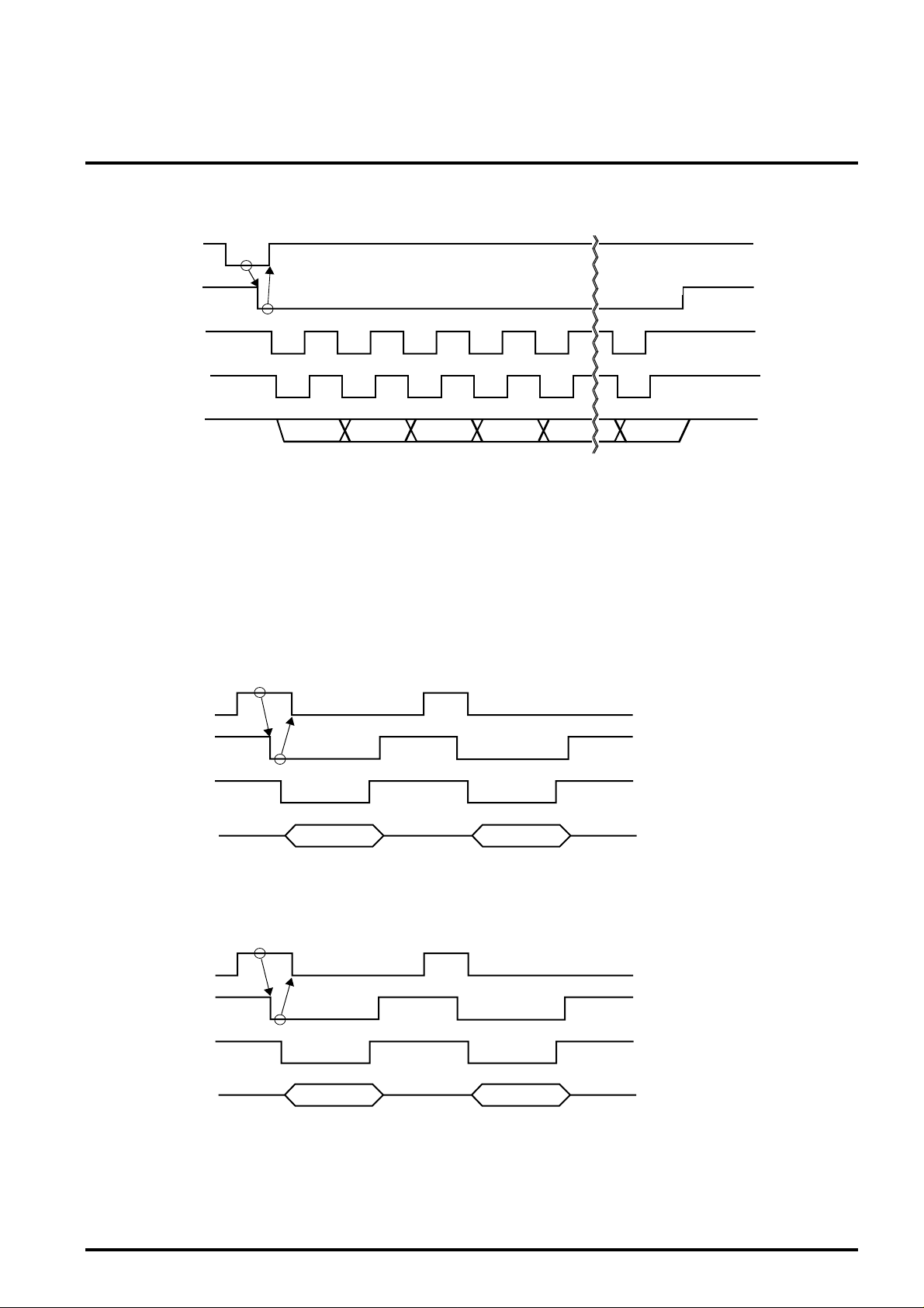
1. Host bus I/F
CS*
RD*
WR*
A0-3
D0-7
MITSUBISHI SEMICONDUCTOR (LSI)
M65762FP
QM-CODER
2. Code data I/F
(a) For 8-bit bus
CDRQ
CDAK*
CDRD*/CDWR*
CD0-7
(b) For 16-bit bus
CDRQ
CDAK*
CDRD*/CDWR*
CD0-15
Read access
(Note) For 16-bit bus, only the word access (CD0-15) is allowed.
Write access
(c) For 32-bit bus
CDRQ
CDAK*
CDRD*/CDWR*
CD0-31
(Note) For 32-bit bus, only the long word access (CD0-31) is allowed.
(Description)
CDRQ can be checked for being asserted (H) to assert (L) CDAK*.
Asserting (L) CDAK* negates (L) CDRQ.
Asserting (L) section of CDRD*/CDWR* must be included in the CDAK* asserting section (L).
3. Image Data I/F
/
/
(1) Serial image data I/F
PRDY*
PTIM*
PXCK*
PXCKO*
MITSUBISHI SEMICONDUCTOR (LSI)
M65762FP
QM-CODER
SVID*/RVID*
(Note) The above chart shows a timing for a line (N pixel/line).
(Description)
PRDY* can be checked for being asserted (L) to assert (L) PTIM*.
Asserting (L) PTIM* negates (H) PRDY*.
PXCKO* is an output of having gated PXCK* input with PTIM*.
The image data (SVID*/RVID*) is input/output in synchronization with PXCK* or PXCKO*.
(2) Parallel image data I/F
(a) 16-bit bus
PDRQ
PDAK*
PDRD*
PDWR*
PD0-15
1
234
5N
(Note) For 16-bit bus, only the word access (PD0-15) is allowed.
(b) 32-bit bus
PDRQ
PDAK*
PDRD*
PDWR*
PD0-31
(Note) For 32-bit bus, only the long word access (PD0-31) is allowed.
(Description)
PDRQ can be checked for being asserted (H) to assert (L) PDAK*.
Asserting (L) PDAK* negates (H) PDRQ.
Asserting (L) section of PDRD*/PDWR* must be included in the asserting section (L) of PDAK*.

System Configuration Example
1. Application Examples to Digital PPC
and FAX Hybrid Machine
MITSUBISHI SEMICONDUCTOR (LSI)
M65762FP
QM-CODER
Image
sensor
Printer
Making frame memory
unnecessary by using QM-Coder
Reduction/efficiency of
memory by QM-Coder
Binary
image
processing
Figure 5. Application Examples to Digital PPC and Fax Hybrid Machine
QM-Coder
(M65762FP)
QM-Coder
(M65762FP)
Code
memory
Disk unit
MPU
DMAC
Communication
control
High speed communication
by QM-Coder
2. Application Example to Printer
High Speed Transfer from PC/WS to Printer (LBP/UP), and
Reduction of Memory
PC/WS
Image data
file
High speed
communication with
QM coding data
Figure 6 Application Example to Printer
QM encoder
(H/W or S/W)
Printer (LBP)
Code memory
Reduction of memory
capacity with real-time
decoding
QM decoder
(M65762FP)
Recording

[Appendix A.1] JBIG Data Structure
B I E ;Bi-level Image Entity
B I H ;Bi-level Image Header
L
D
D
P
XD
YD
LD
MX
MY
Order
HITOLO
SEQ
ILEAVE
SMID
Options 1 ;option byte
LRLTWO
VLENGTH
TPDON
TPBON
DPON
DPPRIV
DPLAST
DPTABLE 0/1728 ;private DP table
B I D ;bi-level Image Data(( ) x N)
Flloating Marker Segments( a ~ c )
1
a AT move marker
b new-length marker
;lowest resolution layer
1
;finel resolution layer
1
;number of bit-planes
1
;dummy 0
1
;horizontal dimmension at highest resolution
4
;vertical dimmension at highest resolution
4
;number of lines per stripe at lowest resolution
4
;maximum horizontal offsets allowed for AT pixel
1
;maximum vertical offsets allowed for AT pixel
1
;order byte
1
b7-4;dummy 0
b3 ;resolution-order distinction
b2 ;progressive-versus-seqential distinction
b1 ;interleaving of multiple bit-planes
b0 ;indexed over stripe is in middle
b7 ;dummy 0
b6 ;lowest resolution-layer two line template
b5 ;NEWLEN(new vertical dimmension)marker enable
b4 ;differential-layer TP enable
b3 ;lowest-resolution-layer TP enable
b2 ;DP enable
b1 ;private DP table
b0 ;DP table last is to be reused
1
ESC
ATMOVE
AT
Y
τ X
τ Y
ESC
NEWLEN
YD
;FFh
1
;06h
4
;line in which an AT switch is to be made
1
;holizontal offset of the AT pixel
1
;vertical offset of the AT pixel
1
;FFh
1
;05h
4
;new YD
MITSUBISHI SEMICONDUCTOR (LSI)
M65762FP
QM-CODER
(it is present only if DPON=1, DPPRIV=1, DPLAST=0)
21
c comment marker
ESC
COMMENT
LC
comment
2
SDE ;Stripe Data Entry (Within the frame: LSI support range)
PSCD
ESC
SDNORM/SDRST
abort BID marker
ESC
ABORT
reserved marker
ESC
RESERVE
;FFh
1
;07h
1
;length in bytes of private comment
4
;contents of comment
L
C
;Protected Stripe Coded Data
=byte stuffed SCD(Stripe Code Data)
;FFh
1
;normal terminate(02h)
1
;/reset "state" for next SDE(03h)
1
;FFh
1
;04h
1
;FFh
1
;01h

MITSUBISHI SEMICONDUCTOR (LSI)
M65762FP
QM-CODER
[Appendix A.2] JBIG Probability Estimation Table
ST LSZ NLPS NMPS SWTCH ST LSZ NLPS NMPS SWTCH
10
11
12
13
14
15
16
17
18
19
20
21
22
23
24
25
26
27
28
29
30
31
32
33
34
35
36
37
38
39
40
41
42
43
44
45
46
47
48
49
50
51
52
53
54
55
56
0
1
2
3
4
5
6
7
8
9
0x5ald
0x2586
0x1114
0x080b
0x03d8
0x01da
0x00e5
0x006f
0x0036
0x001a
0x000d
0x0006
0x0003
0x0001
0x5a7f
0x3f25
0x2cf2
0x207c
0x17b9
0x1182
0x0cef
0x09a1
0x072f
0x055c
0x0406
0x0303
0x0240
0x01b1
0x0144
0x00f5
0x00b7
0x008a
0x0068
0x004e
0x003b
0x002c
0x5ae1
0x484c
0x3a0d
0x2ef1
0x261f
0x1f33
0x19a8
0x1518
0x1177
0x0e74
0x0bfb
0x09f8
0x0861
0x0706
0x05cd
0x04de
0x040f
0x0363
0x02d4
0x025c
0x01f8
14
16
18
20
23
25
28
30
33
35
10
12
15
36
38
39
40
42
43
45
46
48
49
51
52
54
56
57
59
60
62
63
32
33
37
64
65
67
68
69
70
72
73
74
75
77
78
79
48
50
50
51
52
53
54
1
9
10
11
12
13
13
15
16
17
18
19
20
21
22
23
24
25
26
27
28
29
30
31
32
33
34
35
37
38
39
40
41
42
43
44
45
46
47
48
49
50
51
52
53
54
55
56
57
1
2
3
4
5
6
7
8
9
9
1
0
0
0
0
0
0
0
0
0
0
0
0
0
1
0
0
0
0
0
0
0
0
0
0
0
0
0
0
0
0
0
0
0
0
0
1
0
0
0
0
0
0
0
0
0
0
0
0
0
0
0
0
0
0
0
0
57
58
59
60
61
62
63
64
65
66
67
68
69
70
71
72
73
74
75
76
77
78
79
80
81
82
83
84
85
86
87
88
89
90
91
92
93
94
95
96
97
98
99
100
101
102
103
104
105
106
107
108
109
110
111
112
0x01a4
0x0160
0x0125
0x00f6
0x00cb
0x00ab
0x008f
0x5b12
0x4d04
0x412c
0x37d8
0x2fe8
0x293c
0x2379
0x1edf
0x1aa9
0x174e
0x1424
0x119c
0x0f6b
0x0d51
0x0bb6
0x0a40
0x5832
0x4d1c
0x438e
0x3bdd
0x34ee
0x2eae
0x299a
0x2516
0x5570
0x4ca9
0x44d9
0x3e22
0x3824
0x32b4
0x2e17
0x56a8
0x4f46
0x47e5
0x41cf
0x3c3d
0x375e
0x5231
0x4c0f
0x4639
0x415e
0x5627
0x50e7
0x4b85
0x5597
0x504f
0x5a10
0x5522
0x59eb
55
56
57
58
59
61
61
65
80
81
82
83
84
86
87
87
72
72
74
74
75
77
77
80
88
89
90
91
92
93
86
88
95
96
97
99
99
93
95
101
102
103
104
99
105
106
107
103
105
108
109
110
111
110
112
112
58
59
60
61
62
63
32
65
66
67
68
69
70
71
72
73
74
75
76
77
78
79
48
81
82
83
84
85
86
87
71
89
90
91
92
93
94
86
96
97
98
99
100
93
102
103
104
99
106
107
103
109
107
111
109
111
0
0
0
0
0
0
0
1
0
0
0
0
0
0
0
0
0
0
0
0
0
0
0
1
0
0
0
0
0
0
0
1
0
0
0
0
0
0
1
0
0
0
0
0
0
0
0
0
1
0
0
0
0
1
0
1

MITSUBISHI SEMICONDUCTOR (LSI)
M65762FP
QM-CODER
[Appendix B] Timing Characteristics
1. Host bus I/F
RESET*
t0
CS*
t1
A0-3
t3 t5
RD*
WR*
D0-7
t4
t6 t7
Output
2. Code data I/F
CDRQ
t20
CDAK*
t21
CDRD*
CDWR*
CD0-31
t24
t26 t27
Output
t22
Conditions:VDD=5V±5%
t2
t13 t15
t11
t14
t16
Input
t31
t34
t36 t37
t32
Input
C=50pF
Ta=0-70°C
t12
t17

MITSUBISHI SEMICONDUCTOR (LSI)
M65762FP
QM-CODER
Table B. 1 Host Bus I/F Timing Characteristics
Abbreviation
t0
t1
t2
t3
t4
t5
t6
t7
t11
t12
t13
t14
t15
t16
t17
RESET* assert time
CS* setup time to RD* assert
CS* hold time to RD* negate
A0-3 setup time to RD* assert
RD* assert time
A0-3 hold time to RD* negate
D0-7 output determination time to RD* assert
D0-7 output hold time to RD* negate
CS* setup time to WR* assert
CS* hold time to WR* negate
A0-3 setup time to WR* assert
WR* assert time
A0-3 hold time to WR* negate
D0-7 input setup time to WR* negate
D0-7 input hold time to WR* negate
Parameter
Table B. 2 Timing Characteristics of Code Data Bus I/F
Abbreviation
t20
t21
t22
t24
t26
t27
CDRQ negate time to CDAK* assert
CDAK* setup time to CDRD* assert
CDAK* hold time to CDRD* negate
CDRD* assert time
CD0-31 output determination time to CDRD* assert
CD0-31 output hold time to CDRD* negate
Parameter
(Unit: ns)
Timing conditions
Min Typ
100
15
15
15
20
15
0
0
15
15
15
15
15
20
5
Timing conditions
Min Typ Max
15
15
20
0
0
Max
-
-
-
-
-
-
-
20
-
20
-
-
-
-
-
-
-
-
15
-
-
-
-
20
-
20
-
-
-
-
-
-
-
-
-
-
-
-
-
-
-
-
t31
CDAK* setup time to CDWR* assert
t32
CDAK* hold time to CDWR* negate
t34
CDWR* assert time
t36
CD0-31 input setup time to CDWR* negate
t37
CD0-31 input hold time to CDWR* negate
15
15
15
15
-
-
-
-
5
-
-
-
-
-
-

3. Image data I/F
(1) Serial image data I/F
PRDY*
PTIM*
PXCK*
PXCKO*
RVID*
SVID*
t46
t50
t56
t40
t41
MITSUBISHI SEMICONDUCTOR (LSI)
M65762FP
QM-CODER
t45
t43
t47
t49
t51
1
t57
1
2
2
t44
3
3N
t42
t48
N
(2) Parallel image data I/F
PDRQ
PDAK*
t61
PDRD*
PDWR*
PD0-31
t60
t62
t64
t66 t67
Output
t71
t76
4. Master clock input frequency (LSI operating frequency)
Mx
MCLK
Mh
Ml
t72
t74
t77
Input

MITSUBISHI SEMICONDUCTOR (LSI)
M65762FP
QM-CODER
Table B. 3 Timing Characteristics of Image Data I/F
Abbreviation
t40
t41
t42
t43
t44
t45
t46
t47
t48
t49
t50
t51
t56
t57
t60
t61
t62
t64
t66
t67
PRDY* negate time to PTIM* assert
PTIM* setup time to PXCK* fall
PTIM* hold time to PXCK* rise
PXCK* high time
PXCK* low time
PXCK* cycle
RVID* output determination time to PXCK* fall
RVID* output change time to PXCK* fall
RVID* negate time to PTIM* negate
PXCKO* delay time to PXCK*
RVID* output determination time to PXCKO* fall
RVID* output change time to PXCKO* fall
SVID* setup time to PXCK* rise
SVID* hold time to PXCK* rise
PDRQ negate time to PDAK* assert
PDAK* setup time to PDRD* assert
PDAK* hold time to PDRD* negate
PDRD* assert time
PD0-31 output determination time to PDRD* assert
PD0-31 output hold time to PDRD* negate
Parameter
Timing conditions
Min Typ
-
15
15
10
10
25
10
10
15
15
20
-
-
-
-
-
-
-
-
-
0
-
-
-
-
-
-
-
-
-
-
-
-
-
-
0
-
0
-
(Unit: ns)
Max
20
-
-
-
-
20
20
10
12
12
-
-
15
-
-
20
20
t71
PDAK* setup time to PDWR* assert
t72
PDAK* hold time to PDWR* negate
t74
PDWR* assert time
t76
PD0-31 input setup time to PDWR* negate
t77
PD0-31 input hold time to PDWR* negate
Table B. 4 Master Clock Frequencies
Parameter
MCLK cycle (Mx)
MCLK high level time (Mh)
MCLK low level time (Ml)
Timing conditions
Min Typ
25
10
10
15
15
15
15
(Unit: ns)
Max
frequency
Max
-
-
-
-
-
40MHz
-
-
-
-
-
5
-
-
-
-
-
-
 Loading...