

MITSUBISHI ICs (TV)
M65677FP
DIGITAL NTSC/PAL ENCODER
DESCRIPTION
The M65677FP encodes CCIR601 or CCIR656 format Y/Cb/Cr data
into analog NTSC and PAL video signals, including Digital Signal
Processing functions such as Closed Caption encoding, Overlay
OSD, Anti Video Copy Processing (Note1) e.t.c. It also includes
peripheral processing function such as 10bit DAC e.t.c., so that low
cost and compact system can be realized.
FEATURES
Macrovision’s video anti copy process
•
Rev 7.01 supported (Note1)
•
Overlay CGMS signal on line 20/283 for 525/60 (Note3)
•
Generate CRCC for CGMS Signal
•
Overlay WSS signal on line 23 for 625/50 (Note4)
•
Color adjustment (TINT/color control)
•
NTSC, B/G PAL or MPAL Video Outputs
•
Component Y/C Video (S-Video) and CVBS or Y/U/V Outputs
•
Supporting CCIR601 and CCIR656 format data
•
Closed Caption Manager on line 21/284 for NTSC
•
Generate ODD parity for Closed Caption Manager
•
H/V Sync and Composite generating
•
Overlay Digital OSD Supporting Y/Cb/Cr 4:4:4
•
Over sampling Filter
•
2ch 10bit DAC and 3ch 6dB Amp (Note2)
•
3.3V I/O interface
2
•
I
C Bus Interface for Controls
•
Power down mode
Note
(Note1): This device is protected by U .S . patent numbers 4631603,
4577216 and 4819098 and other intellectual property
rights. The use of Macrovision Corporation's copy
protection technology in the device must be authorized by
Macrovision and is intended for home and other limited
pay-par-view uses only, unless otherwise authorized in
writing by Macrovision. Reverse engineering or
disassembly is prohibited.
P-P
(Note2): 6dB Amp max. output is 1.0V
.
(Note3): Copy Generation Management System-A (IEC1880)
(Note4): Wide Screen Signaling (ETS300 294)
APPLICATION
DVB, DVD , Digital CATV, Video CD
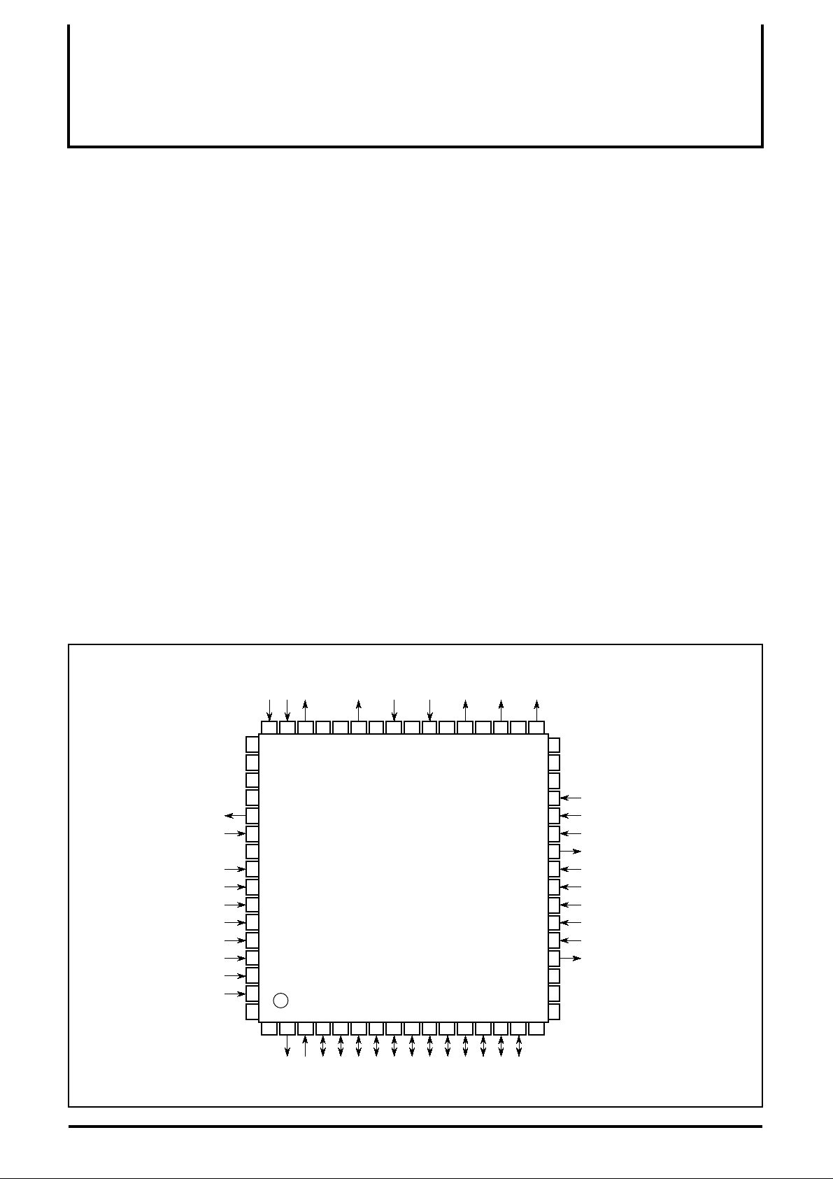
PIN CONFIGURATION (TOP VIEW)
Yref
47
48
Ycomp
49
50
N.C.
51
DV
DD1
DVSS1
52
DVSS2
DV
DD2
53
54
55
56
57
58
59
60
61
62
63
64
2
1
SS2
DV
X out
X in
PXD7
PXD6
PXD5
PXD4
PXD3
PXD2
PXD1
PXD0
Cref
DAY
46
3
PXCLK
DVASEL
SS1
AV
AVDD1
454443
5
4
VD
HD
DAC
C in
Ccomp
N.C
41
403938
42
M65677FP
8
7
VD8
VD7
9
VD6
6
VD9
Outline 64P6N-A
Y in
DD2
AV
101112
VD5
VD4
Y
37
VD3
CVBS
SS2
AV
363534
131415
VD2
VD1
N.C.
VD0
33
16
C
SS2
DV
32
31
30
29
28
27
26
25
24
23
22
21
20
19
18
17
N.C.
N.C.
DV
DD1
TEST
SCL
SDA
ACK
RESET
Master/slave
OSD2
OSD1
OSD0
OSDCK
DV
SS1
DVDD1
DVDD2
NC : NO CONNECTION
1
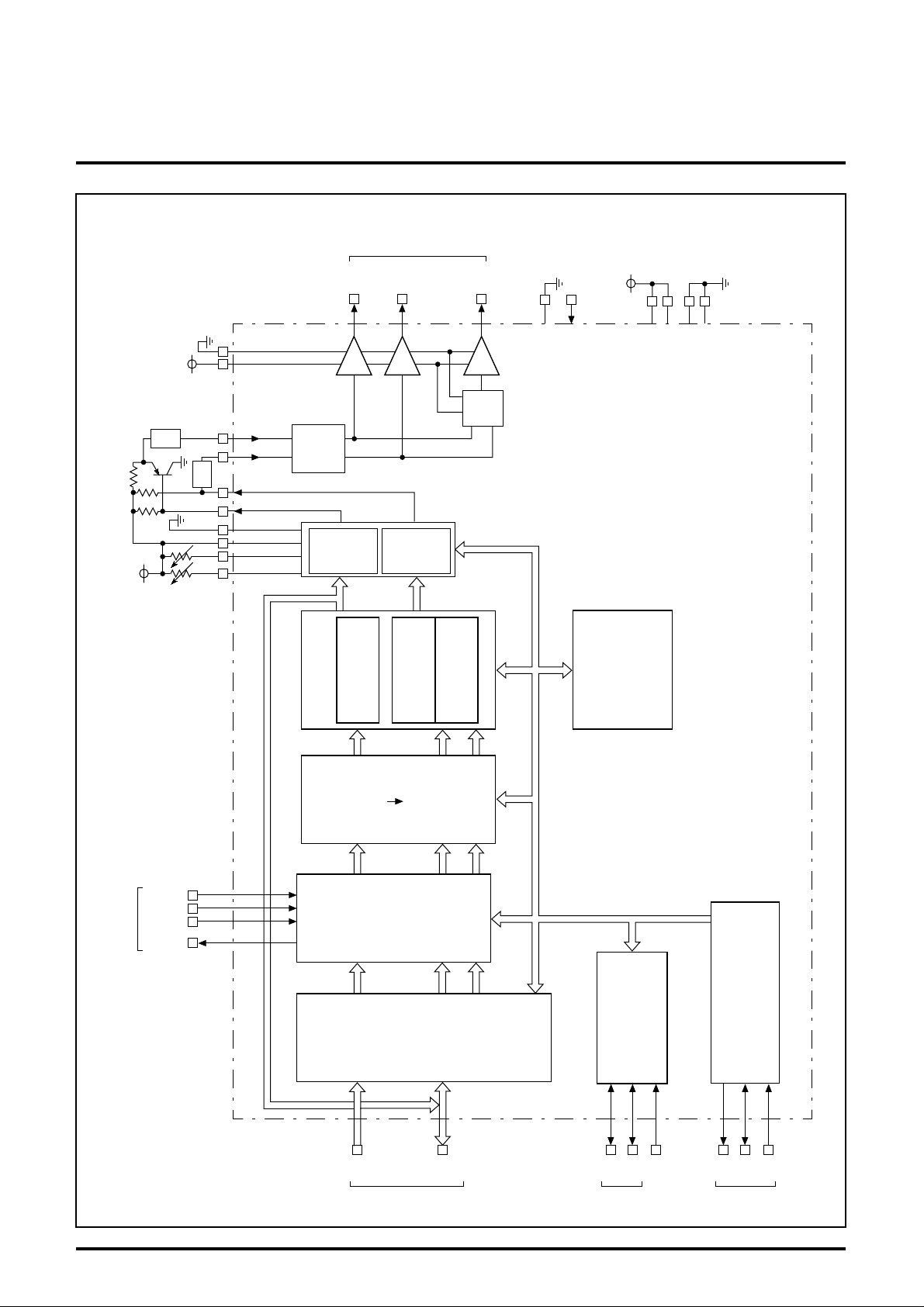
BLOCK DIAGRAM
AVSS2
AVDD2
Yin
LPF
Cin
DAC
AVss1
Y ref
C ref
DAY
AVdd1
BPF
MITSUBISHI ICs (TV)
M65677FP
DIGITAL NTSC/PAL ENCODER
Video
output
DVdd1(X2)
DVss2(X2)
DVss1(X2)
&
Clamp
bias
DAC
Y
6dB
C
6dB
DAC
CVBS
6dB
MIX
Y/C
TEST
RESET
DVdd2(X2)
OSD2
OSD1
OSD0
OSDCK
OSD Control I/F
Y/U
Manager
Closed Caption
Y
Y/Cb/Cr
Y
OSD
Interface
Y
C/V
Manager
CGMS/WSS
U
Y/U/V
Cb
Cb
Input
Interface
ENCODE
V
Cr
Cr
Anti Copy
Processing
Sync Processing
serial interface
Y
PXD [7:0]
CCIR601 or 656 Pixel
Data from MPEG decoder
VD [9:0]
VD
HD
From/To
MPEG decoder
Master
/Slave
ACK
SDA
From micro
controler
SCL
2
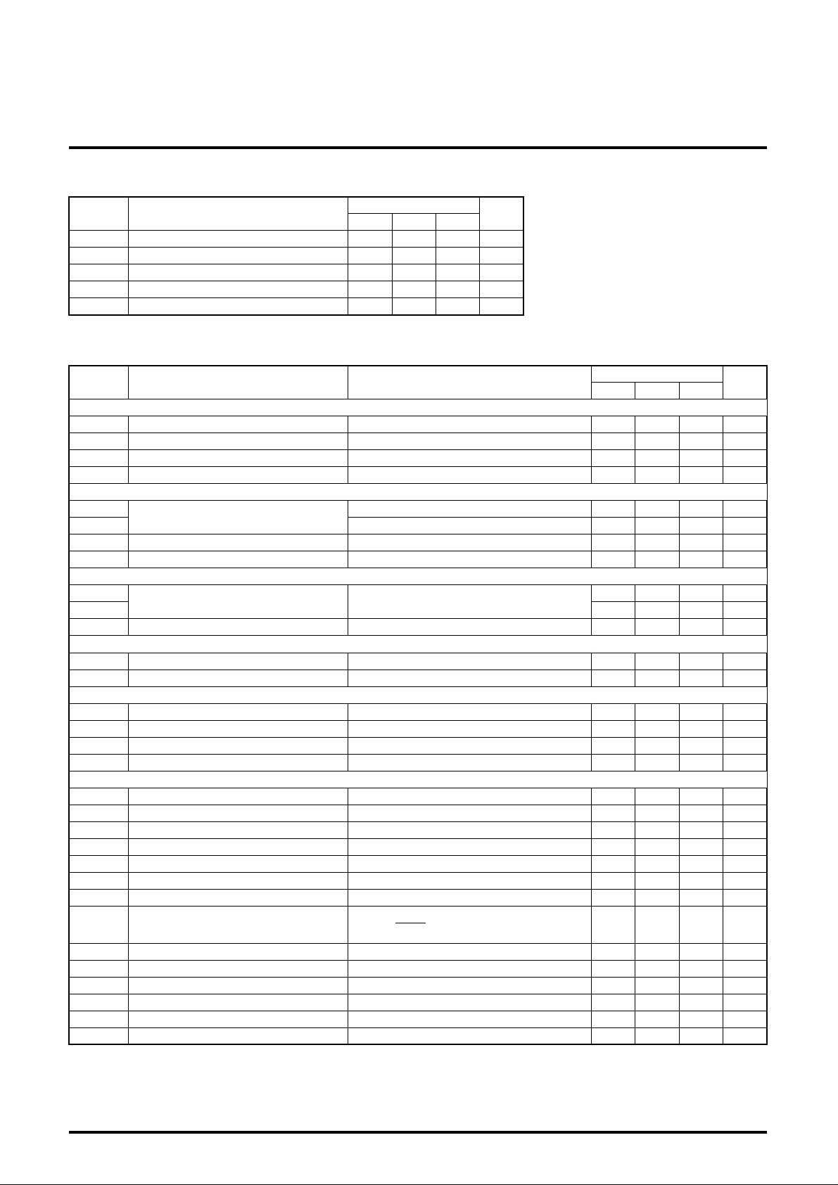
ABSOLUTE MAXIMUM RATINGS
Symbol Parameter
V
DD
V
I
V
O
T
a
T
stg
Supply voltage -0.3 4.5 V
Digital input voltage -0.3
Digital output voltage -0.3
Operating temperature -20 +25 +75 ° C
Storage temperature -40 +125 ° C
± 15 µ
| <1 µ
±
±
MITSUBISHI ICs (TV)
M65677FP
DIGITAL NTSC/PAL ENCODER
Limits
Min. Typ. Max.
DD
V
V
DD
+0.3
+0.3
Unit
V
V
RECOMMENDED OPERATING CONDITION
(Ta=25 ° C, DV
Symbol Parameter Test conditions
DD
=AV
DD
=3.3V, DV
SS
=AV
SS
=0V, unless otherwise noted)
Min. Typ. Max.
Limits
Supply
DDX
DV
AV
DI
AI
DDX
DD
DD
Digital supply voltage 3.0 3.3 3.6 V
Analog supply voltage 3.15 3.3 3.45 V
Digital current consumption 0 45 mA
Analog current consumption 0 55 mA
Digital input
IL
V
IH
V
IL
IL
I
/I
I
C
Input voltage
Input leakage current DV
Input capacitance f=1MHz, V
DD
DV
=3.0V 0 0.8 V
DD
DV
=3.6V 2.5 3.6 V
DD
I
=3.0V , V
=0V or V
DD
=0V 7 15 pF
I
=3.6V
Digital output
OL
V
OH
V
O
C
2
I
C bus
I
O
I
OZ
Output voltage DV
DD
=3.3V, | I
Output capacitance f=1MHz, V
Output current DV
Output leakage current (off) DV
=3.0V , V
DD
=3.6V , V
DD
O
A
DD
=0V 7 15 pF
=0.4V 4.0 mA
IL
=0V or V
I
=3.6V
I
3.25 V
0.05 V
± 15 µ A
D/A converter
Res Resolution 10 Bit
INL Integral non-linearity error
DNL Differential non-linearity error
Vf
SMAX
Maximum output amplitude 1.5 V
2.0 LSB
1.0 LSB
6-dB amplifier
R
G
G
DR
DR
bias
V_YC
V_CV
in
out
Bias resistor 7.5 10.0 11.5 k Ω
Output gain (Y/C) 5.50 6.00 6.50 dB
Output gain (CVBS) 5.10 6.00 6.85 dB
Input dynamic range 0.8 V
Output dynamic range 1.6 V
Iyich Yin clamp charge current -12 -26 -50 µ A
Iyids Yin clamp discharge current 0.26 0.65 1.80 µ A
Ryicl Yin clamp discharge current 20 0.65 70 –
Ryicl= -
Iyich
Iyids
Vyicl Yin input clamp voltage 0.45 0.50 0.55 V
Vyocl Y output clamp voltage 0.40 0.50 0.60 V
Vcvcl CVBS output clamp voltage 0.30 0.50 0.70 V
Vcin Cin input bias voltage 0.95 1.00 1.05 V
Vcob C output bias voltage 0.90 1.00 1.10 V
Iamp Output current 1.00 mA
Unit
A
P-P
P-P
P-P
3

DESCRIPTION OF PIN
Pin No. Pin name Type Function
1DV
SS2
2 PXCLK O
3DVA
SEL
4 HD I/O
5 VD I/O
6 VD9
7 VD8
8 VD7
9 VD6
10 VD5
11 VD4
12 VD3
13 VD2
14 VD1
15 VD0
16 DV
17 DV
18 DV
19 DV
SS2
DD2
DD1
SS1
20 OSDCK O
21 OSD0
22 OSD1
23 OSD2
24 Master/Slave I
25 RESET I Initializing reset. "LOW" is active.
26 ACK O Acknowledge line (Open drain output).
27 SDA I/O Serial data line/Acknowledge line (Open drain output).
28 SCL I Serial clock line.
29 TEST I
30 DV
DD1
31 N.C. No connection.
32 N.C. No connection.
33 C O
34 N.C. No connection.
35 CVBS O
36 AV
SS2
37 Y O
38 AV
DD2
39 Yin I
40 N.C. No connection.
41 Cin I
Supply Digital ground for the I/O.
Reference clock for input pixel data.
The clock frequency is 27.0MHz.
2
I
C slave address setting.
I
"Low" is for the address of 40h, "High" is for the address of 42h.
Horizontal sync signal input or output.
It is an input and output in the slave and master mode, respectively.
Vertical sync input or output. Or OddEven signal output.
It is an input and output in the slave and master mode, respectively.
Video data outputs.
I/O
In the Y/U/V output mode, the output is the 10-bit digital luma signal with a composite sync.
VD9 is MSB and VD0 is LSB.
Supply Digital ground for the I/O.
Supply Digital supply for the I/O.
Supply Digital supply for the internal logic.
Supply Digital ground for the internal logic.
The reference clock for an external OSD microcontroller.
The frequency is 13.5MHz or 6.25MHz, alternated by the I
The color look-up table address input.
I
MSB and LSB is OSD2 and OSD0, respectively.
Synchronizing mode selection.
"Low" is for the slave mode.
"High" is for the master mode.
For testing.
It should be grounded during an actual use.
Supply Digital supply for the internal logic.
The analog chroma output from a 6dB amplifier.
P-P
The output amplitude is 1.0V
(typ.), while the input is 0.5V
The analog composite video signal from a 6dB amplifier.
The output amplitude is 1.24V
P-P
Supply Analog ground for 6dB amplifiers.
The analog luma output from a 6dB amplifier.
(typ.), while input is 0.6V
The output amplitude is 1.2V
P-P
Supply Analog supply for 6dB amplifiers.
The analog luma input from an external LPF.
This input has bias circuit. The signal must input via a capacitor.
The analog chroma input from an external LPF.
This input has bias circuit. The signal must input via a capacitor.
(typ.).
MITSUBISHI ICs (TV)
M65677FP
DIGITAL NTSC/PAL ENCODER
2
C bus control.
P-P
.
.
P-P
4

MITSUBISHI ICs (TV)
M65677FP
DIGITAL NTSC/PAL ENCODER
DESCRIPTION OF PIN
Pin No. Pin name Type Function
42 Ccomp I
43 DAC O
44 AV
45 AV
46 DAY O
47 Cref I
48 Yref I
49 Ycomp I
50 N.C. No connection.
51 DV
52 DVSS1 Supply Digital ground for the internal logic.
53 Xout O
54 Xin I
55 DV
56 PXD7
57 PXD6
58 PXD5
59 PXD4
60 PXD3
61 PXD2
62 PXD1
63 PXD0
64 DVDD2 Supply Digital supply for the I/O.
DD1
SS1
DD1 Supply Digital supply for the internal logic.
SS2 Supply Digital ground for the I/O.
(cont.)
Phase compensation for chroma or V output DAC.
It should be connected to the analog ground via a capacitor.
Chroma or V signal output.
The DAC output should be connected to the analog supply via a load resistor (R
The output amplitude is set up by reference resistor (Rref) and RL.
Supply Analog supply for DACs.
Supply Analog ground for DACs.
Luma or U signal output.
It should be connected to the analog supply via a load resistor (RL).
The output amplitude is set up by reference resistor (Rref) and RL.
A reference current source for chroma or V signal output DAC.
It should be connected to the analog supply via a reference resistor (Rref).
A reference current source for Y or U DAC.
It should be connected to the analog supply via a reference resistor (Rref).
Phase compensation for Y or U DAC.
It should be connected to the analog ground via a capacitor.
System clock output.
It must be in no connection except for a connection to a X'tal oscillator.
System clock input.
The clock frequency is only 27.0MHz.
Pixel data inputs.
The acceptable video data are;
• multiplexed video data (Y/Cb/Cr) including timing reference code of SAV and EAV, defined in
I
CCIR Rec656
• multiplexed video data (Y/Cb/Cr) defined in CCIR Rec601
MSB and LSB is PXD7 and PXD0, respectively.
).
L
5

APPLICATION EXAMPLE
(CCIR656 I/F, Y/C/CVBS Output Mode)
0.01µ
47µ
27MHz
16M
47µ
0.01µ
SDRAM
0.1µ
DD
AVss
AV
Ccomp
TEST
Master/Slave
DVASEL
DVSS
DV
DD
X out
X in
47µ
0.01µ
VSS
VDD
CLK in
27MHz
XO
10k
0.1µ
Cref
Ycomp
VD(9:0)
Stage
Filter
10k
200
Yref
DAC
Digital
NTSC/PAL
Encoder
M65677FP
PXD(7:0)
PXCLKHDVD
8
PXD
PXCLK
MPEG2
System/
Video/Audio
Decoder
M65773FP
BCLK
BD
BDEN
Stage
Filter
200
0.1µ
C in
DAY
VSYNC
HSYNC
BDREQ
Y
757575
220µ
75Ω
Driver
2.2µ
2.2µ
Y
Y in
RESET
OSD(2:0)
OSDCK
ACK
SDA
SCL
SCL
SDA/ACK
RESET
AO0
AO1
AO2
AO3
LRCLK
DOCLK
DACCLK
ACLKO
ACLKI
BDER
C
0.1µ
C
CVBS
0.1µ
2.2µ
CVBS
MITSUBISHI ICs (TV)
M65677FP
DIGITAL NTSC/PAL ENCODER
220µ
47µ
0.01µ
3.3k
R/G/B
3
OSC1
OSD micro
computer
M35041
VDD
HDVDCS
RESET
VSS
SCK
SIN
Audio out (L)
Audio out (R)
Lch
Rch
Audio
DAC
LRCIN
DIN
XTI
BCKIN
8
BD
RCLK
BDEN
Chanel
Decoder
: 3.3V Power Supply (for Digital/Analog)
: 5.0V Power Supply (for Analog)
BDREQ
BDER
3.3k
CS
SCK
RESET
Host
CPU
SIN
Units Resistance : Ω
Capacitance : F
6
 Loading...