

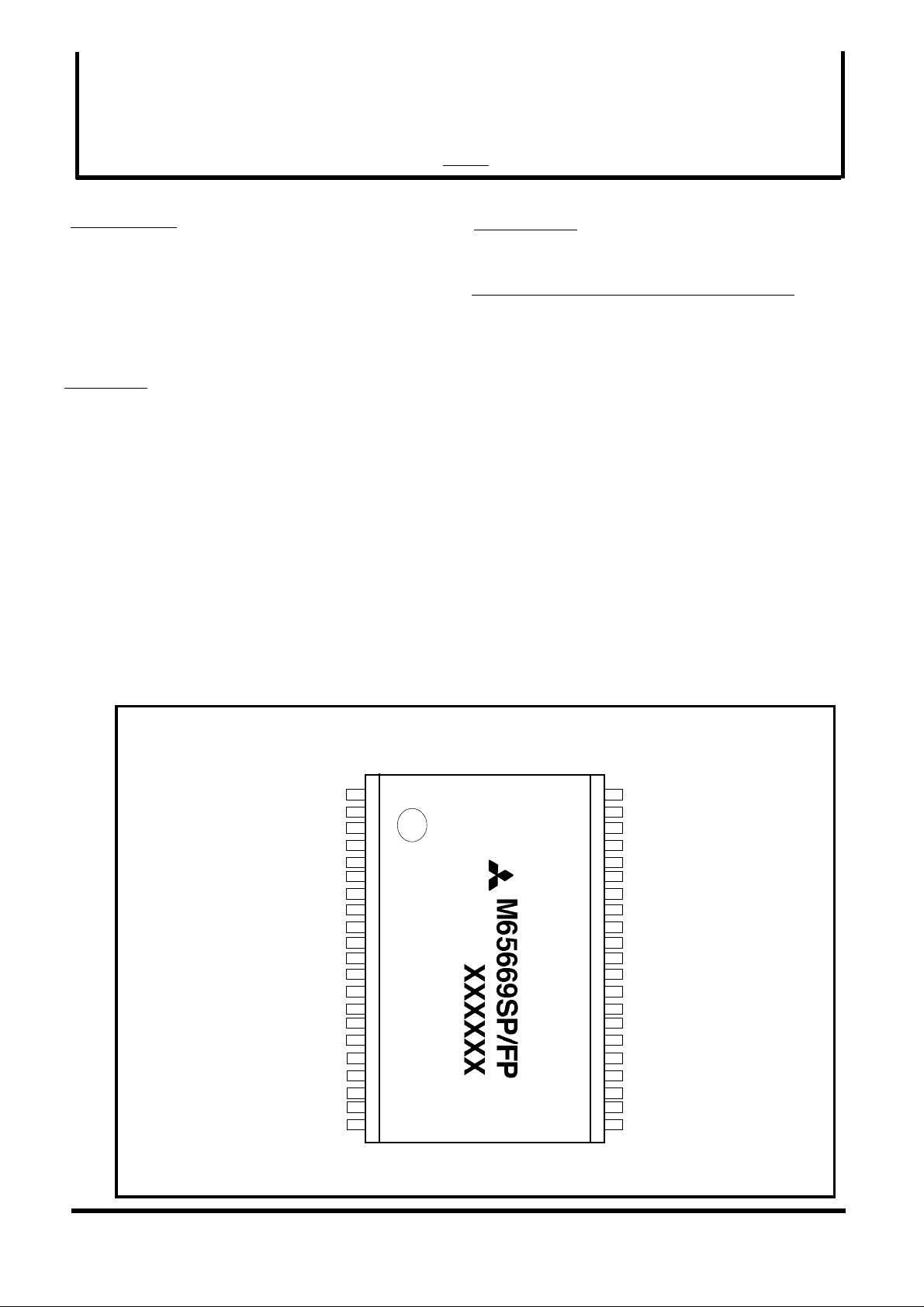
M65669SP/FP
PRELIMINARY
NTSC, PAL-M, PAL-N color TV
*1 : Include pin capacitance ( 7 pF )
PIN CONFIGURATION (TOP VIEW)
Notice ; This is not the final specification.
Some of information in this document are
subject to changes.
V3.1
MITSUBISHI DIGITAL TV ICs
PICTURE-IN-PICTURE
SIGNAL PROCESSING
DESCRIPTION
The M65669SP/FP is a PIP (Picture in Picture) signal
processing LSI, whose sub-picture input is composite
signal for NTSC, PAL-M, and PAL-N. The built-in field
memory (144k-bit RAM) , V-chip data slicer and analog
circuitries lead the high quality PIP system low cost and
small size.
FEATURES
* Built-in 144k-bit field memory ( sub-picture data storage)
* Internal V-chip data slicer (for sub-picture)
* Vertical filter for sub-picture ( Y signal )
* Single sub-picture ( selectable picture size : 1/9 , 1/16 )
* Sub-picture processing specification ( 1/9 , 1/16 size) :
Quantization bits Y, B-Y, R-Y : 6 bits
Horizontal sampling 229 pixels ( Y ) , 57 pixels ( B-Y, R-Y )
Vertical lines 69/ 52 lines
* Frame ( sub-picture ) on/off
* Built-in analog circuits :
One 8-bit A/D converter ( for sub-picture signal)
Three 8-bit D/A converters ( for Y, U and V of sub-picture )
Sync-tip-clamp, VCXO ... etc..
* IIC BUS control ( parallel/serial control) :
PIP on/off , Frame on/off ( programmable luma level),
Sub-picture size ( 1/9, 1/16 ),
PIP position ( free position ), Picture freeze ,
Y delay adjustment, Chroma level, Tint, Black level,
Contrast ...etc..
APPLICATION
RECOMMENDED OPERATING CONDITIONS
Supply voltage range ---------------------------------- 3.1 ~ 3.5 V
Operating frequency --------------------------------- 14.32 MHz
Operating temperature --------------------------------- -10 ~ 70 deg.
Input voltage (CMOS interface) "H" ----- VDD x 0.7 ~ VDD V
"L" ----- 0 ~ VDD x 0.3 V
Output current ( output buffer ) ------------------- 4 mA ( MAX )
Output load capacitance --------------------------- 20 pF ( MAX ) *1
Circuit current ---------------------------------------- - mA
NOTICE: Connect a 0.1µF or larger capacitor between VDD and VSS pins.
Block diagram & Application examples
Shown next pages
SWM
ACK
SDATA
SCLK
DVdd
DVss
BGPS
SCK
BGPM
FSC
TEST5
TEST6
SWMG
RESET
DVdd
DVss
MCK
CSYNCS
AVss(ad)
Vrb
Vrt
1
2
3
4
5
6
7
8
9
10
11
12
13
14
15
16
17
18
19
20
21
42
AVss(ana)
41
ADJ_Usub
40
Vdd(da)
YOUT
39
ADJ_Ysub
38
37
UOUT
36
ADJ_Vsub
35
VOUT
34
TESTEN
33
VD
32
HD
31
AVss(vcxo)
30
X'tal(P-N)
29
X'tal(P-M)
28
X'tal(NT)
27
BIAS
26
Filter
25
AVdd(vcxo)
24
AVdd(ad)
23
Vin(Sync sepa.)
22
Vin(ad)
Outline 42 Pin SDIP Package (M65669SP)
Outline 0.8mm pitch 42 Pin SOP Package (M65669FP)
( / )
15
1
M65669SP/FP
PRELIMINARY
Notice ; This is not the final specification.
Some of information in this document are
subject to changes.
BLOCK DIAGRAM
V3.1
MITSUBISHI DIGITAL TV ICs
PICTURE-IN-PICTURE
SIGNAL PROCESSING
Y OUTPUT
U OUTPUT
V OUTPUT
PIP SW
Sub picture
Main HD
Main VD
( / )
2
15
SCL
SDA
M65669SP/FP
PRELIMINARY
Notice ; This is not the final specification.
Some of information in this document are
subject to changes.
V3.1
MITSUBISHI DIGITAL TV ICs
PICTURE-IN-PICTURE
SIGNAL PROCESSING
ABSOLUTE MAXIMUM RATINGS
Symbol Parameter Conditions
VDD3
VI
VO
IO
PD
Topr
Tstg
(*1) Output current per output terminal. But Pd limits all current.
TYPICAL CHARACTERISTICS
Supply voltage (3.3V)
Input voltage
Output voltage
Output current (*1)
Power dissipation
Operating temperature
Storage temperature
Limits
Min. Max.
-0.3 4.6
-0.3 VDD3+0.3
-0.3 VDD3+0.3
IOH = -4
-
-10
-50
IOL = 4
1200
70
125
(VSS=0V)
Unit
V
V
V
mA
mW
deg.
deg.
THERMAL DERATING (MAXIMUM RATING)
2000
1600
1200
800
400
0
0 25 50 75 100 125
AMBIENT TEMPERATURE Ta (deg.)
70
( / )
15
3
M65669SP/FP
PRELIMINARY
Notice ; This is not the final specification.
Some of information in this document are
subject to changes.
DC CHARACTERISTICS
V3.1
MITSUBISHI DIGITAL TV ICs
PICTURE-IN-PICTURE
SIGNAL PROCESSING
Symbol
VIL Input voltage
VIH
VT-
VT+ (CMOS interface)
VH
VOL
VOH
IOL
IOH
IIH
IIL
IOZL
IOZH
CI
CO
CIO
IDD
(CMOS interface)
Input voltage schmitt trigger -
CMOS output voltage
CMOS output current
Input current
Output leakage current
Input pin capacitance
Output pin capacitance f = 1MHz, VDD = 0V
Bidirectional pin capacitance
Operating current 3.3V supply
Parameter
(Ta = 25 deg. unless otherwise noted)
Condition
VDD = 2.7V
L
H VDD = 3.6V
+
VDD = 3.3V 1.4
Hysteresis
L
VDD = 3.3V, |IO| = 1µA
H
L
VDD = 3.0V, VOL = 0.4V
H VDD = 3.0V, VOH = 2.6V
L
VDD = 3.6V, VI = 0V
VDD = 3.6V, VI = 3.6V
H
L
VDD = 3.6V, VO = 0V
H
VDD = 3.6V, VO = 3.6V
Limits
Min. Typ. Max.
0
2.52
0.5 -
0.3
-
3.25
4
-
-1 -
-1
-1
-1
-
-
-
-
-
-
-
-
-
-
-
-
-
-
-
180
0.81
3.6
1.65
2.4
1.2
0.05
-
-
-4
1
1
1
1
7
7
7
15
15
15
-
(VSS=0V)
Unit
V
V
V
mA
µA
µA
pF
mA
( / )
15
4
M65669SP/FP
PRELIMINARY
No.
Notice ; This is not the final specification.
Some of information in this document are
subject to changes.
PIN DESCRIPTION
V3.1
MITSUBISHI DIGITAL TV ICs
PICTURE-IN-PICTURE
SIGNAL PROCESSING
Pin
SWM
1
ACK
2
SDATA
3
SCLK
4
DVdd1
5
DVss1
6
BGPS
7
SCK
8
BGPM
9
FSC
10
11
TEST5
TEST6
12
SWMG
13
RESET
14
DVdd2
15
16
DVss2
17
MCK
CSYNCS
18
19
AVss (ADC)
20
VRB
21
VRT
22
VIN (ADC)
23
VIN (Sync Sep.)
24
AVdd (ADC)
25
AVdd (VCXO)
26
FILTER
27
BIAS
X'tal (NTSC)
28
29
X'tal (PAL-M)
X'tal (PAL-N)
30
31
AVss (VCXO)
32
HD
33
VD
34
TESTEN
35
VOUT
36
ADJ_Vsub
37
UOUT
38
ADJ_Ysub
39
YOUT
40
AVdd (DAC)
41
ADJ_Usub
42
AVss (sub)
Name I/O Function
CMOS output
CMOS output
CMOS I/O (5V)*1
CMOS input (5V)*1
Digital Vdd
Digital Vss
CMOS output
CMOS input
CMOS output
CMOS input
CMOS input
CMOS input
CMOS input
CMOS input
Digital Vdd
Digital Vss
CMOS input
CMOS input
Analog Vss
Analog
Analog
Analog
Analog
Analog Vdd
Analog Vdd
Analog
Analog
Analog
Analog
Analog
Analog Vss
CMOS input (5V)*1
CMOS input (5V)*1
CMOS input
Analog
Analog
Analog
Analog
Analog
Analog Vdd
Analog
Analog Vss
PIP switch output
I2C SDA output (for high load SDA line use only)
I2C SDA input/output
I2C SCL input
Vdd for digital part
Vss for digital part
Test output
Test input
Test output
Test input
Test input
Test input
Power on reset input
Vdd for digital part
Vss for digital part
Test input
Sub picture external C-sync input
Vss for internal ADC
Low level reference voltage output of ADC
High level reference voltage output of ADC
Sub picture input of ADC
Sub picture input of sync sep. for sub picture
Vdd for internal ADC
Vdd for VCXO
VCXO filter voltage connection
VXCO bias voltage connection
X'tal of NTSC connection
X'tal of PAL-M connection
X'tal of PAL-N connection
Vss for VCXO
Main picture HD input
MAIN picture VD input
Test input
Sub picture V or B output
Referece voltage connection of DAC of V
Sub picture U or G output
Referece voltage connection of DAC of Y
Sub picture Y or R output
Vdd for DAC
Referece voltage connection of DAC of U
Vss for substrate
Remarks
connect to GND
connect to GND
connect to GND
connect to GND
connect to Vdd
connect to GND
connect to GND
5
( / )
15
*1 ) (5V)means 5V I/F torelant

M65669SP/FP
PRELIMINARY
.
Dig.
Ana.
Ana.
Ana.
Ana.
Ana.
Ana.
0.01µ
0.01µ
0.01µ
0.01µ
0.1µ
0.01µ
0.22µ
0.033µ
0.22µ
10µ
X1
1K
820K2K360
360
360
0.01µ
0.01µ
0.01µ
0.01µ
0.1µ
0.22µ
0.033µ
0.22µ
10µ
X1
1K
820K2K360
360
360
560p2K1MX2X3
0V
0V0V3.3V0V0V0V3.3V
0.5V(max)
1V(max)
0.5V(max)
1V(max)
12~36p
12~36p
12~36p
12~36p
0.7V (typ)
0.7V (typ)
0.7V (typ)
0.7V (typ)
0V
3.3V
sub picture is fed from external
0V
3.3V
sub picture is fed from external
330
330
330
330
0.01µ
0.01µ
Notice ; This is not the final specification.
Some of information in this document are
subject to changes.
V3.1
MITSUBISHI DIGITAL TV ICs
PICTURE-IN-PICTURE
SIGNAL PROCESSING
BASIC APPLICATION EXAMPLE
Sub Composite video input
X1 : 14.31818MHz
(3.3V recommended)
(3.3V recommended)
5V
5V
Main HD input
Main VD input
PIP V or B output
PIP U or G output
PIP Y or R output
< NTSC only application example >
22
23
24
25
26
27
28
29
30
31
32
33
34
35
36
37
38
39
40
41
42
21
20
19
18
17
16
15
14
13
12
11
10
9
8
7
6
5
4
3
2
1
Digital +3.3V power supply
Digital GND
Analog +3.3V power supply
Ana
Analog GND
18 pin input when CSYNC of
IIC BUS Clock input
IIC BUS DATA input /output
Sub Composite video input
(3.3V recommended)
(3.3V recommended)
X1 : 14.31818MHz
X2 : 14.30244MHz
X3 : 14.328MHz
5V
5V
PIP V or B output
PIP U or G output
PIP Y or R output
PIP SW output
Main HD input
Main VD input
0.01µ
< NTSC / PAL-M / PAL-N application example >
22
23
24
25
26
27
28
29
30
31
32
33
34
35
36
37
38
39
40
41
42
21
20
19
18
17
16
15
14
13
12
11
10
9
8
7
6
5
4
3
2
1
18 pin input when CSYNC of
IIC BUS Clock input
IIC BUS DATA input /output
PIP SW output
6
( / )
15

M65669SP/FP
PRELIMINARY
Notice ; This is not the final specification.
Some of information in this document are
subject to changes.
M65662FP TV SYSTEM BLOCK DIARGRAM
<BASIC >
V3.1
MITSUBISHI DIGITAL TV ICs
PICTURE-IN-PICTURE
SIGNAL PROCESSING
Composite
Video Signal
Y/C Separated
Video Signal
Composite
Video Signal
Y/C
Separation
Y
C
Y/C
Separation
Y
C
Y
C
Y
Matrix
Deflection
Unit
VD
R
G
B
R
G
B
Yoke
C
CV
Y
C
Video
Signal
Processing
M65669SP/FP
PIP Signal
Processing
Video
Signal
Processing
Y
U
V
SWM
Y
U
V
HD
Y/C Separated
Video Signal
M65669SP/FP
R
Y
C
CV
PIP Signal
Processing
( / )
15
7
G
B
SWM
Deflection
Unit
HD
VD
Yoke

M65669SP/FP
PRELIMINARY
address
Reset val.
1/9 ex.
Notice ; This is not the final specification.
Some of information in this document are
subject to changes.
Internal register information (preliminary)
bit
00h <7>
<6>
<5>
<4>
<3>
<2> BGCS
<1> FREE_RUN VCXO ocsilation : [0] Lock, [1] Free run
<0>
01h
<7:0> VXA<7:0> Sub picture vertical position
02h
<7:0> HXA<7:0> Sub picture horizontal position
03h
<7>
<6:0> CONTRAST<6:0>
04h
<7> KILLER Sub picture color killer : [0] enable, [1] disable
<6:0>
<7> GRC Frame display : [0] off, [1] on
05h
<6>
<5:0> TINT<5:0> Sub picture tint control
<7:6>
06h
<5:4>
<3:0>
<7:6>
07h
<5:0> BG_START<5:0>
<7:4> ADJ<3:0>
08h
<3:0>
<7:5> BGBY<2:0> Back ground U level setting
09h
<4:0>
0Ah
<7>
<6:4>
<3:0>
<7:4>
0Bh
<3:0>
<7>
0Ch
<6>
<5:4>
<3>
<2>
<1>
<7:6> SYNC_DELAY<1:0>
0Dh
<5:4> MVP_SEL<1:0>
<3> C_GAIN_SEL Sub picture chroma : [0] x1, [1] x2
<2:0> INVLEVEL<2:0>
<7>
0Eh
<6>
<5:0>
<7>
0Fh
<6>
<5>
<4>
<3>
<2> ERRSEL
<1>
<0>
symbol
DISP
SIZE_V Sub picture vertical size : [0] 1/9, [1] 1/16
SIZE_H
WEN
BGC
RVS HD / VD input synchronous mode selection : [0] sync., [1] async.
DECODE Sub picture color decoder reset : [1] reset
U_DAC<6:0>
YUVN_RGB_SEL
EXT_SC_SEL<1:0>
DCONT<1:0>
HT<3:0> Sub picture display timing adjust
EXPORT<1:0> Ext. port setting (7 pin) : [0or1] Sub BGP, [2]"0" output, [3]"1" output
YDL<3:0> Sub picture Y/C delay adjust
Y_OFFSET<4:0> Sub picture Y bright control
VCHIP_ONLY V-chip decode mode : [0] off, [1] on
BGRY<2:0> Back ground V level setting
BGY<3:0> Back ground Y level setting
PEDESTV<3:0>
PEDESTU<3:0>
UV_FILTER_OFF
SET_ACC Address 0Dh, 0Eh setting mode : [0]default, [1] enable to set
SYSTEM_MODE<1:0>
SET_SIZE
SET_VCHIP
INV_UV
CROSS_SEL Sub picture read mode : [0] pixel based, [1] H based<0>
BITSEL
AFCBITSEL
ACC_LEVEL<5:0> Sub picture color decoder amplitude
AUTO_ENABLE
BURST_CLOCK_MODE
PALN_ENABLE Main picture PAL-N : [0] enable, [1] disable
INV_WFF Invert sub picture field definition : [0] normal, [1] invert
INV_RFF
RFF_FIX
AUTO_RFF_FIX
0
1
0
0
0
0
0
1
0
0
0
0
1 0
0
0
20h
FFh
FFh
20h
0 0
32h
33h
0
0
33h 32h
1
1
0 0
00h
00h
0h 0h
0
0
3h Ah
2h
2h
0Eh
0Eh
2h
2h
7h Fh
0h 0h
0Fh
0Fh
0
0
0h 0h
Ch
Ch
0h
0h
0h
0h
0
0
0
0
0h
0h
0
0
0
0
0
0
0
0
0h
0h
0
0h
0
0
15h
0
0
0
0
0
0
0
0
MITSUBISHI DIGITAL TV ICs
PICTURE-IN-PICTURE
V3.1
remarks
Sub picture display : [0] off, [1] on
Sub picture horizontal size : [0] 1/9, [1] 1/16
Sub picture : [0] Still, [1] Moving
Back ground display : [0] off, [1] on
Sub picture mute : [0] off, [1] on
Sub picture Y or R DAC output amplitude control
Sub picture U or G DAC output amplitude control
PIP output mode selection : [0] YUV, [1] RGB
Sub picture C-Sync sep. input selection :
[0] Digital, [1] 23 pin input, [2] external (18 pin input), [3] Int. analog
Sub picture digital sync sep.threshold setting
Sub picture BGP position setting
Main/Sub switch delay control
Sub picture V pedestal level (2's comp)
Sub picture U pedestal level (2's comp)
Sub picture U, V output filter : [0]on, [1]off
System : [0]NTSC , [1]PAL-M, [2]PAL-N, [3] N.A.
Address 11h, 12h, 13h, 14h setting mode : [0]default, [1] enable to set
Address 15h, 16h, 17h setting mode : [0]default , [1] enable to set
Invert U, V output value : [0] normal, [1] invert
Sub picture sync.delay control
Sub picture decoder macro vision mode selection
Sub picture decoder macro vision mode threshold
Sub picture Y clamp time constant : [0] x2, [1] x1
Sub picture AFC time constant : [0] x2, [1] x1
System automatic judgment : [0] off, [1] on
VCXO mode selection : [0] 1H based, [1] 2H based
Invert main picture field definition : [0] normal, [1] invert
for test : 0 set only
Main picture field fix : [0] not fix, [1]fix
Automatic 50/60Hz Judgement : [0] enable, [1] disable
SIGNAL PROCESSING
( / )
8
15

M65669SP/FP
PRELIMINARY
Reset val.
1/9 ex.
address
Notice ; This is not the final specification.
Some of information in this document are
subject to changes.
Internal register information (continuing) (preliminary)
bit
10h <7>
<6> AVERAGE Sub picture decoder mode : [0] 1H based, [1] 2H based
<5:0> PALRY<5:0> Threshold control of ident judgment of sub picture decoder
<7>
11h
<6:0>
12h
<7:0>
13h <7:2>
<1:0>
<7:6> MVC<1:0>
14h
<5:0> VXS<5:0>
<7>
15h
<6> PLUS
<5>
<4:0> LINE_NUM<4:0>
16h <7:0> STB_DLY<7:0>
17h <7:0>
symbol
INVDECODE Sub picture decoder mode : [0] NTSC, [1] PAL
WDOF_KILLER_ON
HYA<6:0>
VYA<7:0>
HX<5:0>
HP<1:0>
-
-
L_LEVEL<7:0>
0
0
00h
0
37h
44h
1Eh
0h
0h
29h
0
0
0
11h
40h
82h
0
0
00h
MITSUBISHI DIGITAL TV ICs
PICTURE-IN-PICTURE
V3.1
remarks
Sub picture killer on when its vert. sync lost : [0] on, [1] off
Sub picture horizontal display pixel
Sub picture vertical display line number
Sub picture horizontal capture position (coarse)
Sub picture horizontal capture position (fine)
Sub picture C-sync input mask period :
0] 48us, [1] 44us, [2] 53us, [3] off
Sub picture sample start line
for test : 0 set only
for test : 0 set only
for test : 0 set only
Data slicer line selection
Data slicer start bit detection parameter
Data slicer data slice parameter
SIGNAL PROCESSING
18h
<7> EDGE_ON
<6:4> BGBY_EDGE<2:0>
<3:0>
BGY_EDGE<3:0> Frame data independent Y data setting
<7:5>
19h
1Ah
1Ch
1Dh
1Eh <7:0>
1Fh
20h
21h <7:0> PDB<15:8> Even field Sliced data upper 8 bit (Read only)
22h <7:0> PDB<7:0> Even field Sliced data lower 8 bit (Read only)
23h <7:0> PDA<15:8> Odd field Sliced data upper 8 bit (Read only)
24h <7:0> PDA<7:0> Odd field Sliced data lower 8 bit (Read only)
BGRY_EDGE<2:0> Frame data independent R-Y data setting
<4>
HPFOFF Sub picture Y output HPF : [0]on, [1]off
<3:0> FREE_RUN_ADJ<3:0> Frequency adjustment control when free run mode (2's comp)
SUB_PALM_JDGE<7:0>
<7:0>
<7:6> NO_BST_LEVEL 1Bh
BW_DET_LEVEL
<5:4>
<3:0>
HADJ<3:0>
<7>
PINOE
<6:0> V_DAC<6:0>
<7:0> PINOE<7:0>
-
<7:6> SYSTEM_STATE<1:0>
<5>
MAIN_PALN
<4>
SUB_UNLOCK
<3>
SUB_PALN
<2>
RDOF
MAIN_BW Test use (Read only)<1>
<0> WDOF
<7:6>
NOISE<1:0>
- -
<5>
WDOF Sub picture vertical sync detection (Read only)
<4>
EDS_ACK2 EDS data flag of even field : [0] no EDS, [1] EDS (Read only)
<3>
EDS_ACK1 EDS data flag of odd field : [0] no EDS, [1] EDS (Read only)
<2>
SIGNAL_OK
<1>
READ_REQB
<0> READ_REQA
0
0h
Ch
0h
0
0h
0h
0h
0h
0h
0
0h
FFh
Frame data independent control : [0] disable, [1] enable
Frame data independent B-Y data setting
Parameter setting for PAL-M judgment
for test
for test
Parameter setting for PAL-M judgment
for test
Sub picture V or B DAC output amplitude control
for test
No assignment
System state : [0] NTSC, [1] PAL-M, [2] PAL-N, [3]N.A. (Read only)
Main is : [0] not PAL-N, [1] PAL-N (Read only)
VCXO is : [0] Lock, [1] Unlock (Read only)
Sub is : [0] not PAL-N, [1] PAL-N (Read only)
Main picture vertical sync is : [0] present, [1] not present (Read only)
Sub picture vertical sync is : [0] present, [1] not present (Read only)
Test use (Read only)
Test use (Read only)
Read request of even field : [0] no, [1] requesting (Read only)
Read request of odd field : [0] no, [1] requesting (Read only)
( / )
9
15

M65669SP/FP
PRELIMINARY
for
the address data transmission, 2) the completion of 8-bit setting data transfer. In writing state, ACK is 'H' with the address
coincidence and ACK is 'L' for detecting acknowledge input from the master (micro processor) after sending 8-bit setting
data.)
For address/data transmission, DATA must change while CLK is 'L'. (The data change while CLK is 'H' or the
simultaneous change of CLK and DATA, that will be a false operation because of undistinguished condition from the
completion/start of serial data transfer).
After the beginning of serial data transmission, the total number of data bytes that can be transferred are not limited.
(3) The byte format of data transmission (The sequence of data transmission)
a. The byte format during data setting to M65669FP are shown as follows.
In right after the forming of serial data transmitting state, the slave address 24h (00100100b) is transferred. Afterwards,
the internal register address (1 byte) and setting data (by 1 byte unit) are transferred successively. Several bytes of setting
data can be handled in the one transmission. In this operation, the setting data are written into the address register whose
address is increased one in initially transferred internal register address.
b. The byte format during data reading from M65669FP are shown as follows.
Before data reading from M65669FP, whose internal address need to be set by the data reading/transmitting. After the
data reading/transmitting, the operation of "serial data transmission completion and start" (described in (1)) is necessary.
Continuously, the slave address 25h (00100101b) is sent, and then the inverted read out data are available on ACK.
Several bytes of writing data can be handled in the one transmission, too. In this operation, the setting data also are written
into the address register whose address is increased one in initially transferred internal register address.
MITSUBISHI DIGITAL TV ICs
Notice ; This is not the final specification.
Some of information in this document are
subject to changes.
<Driving Method and Operating Specification for Serial Interface Data>
(1) Serial data transmission completion and start
A low-to-high transition of the DATA (serial data) line while the CLK (serial clock) is high, that completes the serial
transmission and makes the bus free.
A high-to-low transition of the DATA line while the CLK is high, that starts the serial transmission and waits for the
following CLK and DATA inputs.
(2) Serial data transmission
The data are transmitted in the most significant bit (MSB) first by one-byte unit on the DATA line successively. One-byte
data transmission is completed by 9 clock cycles, the former 8 cycles are for address/data and the latter one is for
acknowledge detection. (In reading state, ACK is 'H' under these two conditions ; 1) the coincidence of two address data
V3.1
PICTURE-IN-PICTURE
SIGNAL PROCESSING
( / )
15
10

M65669SP/FP
PRELIMINARY
of
04h ~ 06h
MITSUBISHI DIGITAL TV ICs
Notice ; This is not the final specification.
Some of information in this document are
subject to changes.
V3.1
<The examples of serial byte transmission format>
(1) The writing operation of the setting data (AAh) into M65669FP internal address of 00h
PICTURE-IN-PICTURE
SIGNAL PROCESSING
Transmission
Activation
Confirmation
of bus free
(DATA='H')
yes
S 24h A 00h A AAh A D E
no
is applied
on CLk for the
release of
output state
S : Operation of serial transmission start
A : Acknowledge detection
D : Dummy clock feed for the release of
acknowledge output state
E : Operation of serial transmission completion
(2) The writing operation of the setting data (FFh, 80h, EEh) into M65669FP internal address
Transmission
Activation
Confirmation
of bus free
(DATA='H')
yes
S 24h A 04h A FFh A D E80hA A EEh
no
is applied
on CLk for the
release of
output state
(3) The reading operation of the setting data from M65669FP internal address of 00h
Transmission
Activation
Confirmation
of bus free
(DATA='H')
no
is applied
on CLk for the
release of
output state
yes
S 24h A 00h A 25h A
D E S $$h A'
A' : Bus free operation by the
master (micro processor)
( / )
11
15

M65669SP/FP
PRELIMINARY
MITSUBISHI DIGITAL TV ICs
Notice ; This is not the final specification.
Some of information in this document are
subject to changes.
V3.1
(4) The reading operation of the setting data from M65669FP internal address of
04h ~ 06h
PICTURE-IN-PICTURE
SIGNAL PROCESSING
Transmission
Activation
<Timing Diagram>
SCL
(4 pin)
Confirmation
of bus free
(DATA='H')
yes
S 24h A 04h A A"25h AD E S $$h $$h A" $$h A'
no
is applied
on CLk for the
release of
output state
1 2 3 4 5 6 7 8 9 1
A" : Output 'L' operation by the
master (micro processor)
SDA
(3 pin)
SDA (Read data)
(3 pin)
ACK
(2 pin)
ACK (Read data)
(2 pin)
Bit7
(MSB)
Bit7
(MSB)
Bit7
(MSB)
Bit6 Bit5 Bit4 Bit3 Bit2 Bit1 Bit0
(LSB)
Bit6
Bit6
Bit5 Bit4
Bit5 Bit4
Bit3 Bit2 Bit1
Bit3 Bit2 Bit1
Bit0
(LSB)
Bit0
(LSB)
ACK
Detec.
Bit7
(MSB)
Bit7
(MSB)
Bit7
(MSB)
12
( / )
15

M65669SP/FP
PRELIMINARY
MITSUBISHI DIGITAL TV ICs
Notice ; This is not the final specification.
Some of information in this document are
subject to changes.
Internal register information (preliminary : functional reference only, address and bit definition NOT fixed)
symbol
00h
01h
02h
03h
04h
05h
<6>
<7:6>
06h
<5:4>
<3:0>
<7:6>
07h
08h
09h
0Ah
<7:4>
0Bh
<7>
0Ch
<6>
<5:4>
<3>
<2>
<1>
<7:6>
0Dh
<5:4> MVP_SEL<1:0>
<3> C_GAIN_SEL Sub picture chroma : [0] x1, [1] x2
<2:0> INVLEVEL<2:0>
0Eh
<5:0>
<7>
0Fh
<6>
<5>
<4>
<3>
<2> RVHS
<1:0> -
DISP
<7>
SIZE_V Sub picture vertical size : [0] 1/9, [1] 1/16
<6>
SIZE_H
<5>
WEN Sub picture : [0] Still, [1] Moving
<4>
BGC
<3>
<2> BGCS
<1> FREE_RUN VCXO ocsilation : [0] Lock, [1] Free run
RVS HD / VD input synchronous mode selection : [0] sync., [1] async.
<0>
<7:0> VXA<7:0> Sub picture vertical position
<7:0> HXA<7:0> Sub picture horizontal position
DECODE Sub picture color decoder reset : [1] reset
<7>
<6:0> CONTRAST<6:0>
<7> KILLER Sub picture color killer : [0] enable, [1] disable
COLOR_SAT<6:0>
<6:0>
<7> GRC Frame display : [0] off , [1] on
YUVN_RGB_SEL
<5:0> TINT<5:0>
EXT_SC_SEL<1:0>
DCONT<1:0>
HT<3:0> Sub picture display timing adjust
EXPORT<1:0> Ext. port setting (7 pin) : [0or1]—, [2]"0" output, [3]"1" output
<5:0> BG_START<5:0>
<7:4>
<3:0>
<4:0>
<7>
<6:4>
<3:0>
<3:0>
<7>
<6>
ADJ<3:0>
YDL<3:0>
<7:5> BGBY<2:0> Back ground U level setting
Y_OFFSET<4:0> Sub picture Y bright control
VCHIP_ONLY V-chip decode mode : [0] on , [1] off
BGRY<2:0> Back ground V level setting
BGY<3:0> Back ground Y level setting
pedestu<3:0> Sub picture U pedestal level
pedestv<3:0> Sub picture V pedestal level
SIZE_Q
SET_ACC Address 0Dh, 0Ch setting mode : [0]defualt , [1] enable set
SYSTEM_MODE<1:0>
SET_SIZE
SET_VCHIP
INV_UV
CROSS_SEL Sub picture read mode : [0] pixel based, [1] H based<0>
SYNC_DELAY<1:0>
BITSEL
AFCBITSEL
ACC_LEVEL<5:0> Sub picture color decoder amplitude
AUTO_ENABLE
BURST_CLOCK_MODE VCXO mode selection : [0] 1H based, [1] 2H based
EVENUPRA
INV_WFF
INV_RFF
V3.1
remarks
Sub picture display : [0] off , [1] on
Sub picture horizontal size : [0] 1/9, [1] 1/16
Back ground display : [0] off, [1] on
Sub picture mute : [0] off, [1] on
Sub picture Y DAC output amplitude control
Sub picture U and V DAC output amplitude control
PIP output mode selection : [0] YUV , [1] RGB
Sub picture tint control
Sub picture C-Sync sep. input selection :
[0] Digital, [1] 23 pin input, [2] external, [3] Int. analog
Sub picture digital sync sep.threshold setting
Sub picture BGP position setting
Main/Sub switch delay control
Sub picture Y/C delay adjust
Sub picture vertical size : [0] 1/9 or 1/16, [1] 1/4
System : [0]NTSC, [1]NTSC/PAL-M, [2]NTSC/PAL-N, [3]All
Address 11h, 12h, 13h setting mode : [0]defualt , [1] enable set
Address 15h, 16h, 17h setting mode : [0]defualt , [1] enable set
Invert U, V outtput value : [0] off, [1] on
Sub picture sync.delay control
Sub picture decoder macro vision mode selection
Sub picture decoder macro vision mode threshold
Sub picture Y clamp time constant : [0] x2, [1] x1
Sub picture AFC time constant : [0] x2, [1] x1
System automatic judgement : [0] off , [1] on
Invert sub picture display beginnig line field : [0] normal, [1] invert
Invert sub picture field definition : [0] normal, [1] invert
Invert main picture field definition : [0] normal, [1] invert
for test : [0] off, [1] on
No assgnment
PICTURE-IN-PICTURE
SIGNAL PROCESSING
( / )
13
15

M65669SP/FP
PRELIMINARY
MITSUBISHI DIGITAL TV ICs
Notice ; This is not the final specification.
Some of information in this document are
subject to changes.
Internal register information (preliminary : functional reference only, address and bit definition NOT fixed)
10h <7>
11h
12h
13h <7:2>
14h
15h
16h <7:0> STB_DLY<7:0> 40h
INVDECODE
AVERAGE
<6>
<5:0> PALRY<5:0>
WDOF_KILLER_ON Sub picture killer on when its vert. sync lost : [0] on, [1] off
<7>
HYA<6:0> 38h/29h
<6:0>
VYA<7:0> 44h/33h Sub picture vertical display line number
<7:0>
HX<5:0>
HP<1:0> Sub picture horizontal capture position
<1:0>
<7:6> MVC<1:0>
<5:0> VXS<5:0>
-
<7>
<6>
PLUS
SW_TESTEN 0
<5>
<4:0> LINE_NUM<4:0>
11h Data slicer line selection
0
0
Sub picture decoder mode : [0] NTSC, [1] PAL
Sub picture decoder mode : [0] 1H based , [1] 2H based
Threshold contorol of ident judgement of sub picture decoder
Sub picture horizontal display pixel
Sub picture horizontal capture position
Sub picture C-sync input mask period :
[0] 48us, [1] 44us, [2] 53us, [3] off
Sub picture sample start line
Test use
Test use
Test use
Data slicer start bit detection parameter
V3.1
PICTURE-IN-PICTURE
SIGNAL PROCESSING
17h <7:0> L_LEVEL<7:0> 82h Data slicer data slice parameter
<7> EDGE_ON
18h
<6:4> BGBY_EDGE<2:0>
<3:0>
BGY_EDGE<3:0> Frame data independent Y data setting
<7:5>
19h
<4>
<3:0> FREE_RUN_ADJ<3:0>
1Ah
1Bh
1Ch
<6> BGP_M_SEL
<5:0> BST_BY<3:0>
1Dh
1Eh <7:0> -
1Fh <7:6> SYSTEM_STATE<1:0>
<4>
<7:6>
20h
<5>
<0> READ_REQA Read request of odd field (Read only) : [0] no, [1] request
21h <7:0> PDB<15:8> Even field Sliced data upper 8 bit (Read only)
22h <7:0> PDB<7:0> Even field Sliced data lower 8 bit (Read only)
23h <7:0> PDA<15:8> Odd field Sliced data upper 8 bit (Read only)
24h <7:0> PDA<7:0> Odd field Sliced data lower 8 bit (Read only)
BGRY_EDGE<2:0> Frame data independent R-Y data setting
HPFOFF Sub picture Y output HPF : [0]on, [1]off
SUB_PALM_JUDGE<7:0>
<7:0>
<7:6> NO_BST_LEVEL
BW_DET_LEVEL
<5:4>
<3:0>
HADJ<3:0>
<7>
PINOE
<7:0> PINOE<7:0>
<5>
MAIN_PALN
SUB_UNLOCK
<3>
SUB_PALN
<2>
RDOF
MAIN_BW Test use (Read only)<1>
<0> WDOF
NOISE<1:0>
- -
WDOF Sub picture vertical sync detection (Read only)
<4>
EDS_ACK2 EDS data flag of even field (Read only) : [0] no EDS, [1] EDS
<3>
EDS_ACK1 EDS data flag of odd field (Read only) : [0] no EDS, [1] EDS
<2> SIGNAL_OK
<1>
READ_REQB
Frame data independent control : [0] disable, [1] enable
Frame data independent B-Y data setting
Frequency adjustment control when free run mode
Parameter setting for PAL-M judgement
for test
for test
for test
for test
for test
for test
for test
No assgnment
System state : [0] NTSC, [1] NTSC, [2] PAL-N, [3]N.A. (Read only)
Main is : [0] not PAL-N , [1] PAL-N(Read only)
VCXO is : [0] Lock , [1] un-Lock(Read only)
Sub is : [0] not PAL-N , [1] PAL-N(Read only)
Main picture vertical sync is : [0] not present , [1] present(Read only)
Sub picture vertical sync is : [0] not present , [1] present (Read only)
Test use (Read only)
Test use (Read only)
Read request of even field (Read only) : [0] no, [1] request
( / )
15
14

M65669SP/FP
PRELIMINARY
30h
<7:6>
WPROC<2:1>
<5>
TEST_WHV
<4>
TI_DELAY90
<3>
TI_VFSC
<2>
TI_KVFLT
<1>
TI_YPROC
<0>
SWAP
36h
<4:0>
TMON<4:0>
<0>
PROBESEL
<7:0>
MAN_SEL<7:0>
VCXO_TEST<7>
<5>
<4>
<3>
<2>
<1>
31h
<7>
ACK_OUT_SEL
<6>
SEL_PD_OUT
<5>
DOFC
<4>
TI_ZEC
<3>
TI_SPRF
<2>
TEST_YT
<1>
TI_CPROCS
<0>
TI_MCSEQ
32h
<7>
TEST_SPRF96K
<6>
C_DAC_CTRL
<5>
YDAOUTSEL
<4>
DISADCLK
<3>
INV_PROBE_MSB
<2>
DISLOGICCLK
<1>
CDAOUTSEL
<0>
TEST_RH
33h
34h
<7:6>
ADCCLKSEL<1:0>
<7:6>
DOUT_SEL<1:0>
<5>
RHMS
<4>
OUT_SEL
<3>
TEST_C27
<2>
TEST_DGATE
<1>
TEST_MSL
<0>
TEST_SGATE
35h
VCXO_TEST<5>
VCXO_TEST<4>
VCXO_TEST<3>
VCXO_TEST<2>
VCXO_TEST<1>
<7:0>
FREQ_DIFF_TERM<7:0>
MITSUBISHI DIGITAL TV ICs
Notice ; This is not the final specification.
Some of information in this document are
subject to changes.
Internal register information (preliminary : functional reference only, address and bit definition NOT fixed)
V3.1
PICTURE-IN-PICTURE
SIGNAL PROCESSING
25h
symbol
remarks
<5>
<7>
<6>
VCXO_TEST<6>
VCXO_TEST<0>
MCK Comp Filter
X'tal ‹ì“®CNT2
X'tal ‹ì“®CNT1
Šî•€ˆÊ‘ŠCNT4
Šî•€ˆÊ‘ŠCNT3
Šî•€ˆÊ‘ŠCNT2
Šî•€ˆÊ‘ŠCNT1
ƒoƒbƒNƒAƒbƒv‰ñ˜H•Ø‘Ö‚¦
15
( / )
15
 Loading...