Mitsubishi M65667SP Datasheet

×
×
∗
∗
MITSUBISHI ICs (TV)
PRELIMINARY
Notice:This is not a final specification.
Some parametric limits are subject to change.
DESCRIPTION
The M65667SP is a NTSC PIP (Picture in Picture) signal
processing LSI, whose sub and main-picture inputs are composite
and Y/C separated signals, respectively. The built-in field memory
(96k-bit RAM) ,V-chip data slicer and analog circuitries lead the PIP
system low cost and small size.
FEATURES
•
Built-in 96k-bit field memory (sub-picture data storage)
•
Internal V-chip data slicer (for sub-picture)
•
Pin compatible with M65617SP
•
Vertical filter for sub-picture (Y signal )
•
Single sub-picture (selectable picture size : 1/9 , 1/16)
•
Sub-picture processing sepecification (1/9 size / 1/16 size) :
Quantization bits Y, B-Y, R-Y : 6bits
Horizontal sampling 171 pixels (Y) , 28.5 pixels (B-Y, R-Y)
Vertical lines 69/ 52 lines
•
Frame (sub-picture) on/off
•
Built-in analog circuits :
Two 8-bit A/D converters (main and sub-picture signals)
Two 8-bit D/A converters (Y and C sub-picture signals)
Sync-tip-clump, VCXO, Analog switch ... etc.
2
I
C BUS control (parallel/serial control) :
•
PIP on/off , Sub-picture size(1/9 or 1/16), Frame on/off
(programmable luma level), PIP position (4 corners fixed
position), Picture freeze , Y delay adjustment, Chroma lev el, Tint,
Black level, Contrast ... etc.
APPLICATION
NTSC color TV
RECOMMENDED OPERATING CONDITION
Supply voltage range........................................................3.1 to 3.5V
Operating frequency.........................................................14.32 MHz
Operating temperature....................................................-20 to 75 ° C
Input voltage (CMOS interface)"H"........................V
"L".............................0 to V
Output current (output buffer)........................................ ± 4mA (MAX)
Output load capacitance............................................20pF (MAX)
Circuit current.........................................................................160mA
DD
0.7 to V
DD
DD
0.3V
PICTURE-IN-PICTURE SIGNAL PROCESSING
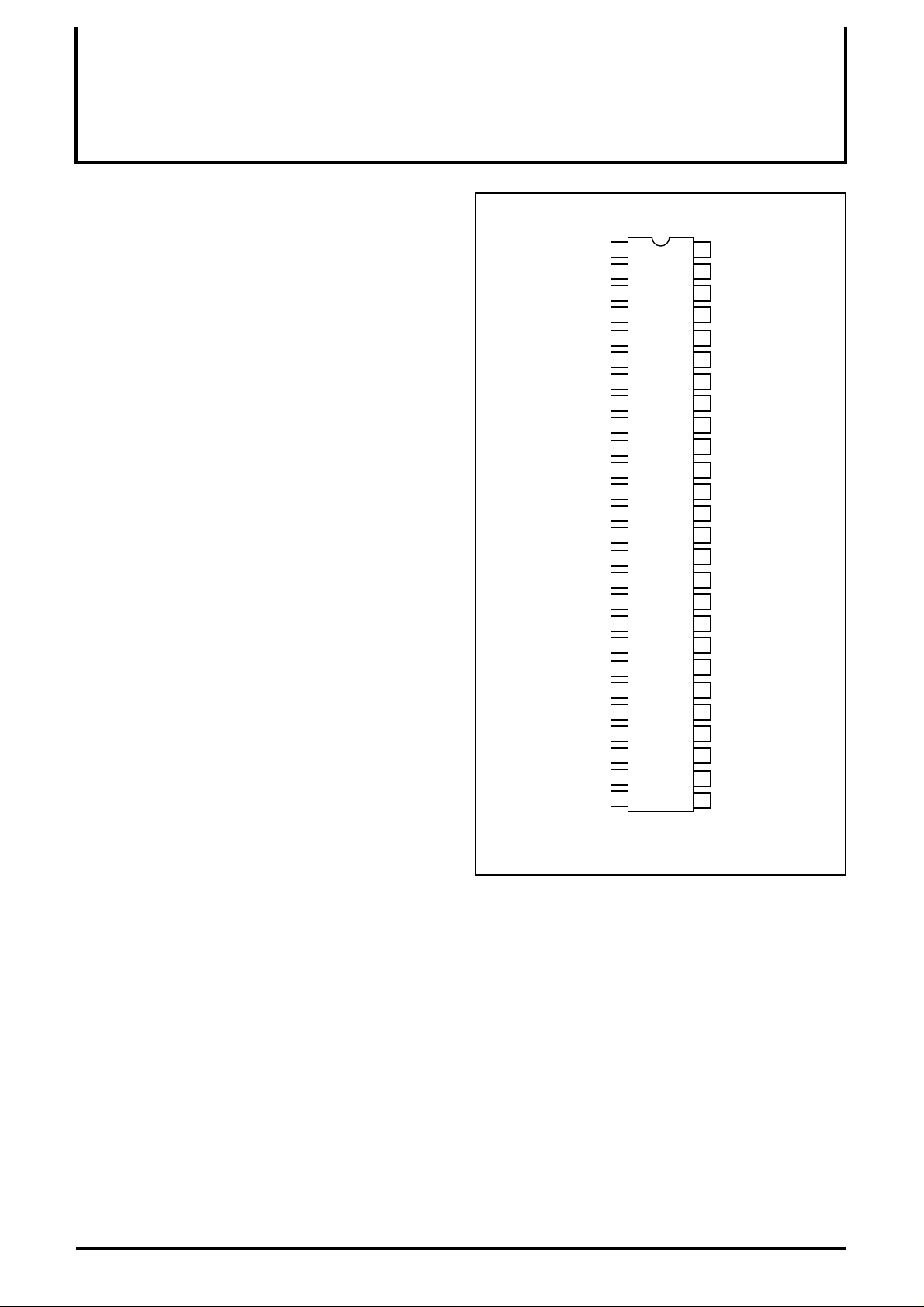
PIN CONFIGURATION (TOP VIEW)
AVss3 (vcxo)
VCXO out
VCXO in
FILTER
AVdd3 (vcxo)
AVdd2 (m)
Vin (m)
Vrt (m)
Vrb (m)
AVss2 (m)
AVdd1 (s)
Vrb (s)
AVss1 (s)
RESET
DVdd1
BGP(s)/TEST0
CSYNC(s)/TEST1
DVss2 (ram)
V
1
BIAS
Vin (s)
Vrt (s)
DVss1
SCK
ACK
DATA
CLK
1
2
3
4
5
6
7
8
9
10
11
12
13
14
15
16
17
18
19
20
21
22
23
24
25
26
Outline 52P4B
M65667SP
52
AVssf (ana)
51
Cin
50
TESTEN
49
Yin
TEST9
48
Y-PIP
47
TEST8
46
45
C-PIP
44
AVdd4 (da)
43
C-PIPin
AVss4 (da)
42
M65667SP
41
Y-PIPin
40
ADJ-Ysub
39
Yout-sub
38
ADJ-Csub
37
Cout-sub
36
DVss3
35
DVdd3
34
LOCK/TEST7
33
VD/CSYNC/TEST6
HD/TEST5
32
31
SWM/TEST4
30
MCK
29
fsc/TEST3
BGP(m)/TEST2
28
DVdd2 (ram)
27
NOTICE: Connect a 0.1 µ F or larger capacitor between V
pins.
1 : Include pin capacitance (7pF)
DD
and V
SS
1

MITSUBISHI ICs (TV)
PRELIMINARY
Notice:This is not a final specification.
Some parametric limits are subject to change.
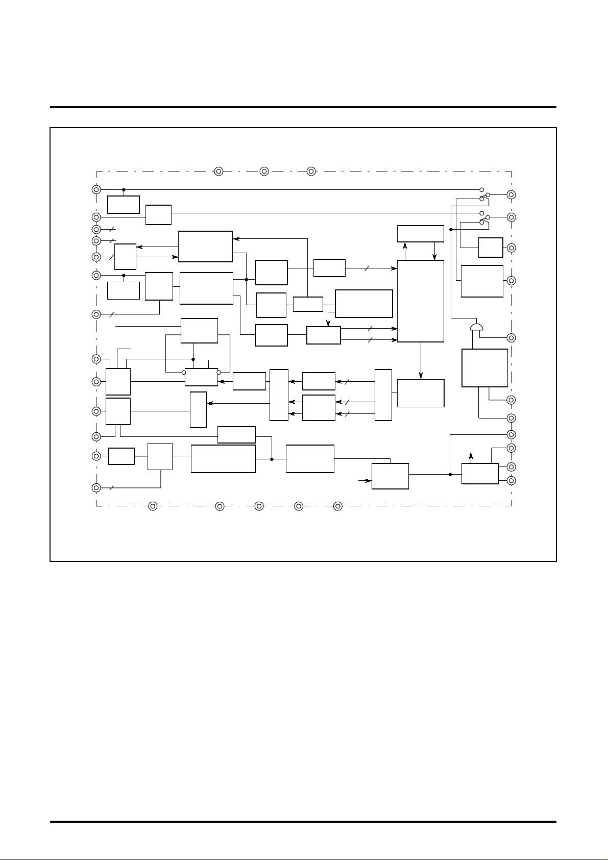
BLOCK DIAGRAM
Yin
Sync tip
Cin
Vdd / Vss
for test
DATA
CLK
ACK
Vin(s)
Vrt(m)
Vrb(m)
ADJ-Ysub
Yout-sub
Cout-sub
ADJ-Csub
Vin(m)
Vrt(m)
Vrb(m)
15
3
3
2
HD
2
Clamp
Sync tip
Clamp
D/A
8bit
D/A
8bit
Bias
I2C
I/F
Bias
A/D
8bit
2
C )
( I
A/D
8bit
HPLL
SCK
V-chip
data slicer
Y/C SEP
(LPF,BPF)
Phase
Select
4fsc
Delay
fsc
Encode
Burst Data
Sampling
Y
Level
Detect
CSYNC(s)
/TEST1
C
Delay
Luma
Clamp
Sync
Sep
Demod
MIX
M65667SP
PICTURE-IN-PICTURE SIGNAL PROCESSING
BGP(s)
/TEST0
RAM(1H)
Bias
C
Y6
Timing Gen
(Decode)
B-Y
R-Y
6Y
B-Y
6
R-Y
6
6
6
Demux
VCXO
Driver
Vert-filter
&
MUX
Y
B-Y
R-Y
RAM
96Kbits
Back Porch
Clamp
Timing Gen
(Memory
Cont)
4fsc
VCXO
Delay
AFC
Tint
Delay
LPF
&MPY
Phase
Detect
Lock/Free-run
via I
2
Y- PIP
C- PIP
C- PIPin
Y- PIPin
SWMG
/TEST7
VD
/CSYNC
/TEST6
HD
/TEST5
FILTER
BIAS
VCXO in
VCXO out
RESET
MCK
BGP(m)
/TEST2
fsc
/TEST3
SWM
/TEST4
2

MITSUBISHI ICs (TV)
PRELIMINARY
Notice:This is not a final specification.
Some parametric limits are subject to change.
PICTURE-IN-PICTURE SIGNAL PROCESSING
M65667SP
DESCRIPTION OF PIN
Pin No. Name I/O Function Remarks
1 AVss3
(VCXO)
2 VCXO out O VCXO output signal
3 VCXO in I VCXO input signal
4 FILTER I Filter
5 BIAS O Bias
6 AVdd3
(VCXO)
7 AVdd2 (m) Vdd Connect to analog power supply
8 Vin (m) I Chroma signal input (main-picture)
9 Vrt (m) O A/D Vref+ (main-picture)
10 Vrb (m) O A/D Vref- (main-picture)
11 AVss2 (m) GND Connect to analog GND
12 AVdd1 (s) Vdd Connect to analog power supply
13 Vin (s) I Composite video signal input (sub-picture)
14 Vrt (s) O A/D Vref+ (sub-picture)
15 Vrb (s) O A/D Vref- (sub-picture)
16 AVss1 (s) GND Connect to analog GND
17 RESET I Power on reset input signal ("L" reset)
18 DVss1 GND Connect to digital GND
19 DVdd1 Vdd Connect to digital power supply
20
BGP(s)/TEST0
21 SCK I For test (connect to digital GND) connect to GND
CSYNC(s)/TEST1
22
23 ACK O
24 DATA I
25 CLK I
26 DVss2(ram) GND Connect to digital GND
27 DVdd2(ram) Vdd Connect to digital power supply
BGP(m)/TEST2
28
29 fsc/TEST3 I(/O) For test (pull down to digital GND by resistor 15k Ω ) pull down 15k Ω
30 MCK I For test (connect to digital GND) connect to GND
31 SWM/TEST4 (I/)O For test non connect
32 HD/TEST5 I(/O) Horizontal sync input signal (Positive going edge is used)
VD/CSYNC
33
/TEST6
SWMG/TEST7
34
35 DVdd3 Vdd Connect to digital power supply
36 DVss3 GND Connect to digital GND
37 Cout-sub O D/A output signal (Chroma signal of sub-picture)
38 ADJ-Csub I D/A adjust for chroma signal (sub-picture)
39 Yout-sub O D/A output signal (Luma signal of sub-picture)
40 ADJ-Ysub I D/A adjust for luma signal (sub-picture)
41 Y-PIPin I PIP luma signal re-input
42 AVss4 (da) GND Connects to analog GND
43 C-PIPin I PIP chroma signal re-input
44 AVdd4 (da) Vdd Connect to analog power supply
45 C-PIP O PIP chroma signal output
46 TEST8 I For test (connect to analog GND) pull up 15k Ω
47 Y-PIP O PIP luma signal output
48 TEST9 I For test (connect to analog GND) connect to GND
49 Yin I Luma input signal (main-picture)
50 TESTEN I For test (connect to analog GND) connect to GND
51 Cin I Chroma input signal (main-picture)
52 AVssf (ana) Vss Connect to analog GND
GND Connects to analog GND
Vdd Connect to analog power supply
100k Ω to V
(I/)O For test non connect
I(/O) For test (connect to digital GND) pull down 15k Ω
2
I
C bus-data/Acknowledge output signal
2
I
C bus-data input signal
2
I
C bus-clock input signal
(I/)O For test non connect
I(/O) Vertical sync input signal (active "H")
I(/O) Enable input signal to display sub picture ("H" enable) pull up 15k Ω
,10 µ F to GND
DD
3
 Loading...