×
×
∗
∗
MITSUBISHI ICs (TV)
PRELIMINARY
Notice:This is not a final specification.
Some parametric limits are subject to change.
DESCRIPTION
The M65667FP is a NTSC PIP (Picture in Picture) signal
processing LSI, whose sub and main-picture inputs are composite
and Y/C separated signals, respectively. The built-in field memory
(96k-bit RAM) ,V-chip data slicer and analog circuitries lead the PIP
system low cost and small size.
FEATURES
•
Built-in 96k-bit field memory (sub-picture data storage)
•
Internal V-chip data slicer (for sub-picture)
•
Vertical filter for sub-picture (Y signal )
•
Single sub-picture (selectable picture size : 1/9 , 1/16)
•
Sub-picture processing sepecification (1/9 size / 1/16 size) :
Quantization bits Y, B-Y, R-Y : 6bits
Horizontal sampling 171 pixels (Y) , 28.5 pixels (B-Y, R-Y)
Vertical lines 69/ 52 lines
•
Frame (sub-picture) on/off
•
Built-in analog circuits :
Two 8-bit A/D converters (main and sub-picture signals)
Two 8-bit D/A converters (Y and C sub-picture signals)
Sync-tip-clump, VCXO, Analog switch ... etc.
2
I
C BUS control (parallel/serial control) :
•
PIP on/off , Sub-picture size(1/9 or 1/16), Frame on/off
(programmable luma level), PIP position (4 corners fixed
position), Picture freeze , Y delay adjustment, Chroma level, Tint,
Black level, Contrast ... etc.
M65667FP
PICTURE-IN-PICTURE SIGNAL PROCESSING
APPLICATION
NTSC color TV
RECOMMENDED OPERATING CONDITION
Supply voltage range........................................................3.1 to 3.5V
Operating frequency.........................................................14.32 MHz
Operating temperature....................................................-20 to 75 ° C
Input voltage (CMOS interface)"H"........................V
"L".............................0 to V
Output current (output buffer)........................................ ± 4mA (MAX)
Output load capacitance............................................20pF (MAX)
Circuit current.........................................................................160mA
NOTICE: Connect a 0.1 µ F or larger capacitor between V
pins.
1 : Include pin capacitance (7pF)
DD
0.7 to V
DD
DD
and V
DD
0.3V
SS
V
1
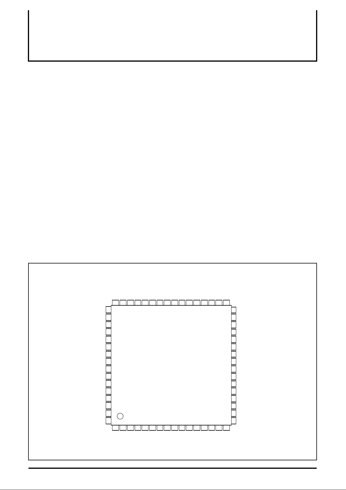
PIN CONFIGURATION (TOP VIEW)
C-PIP
48
NC
49
50
TEST8
51
Y-PIP
TEST9
52
53
Yin
Cin
(VCXO)
FILTER
BIAS
(VCXO)
54
55
56
57
58
59
60
61
62
63
64
1
Vin (m)
TESTEN
AVss (ana)
AVss3
VCXO out
VCXO in
AVdd3
AVdd2 (m)
AVdd2 (m)
AVdd4 (da)
47
2
Vrt (m)
AVdd4 (da)
AVdd4 (da)
46
454443
3
4
Vrb (m)
AVss2 (m)
(da)
C-PIPin
AVss4
AVss4 (da)
42
M65667FP
5
6
7
AVdd1 (s)
AVdd1 (s)
AVss2 (m)
Outline 64P6N-A
Y-PIPin
ADJ-Ysub
41
403938
8
9
Vrt (s)
Vin (s)
Yout-sub
ADJ-Csub
101112
Vrb (s)
AVss1 (s)
Cout-sub
DVss3
37
363534
131415
RESET
AVss1 (s)
DVdd3
LOCK/TEST7
DVss1
DVdd1
NC
33
NC
32
VD/CSYNC/TEST6
31
HD/TEST5
30
29
SWM/TEST4
MCK
28
27
fsc/TEST3
26
BGP (m)/TEST2
25
DVdd2 (ram)
DVss2 (ram)
24
23
CLK
22
DATA
21
ACK
20
CSYNC (s)/TEST1
19
SCK
18
BGP (s)/TEST0
17
NC
16
NC
NC : NO CONNECTION
1

MITSUBISHI ICs (TV)
PRELIMINARY
Notice:This is not a final specification.
Some parametric limits are subject to change.
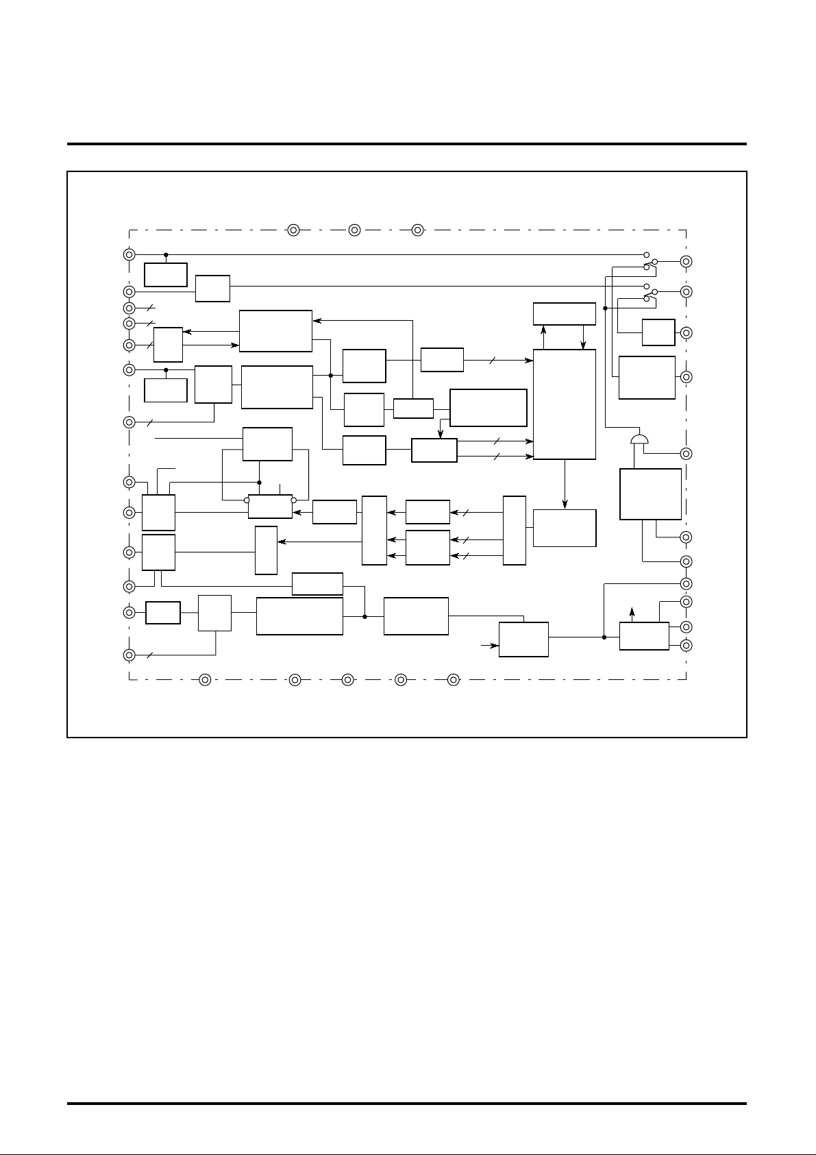
BLOCK DIAGRAM
Yin
Sync tip
Cin
Vdd / Vss
for test
DATA
CLK
ACK
Vin(s)
Vrt(m)
Vrb(m)
ADJ-Ysub
Yout-sub
Cout-sub
ADJ-Csub
Vin(m)
Vrt(m)
Vrb(m)
15
3
3
2
HD
2
Clamp
Sync tip
Clamp
D/A
8bit
D/A
8bit
Bias
I2C
I/F
Bias
A/D
8bit
2
C )
( I
A/D
8bit
HPLL
SCK
V-chip
data slicer
Y/C SEP
(LPF,BPF)
Phase
Select
4fsc
Delay
fsc
Encode
Burst Data
Sampling
Y
Level
Detect
CSYNC(s)
/TEST1
C
Delay
Luma
Clamp
Sync
Sep
Demod
MIX
M65667FP
PICTURE-IN-PICTURE SIGNAL PROCESSING
BGP(s)
/TEST0
RAM(1H)
Bias
C
Y6
Timing Gen
(Decode)
B-Y
R-Y
6Y
B-Y
6
R-Y
6
6
6
VCXO
Driver
Demux
Vert-filter
&
MUX
Y
B-Y
R-Y
RAM
96Kbits
Back Porch
Clamp
Timing Gen
(Memory
Cont)
4fsc
VCXO
Delay
AFC
Tint
Delay
LPF
&MPY
Phase
Detect
Lock/Free-run
via I
2
Y- PIP
C- PIP
C- PIPin
Y- PIPin
SWMG
/TEST7
VD
/CSYNC
/TEST6
HD
/TEST5
FILTER
BIAS
VCXO in
VCXO out
RESET
MCK
BGP(m)
/TEST2
fsc
/TEST3
SWM
/TEST4
2

MITSUBISHI ICs (TV)
PRELIMINARY
Notice:This is not a final specification.
Some parametric limits are subject to change.
PICTURE-IN-PICTURE SIGNAL PROCESSING
M65667FP
DESCRIPTION OF PIN
Pin No. Name I/O Function Remarks
1 Vin (m) I Chroma signal input (main-picture)
2 Vrt (m) O A/D Vref+ (main-picture)
3 Vrb (m) O A/D Vref- (main-picture)
4 AVss2 (m) GND Connect to analog GND
5 AVss2 (m) GND Connect to analog GND
6 AVdd1 (s) Vdd Connect to analog power supply
7 AVdd1 (s) Vdd Connect to analog power supply
8 Vin (s) I Composite video signal input (sub-picture)
9 Vrt (s) O A/D Vref+ (sub-picture)
10 Vrb (s) O A/D Vref- (sub-picture)
11 AVss1 (s) GND Connect to analog GND
12 AVss1 (s) GND Connect to analog GND
13 RESET I Power on reset input signal ("L" reset)
14 DVss1 GND Connect to digital GND
15 DVdd1 Vdd Connect to digital power supply
16 NC
17 NC
18
BGP(s)/TEST0
(I/)O For test non connect
19 SCK I For test (connect to digital GND) connect to GND
20
21 ACK O
22 DATA I
23 CLK I
CSYNC(s)/TEST1
I(/O) For test (connect to digital GND) pull down 15k Ω
2
I
C bus-data/Acknowledge output signal
2
I
C bus-data input signal
2
I
C bus-clock input signal
24 DVss2(ram) GND Connect to digital GND
25 DVdd2(ram) Vdd Connect to digital power supply
26
BGP(m)/TEST2
(I/)O For test non connect
27 fsc/TEST3 I(/O) For test (pull down to digital GND by resistor 15k Ω ) pull down 15k Ω
28 MCK I For test (connect to digital GND) connect to GND
29 SWM/TEST4 (I/)O For test non connect
30 HD/TEST5 I(/O) Horizontal sync input signal (Positive going edge is used)
31
VD/CSYNC
/TEST6
I(/O) Vertical sync input signal (active "H")
32 NC
33 NC
34
SWMG/TEST7
I(/O) Enable input signal to display sub picture ("H" enable) pull up 15k Ω
35 DVdd3 Vdd Connect to digital power supply
36 DVss3 GND Connect to digital GND
37 Cout-sub O D/A output signal (Chroma signal of sub-picture)
38 ADJ-Csub I D/A adjust for chroma signal (sub-picture)
39 Yout-sub O D/A output signal (Luma signal of sub-picture)
40 ADJ-Ysub I D/A adjust for luma signal (sub-picture)
41 Y-PIPin I PIP luma signal re-input
42 AVss4 (da) GND Connects to analog GND
43 AVss4 (da) GND Connects to analog GND
44 C-PIPin I PIP chroma signal re-input
45 AVdd4 (da) Vdd Connect to analog power supply
46 AVdd4 (da) Vdd Connect to analog power supply
47 AVdd4 (da) Vdd Connect to analog power supply
48 C-PIP O PIP chroma signal output
49 NC
50 TEST8 I For test (connect to analog GND) pull up 15k Ω
51 Y-PIP O PIP luma signal output
52 TEST9 I For test (connect to analog GND) connect to GND
100k Ω to V
,10 µ F to GND
DD
3
 Loading...