×
×
∗
∗
MITSUBISHI ICs (TV)
M65617SP
PICTURE-IN-PICTURE SIGNAL PROCESSING
DESCRIPTION
This system is an NTSC system PinP system that accommodates
subscreen composite input and main screen Y/C input. It is a
semiconductor IC circuit having a built-in 96K bit field memory and
an analog circuit, which permits a low-cost and compact system
configuration.
FEATURES
•
Built-in field memory 96K bit for PIP
•
Built-in luminance signal vertical filter
•
No. of subscreen displays: 1 (two sizes, 1/9 and 1/16, can be
selected from.)
•
No. of subscreen samples (1/9 - 1/16 sizes)
No. of quantization bits: 6 for all Y, B-Y and R-Y
No. of horizontal picture elements: 171(Y), 28.5 (B-Y, R-Y)
No. of vertical lines: 69/52
Subscreen frame display ON/OFF
•
Built-in analog circuits such as sync chip clamp, VCXO, and ana-
•
log switch
Built-in 2 channels of 8 bit A/D converter
•
(for main signal burst lock and PIP sub signal)
Built-in two channels of 8 bit D/A converter (luminance and
•
chroma signals)
2
•
I
C bus control
Controls: display ON/OFF, display size selection, setting of
display position, frame ON/OFF, setting of frame level, selection
of frame animation/field still image, setting of Y delay amount,
color level, tint, black level, etc.
APPLICATION
TV
RECOMMENDED OPERATING CONDITION
Supply voltage range........................................................3.1 to 3.5V
Operating frequency.........................................................14.32 MHz
Operating temperature....................................................-10 to 75 ° C
Input voltage (CMOS interface)"H"........................V
DD
"L".............................0 to V
Output current (output buffer)........................................ ± 4mA (MAX)
Output load capacitance............................................20pF (MAX)
Circuit current.........................................................................140mA
0.7 to V
DD
DD
0.3V
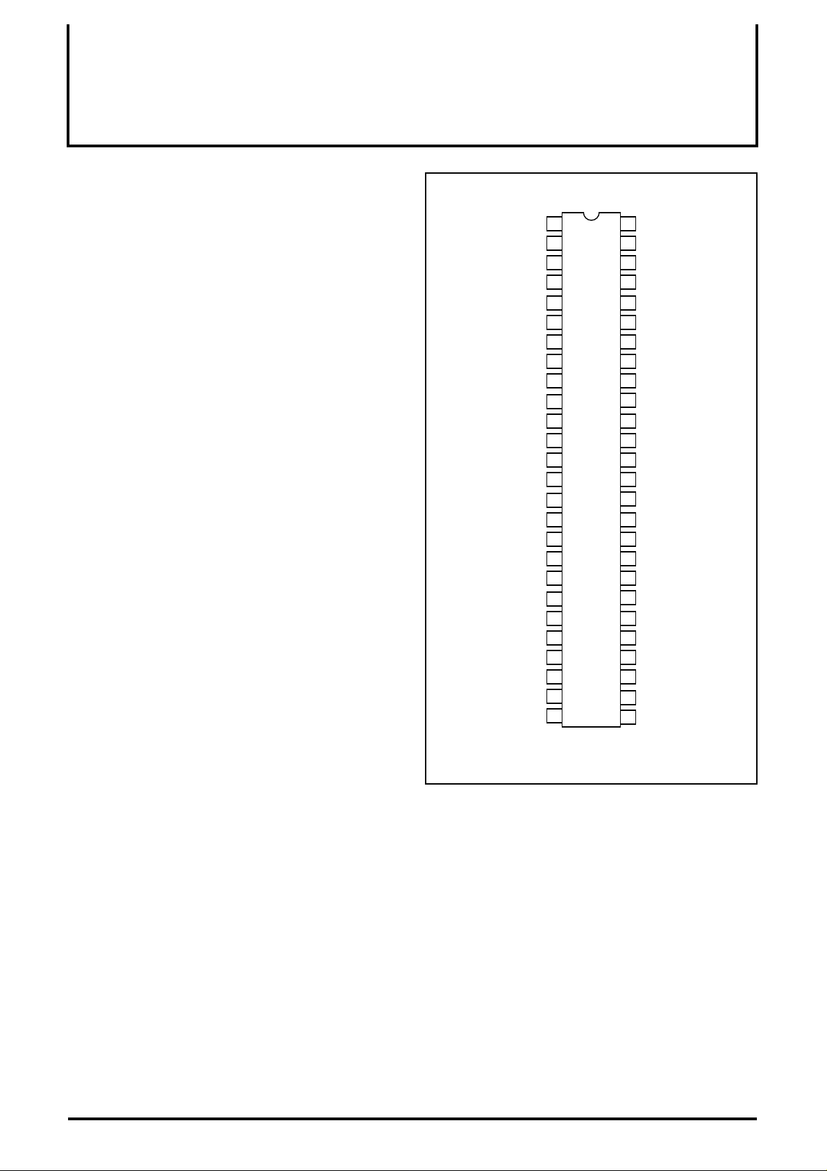
PIN CONFIGURATION (TOP VIEW)
AVss3 (vcxo)
VCXO out
VCXO in
FILTER
AVdd3 (vcxo)
AVdd2 (m)
Vin (m)
Vrt (m)
Vrb (m)
AVss2 (m)
AVdd1 (s)
Vrb (s)
AVss1 (s)
RESET
DVdd1
BGP(s)/TEST0
CSYNC(s)/TEST1
V
1
BIAS
Vin (s)
Vrt (s)
DVss1
SCK
ACK
DATA
CLK
DVss2
1
2
3
4
5
6
7
8
9
10
11
12
13
14
15
16
17
18
19
20
21
22
23
24
25
26
Outline 52P4B
52
51
50
49
48
47
46
45
44
43
42
M65617SP
41
40
39
38
37
36
35
34
33
32
31
30
29
28
27
AVssf (ana)
Cin
TESTEN
Yin
TEST9
Y-PIP
TEST8
C-PIP
AVdd4 (da)
C-PIPin
AVss4 (da)
Y-PIPin
ADJ-Ysub
Yout-sub
ADJ-Csub
Cout-sub
DVss3 (ram)
DVdd3 (ram)
SWMG/TEST7
VD/CSYNC/TEST6
HD/TEST5
SWM/TEST4
MCK
fsc/TEST3
BGP(m)/TEST2
DVdd2
NOTICE: Connect a 0.1 µ F or larger capacitor between V
pins.
1 : Include pin capacitance (7pF)
1
DD
and V
SS

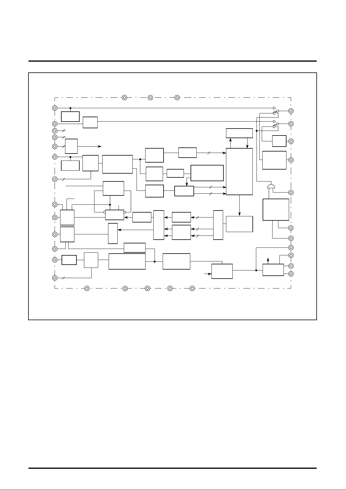
BLOCK DIAGRAM
MITSUBISHI ICs (TV)
M65617SP
PICTURE-IN-PICTURE SIGNAL PROCESSING
SCK
CSYNC(s)
/TEST1
BGP(s)
/TEST0
Yin
Cin
Vdd / Vss
for test
DATA
CLK
ACK
Vin(s)
Vrt(m)
Vrb(m)
ADJ-Ysub
Yout-sub
Cout-sub
ADJ-Csub
Vin(m)
Vrt(m)
Vrb(m)
15
3
3
2
HD
2
Sync tip
Clamp
I2C
I/F
Sync tip
Clamp
D/A
8bit
D/A
8bit
Bias
Y- PIP
Bias
RAM(1H)
Bias
C
Y6
Timing Gen
(Decode)
B-Y
R-Y
6Y
B-Y
6
R-Y
6
6
6
Demux
VCXO
Driver
Vert-filter
&
MUX
Y
B-Y
R-Y
RAM
96Kbits
Back Porch
Clamp
Timing Gen
(Memory
Cont)
4fsc
VCXO
Luma
Y
C
Delay
Clamp
Sync
Sep
Demod
MIX
A/D
8bit
2
C )
( I
A/D
8bit
HPLL
Y/C SEP
(LPF,BPF)
Phase
Select
4fsc
Delay
fsc
Encode
Burst Data
Sampling
Level
Detect
Delay
AFC
Tint
Delay
LPF
&MPY
Phase
Detect
Lock/Free-run
via I
2
C- PIP
C- PIPin
Y- PIPin
SWMG
/TEST7
VD
/CSYNC
/TEST6
HD
/TEST5
FILTER
BIAS
VCXO in
VCXO out
RESET
MCK
BGP(m)
/TEST2
fsc
/TEST3
SWM
/TEST4
2

MITSUBISHI ICs (TV)
M65617SP
PICTURE-IN-PICTURE SIGNAL PROCESSING
DESCRIPTION OF PIN
Pin No. Name I/O Function Remarks
1 AVss3
(VCXO)
2 VCXO out O Oscillation output signal
3 VCXO in I Oscillation input signal
4 FILTER O Filter
5 BIAS O Bias
6 AVdd3
(VCXO)
7 AVdd2 (m) Vdd Power supply (analog main signal A/D section)
8 Vin (m) I Main color input signal
9 Vrt (m) O Main signal A/D reference voltage output +
10 Vrb (m) O Main signal A/D reference voltage output 11 AVss2 (m) GND Grounding (analog main signal A/D section)
12 AVdd1 (s) Vdd Power supply (analog sub-signal A/D section)
13 Vin (s) I Sub-composite video input signal
14 Vrt (s) O Sub-signal A/D reference voltage output +
15 Vrb (s) O Sub-signal A/D reference voltage output 16 AVss1 (s) GND Grounding (analog sub-signal A/D section)
17 RESET I Power-ON reset input signal.
18 DVss1 GND Grounding (digital section)
19 DVdd1 Vdd Power supply (digital section)
BGP(s)/TEST0
20
21 SCK I Sub-screen 4fsc clock input Grounding
CSYNC(s)/TEST1
22
23 ACK O
24 DATA I
25 CLK I
26 DVss2 GND Grounding (digital section)
27 DVdd2 Vdd Power supply (digital section)
BGP(m)/TEST2
28
29 fsc/TEST3 I(/O) For testing Pulldown 15k Ω
30 MCK I For testing Grounding
31 SWM/TEST4 (I/)O For testing Open
32 HD/TEST5 I(/O) Horizontal sync input signal
VD/CSYNC/
33
TEST6
SWMG/TEST7
34
35 DVdd3 (ram) Vdd Power supply (digital RAM section)
36 DVss3 (ram) GND Grounding (digital RAM section)
37 Cout-sub O Sub-screen color signal D/A output signal
38 ADJ-Csub O For adjustment of sub-screen color signal D/A
39 Yout-sub O Sub-screen luminance signal D/A output signal
40 ADJ-Ysub O For adjustment of sub-screen luminance signal D/A
41 Y-PIPin I Sub-screen luminance signal re-input signal
42 AVss4 (da) GND Grounding (analog D/A and SW sections)
43 C-PIPin I Sub-screen color signal re-input signal
44 AVdd4 (da) Vdd Power supply (analog D/A & SW sections)
45 C-PIP O PIP color signal output signal
46 TEST8 I For testing Pullup 15k Ω
47 Y-PIP O PIP luminance signal output signal
48 TEST9 I For testing Grounding
49 Yin I Main luminance input signal
50 TESTEN I For testing Grounding
51 Cin I Main color input signal
52 AVssf (ana) Vss Grounding (analog section)
GND Grounding (analog burst lock PLL section)
Vdd Power supply (analog burst lock PLL section)
Connected to the power supply with
100k Ω , and grounded with 10 µ F
(I/)O Sub-screen burst gate pulse output Open
I(/O) Sub-screen CSYNC input Pulldown 15k Ω
2
I
C bus data/acknowledge output signal
2
I
C bus data input signal
2
I
C bus clock input signal
(I/)O For testing Open
I(/O) Vertical sync input signal
I(/O) Sub-screen display authorization input signal Pullup 15k Ω
3

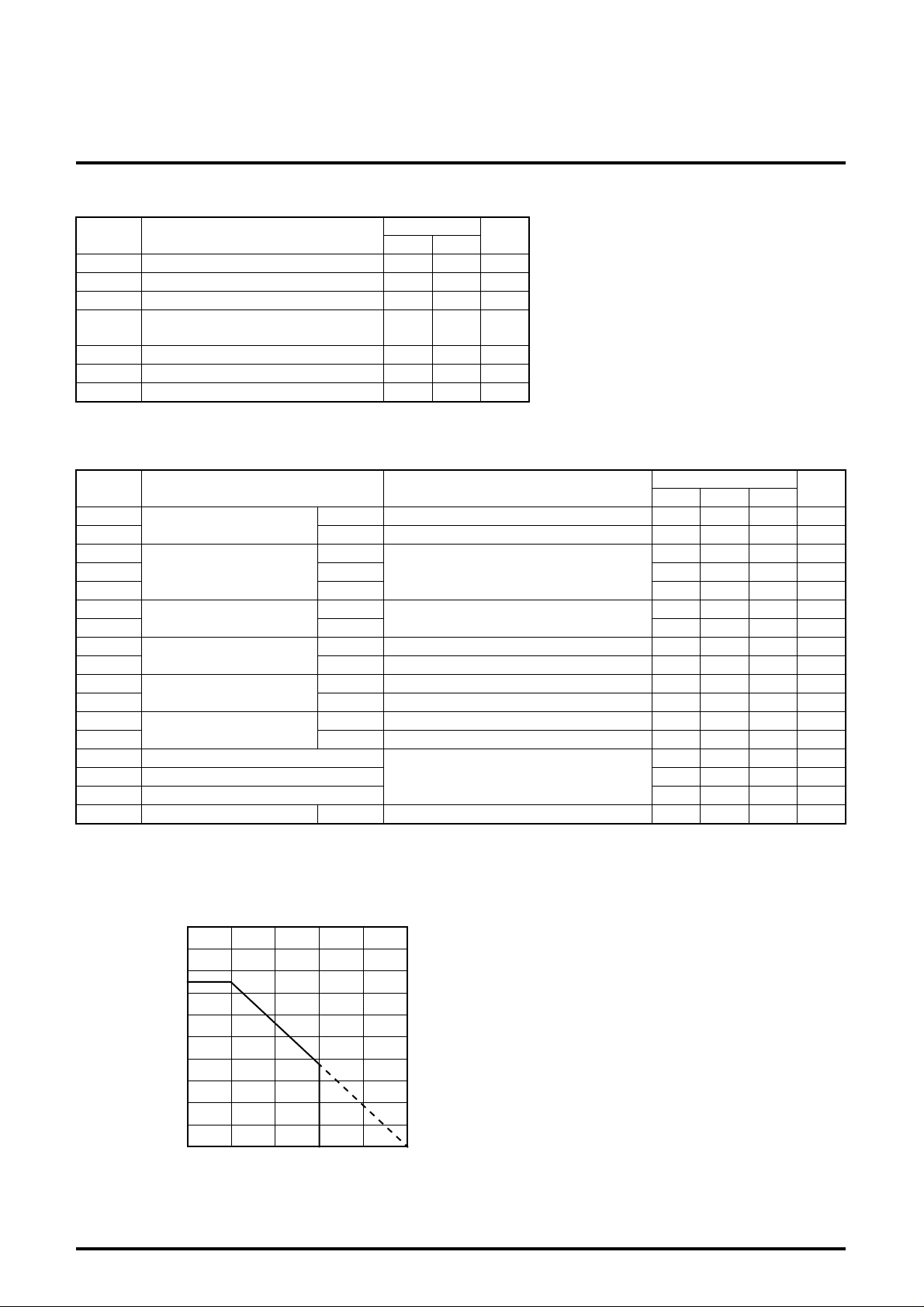
ABSOLUTE MAXIMUM RATINGS
Symbol Parameter
V
DD3
V
I
V
O
O
I
P
d
T
opr
T
stg
1: Output current per output terminal. But P
Supply voltage (3.3V) -0.3 4.6 V
Input voltage -0.3
Output voltage -0.3
Output current
1)
Power dissipation
Operating temperature -10 75 ° C
Storage temperature -50 125 ° C
d
limits all current.
(V
SS
=0V)
∗
Limits
Min. Max.
−
−
V
+0.3
DD3
V
+0.3
DD3
OL
I
=20
I
OH
=-26
1400 mW
( ∗
−
−
−
−
−
−
|
−
MITSUBISHI ICs (TV)
M65617SP
PICTURE-IN-PICTURE SIGNAL PROCESSING
Unit
V
V
mA
−
−
−
−
−
−
SS
(V
DC ELECTRICAL CHARACTERISTICS
=0V)
Symbol Parameter Test conditions
V
IL
V
IH
V
T
-
V
T
+ + 1.4
V
H
V
OL
V
OH
I
OL
I
OH
I
IH
I
IL
I
OZL
I
OZH
C
I
C
O
C
IO
I
DD
Input voltage
(CMOS interface)
Input voltage schmitt trigger
(CMOS interface)
Output voltage
Output current
Input current
Output leakage current
Input pin capacitance
Output pin capacitance
Bidirectional pin capacitance
Operating current
L level V
H level V
DD
=2.7V 0
DD
=3.6V 2.52
–
DD
=3.3V
V
Hysteresis
L level
H level 3.25
L level V
H level V
L level V
H level V
L level V
H level V
3.3V supply
V
DD
=3.3V, | I
DD
=3.0V , V
DD
=3.0V , V
DD
=3.6V , V
DD
=3.6V , V
DD
=3.6V , V
DD
=3.6V , V
f=1MHz, V
O
<1 µ A
OL
=0.4V 4
OH
=2.6V
I
=0V -1
I
=3.6V -1
O
=0V -1
O
=3.6V -1
DD
=0V
TYPICAL CHARACTERISTICS
Limits
Min. Typ. Max.
0.81 V
3.6 V
0.5
1.65 V
2.4 V
0.3
−−
1.2 V
0.05 V
−−
−−
−−
-4 mA
1 µ A
1 µ A
1 µ A
1 µ A
7 15 pF
7 15 pF
7 15 pF
−− 140 mA
Unit
V
mA
THERMAL DERATING (MAXIMUM RATING)
2000
1600
1490
1200
800
400
POWER DISSIPATION Pd (mW)
0
0 25 75 125
50
100
AMBIENT TEMPERATURE Ta (°C)
4

PICTURE-IN-PICTURE SIGNAL PROCESSING
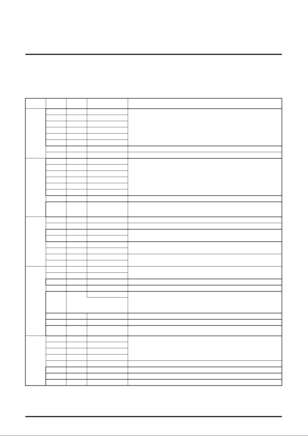
SERIAL REGISTER INFORMATION (device address=24h, sub-address=00h to 0Fh)
Registers requiring user selection/adjustment setting are enclosed in rectangles.
Indication method of reference setting column:Thick letters: Fixed setting value
Standard letters: An example as setting for evaluation
∗/∗: 1/9 - 1/16 sizes
Sub-
address
00h
01h
02h
03h
04h
Bit No.
Reference
setting
0 1 color (0)
1 1 color (1)
2 1 color (2)
3 1 color (3)
4 1 color (4)
5 1 color (5)
6 1 color (6) [1 setting]
7 0 killer Color killer; ON [0], OFF [1], [0 setting]
0 0 tint (0)
1 0 tint (1)
2 0 tint (2)
3 0 tint (3)
4 0 tint (4)
5 0 tint (5)
6 0 afcoff [0 setting]
7 NB decode
0 0 evenupra Setting of interlace leading line; leading field first/second [1/0], [0 setting]
1 0 bgcs Forced writing of background level [1 significant, normally 0] [0 setting]
2 0 extport (0)
3 1 extport (1)
4 0 adclocksel (0)
5 0 adclocksel (1)
6 1 mode (0)
7 0 mode (1)
0 1 crtint (0)
1 1 crtint (1)
2 1/0 size-h Horizontal size
3 0 hpfoff Emphasis of high luminance signal area ON/OFF [0/1] [0 setting]
NB bgpmsel
1 in case of 03h<7>(rvs)=1 or
4
03h<6>(rvhs)=1,
0 in other cases
5 0/1 size Vertical size
6 0 rvhs Addition of sync, burst; OFF/ON [0/1] [Normally 0 setting when PIP is displayed]
70rvs
0 0 ydl (0)
1 0 ydl (1)
2 1 ydl (2)
3 0 ydl (3)
4 0 test acc lvl acc reference level setting authorization; [1 significant] [0 setting]
5 1 wen Display of field still screen/display of animation [0/1]
6 1 grc Display of sub-screen frame; NO/YES [0/1]
7 NB stnby=testreset [0] setting (memory access not operated by [1])
Register name Function
Color saturation adjustment; min. value [0], max. value[63], 1/step [3Fh setting]
Tint adjustment; setting by complements of 2
0fl to -50fl [00h to 1Fh]
+50fl to 0fl [20h to 3Fh]
[Normally 00h setting]
Initialization of sub-screen color demodulation; normally [0], initialized [1]
Each time reset is cleared and sub-screen input source changed, operate in a
sequence of 0 - 1 - 0.
2
C bus expansion port data (optional function); [Set to either of them]
I
Selection of adc clock delay; [00b setting]
Selection of IC operation mode; [01b setting] 16 bits [0]
Setting of sub-screen tint offset; [11b setting]
Selection of PIP-Y output clamping pulse; [0 setting when PIP is displayed]
Sync operation; Main input is f ollo w ed [0], self-propelled [1] [0 setting when PIP is
displayed]
Setting of sub-screen Y delay amount
(D/A output phase against color signal); [4 setting]
Min. 280ns [0h], center 0ns [4h], max. +770ns [Fh]
MITSUBISHI ICs (TV)
M65617SP
5
 Loading...