

MITSUBISHI ICs (TV)
M64897GP
PLL FREQUENCY SYNTHESIZER WITH DC-DC CONVERTER FOR PC
DESCRIPTION
The M64897GP is a semiconductor integrated circuit consisting of
PLL frequency synthesizer for TV/VCR/PC using I
2
C BUS control.
It contains the prescaler with operating up to1.3GHz, 4 band drivers
and DC-DC converter for Tuning voltage.
FEATURES
Built-in DC-DC converter for Tuning voltage
•
4 integrated PNP band drivers
•
(Io=30mA, Vsat=0.2V typ@Vcc1 to 10V)
Built-in prescaler with input amplifier (f max=1.3GHz)
•
PLL lock/unlock status display out put
•
(Built-in pull up resistor)
X’tal 4MHz is used to realize 3 type of tuning steps
•
(Divider ratio 1/512, 1/640, 1/1024)
•
Software compatible with M64894
•
Built-in Power on reset system
•
Small Package (SSOP)
APPLICATION
PC, TV, VCR tuners
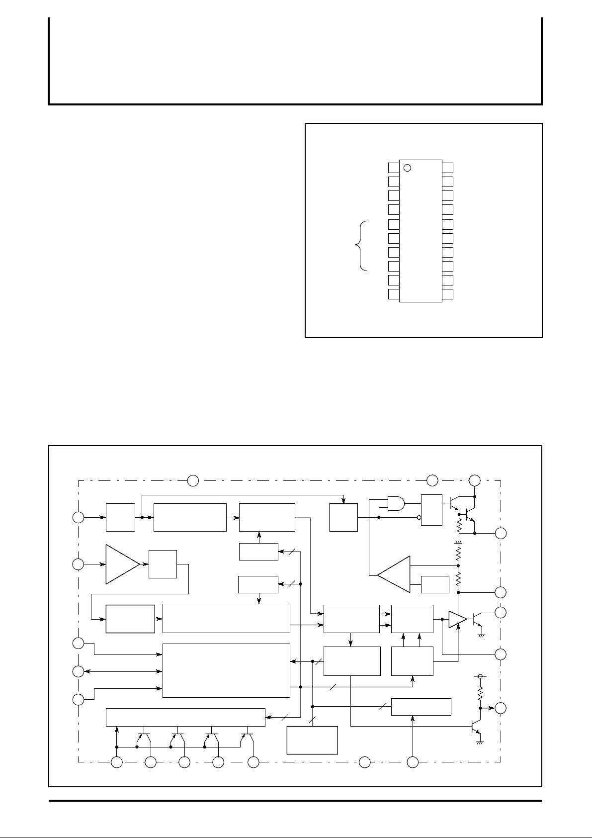
PIN CONFIGURATION (TOP VIEW)
PRESCALER
INPUT
GND
SUPPLY
VOLTAGE 1
SUPPLY
VOLTAGE 2
BAND
SWITCHING
OUTPUTS
DC-DCSUPPLY
VOLTAGE
PEACK CURRENT
DETECT
fin
GND
CC1
V
CC2
V
BS4
BS3
BS2
BS1
VDC
Ipk
1
2
3
4
20
19
18
M64897GP
17
165
156
147
138
129
1110
Xin
ADS
SDA
SCL
LD/ftest
ADC
Vin
Vtu
+B
SWE
CRYSTAL
OSCILLATOR
CHIP ADDRESS
INPUT
DATA INPUT
CLOCK INPUT
LD/ftest
OUTPUT
A/D INPUT
FILTER INPUT
TUNING
OUTPUT
SUPPLY
VOLTAGE
SWITCHING
OUTPUT
Outline 20P2E-A
RECOMMENDED OPERATING CONDITION
Supply voltage range..............................................V
Rated supply voltage...........................................................V
CC1
V
CC2
=4.5 to 5.5V
=V
CC1
V
to 10V
CC1
CC2
=V
=5V
CC1
BLOCK DIAGRAM
Xin
SCL
SDA
ADS
20
1
fin
17
18
19
OSC
AMP
1/32,1/33
CC1 VDC Ipk
V
3
f REF DIVIDER SELECTER
1/8
15bit
PROGRAMMABLE DIVIDER
BUS CONTROLLER
ADDRESS SELECT
BAIS / BAND SWITCH DRIVER
LATCH
LATCH
2
15
4
1
1
Power
On Reset
DIV.
PHASE
DETECTOR
LOCK
DETECTOR
5
-
+
CHARGE
PUMP
CP TEST
LATCH
3
5-LEVEL A/D
SRQ
Vreg
OS
109
11
SWE
12
+B
Vtu
13
14
Vin
16
LD/ftest
7654 2 15
8
GND ADCVCC2 BS4 BS3 BS2 BS1
1
°
°
PLL FREQUENCY SYNTHESIZER WITH DC-DC CONVERTER FOR PC
DESCRIPTION OF PIN
Pin No. Symbol Pin name Function
1 f in Prescaler input Input for the VCO frequency.
2 GND GND Ground to 0V.
3V
4V
CC1
CC2
5 BS4
6 BS3
7 BS2
8 BS1
9 VDC
10 Ipk
11 SWE Switching output DC-DC converter oscillator output.
12 +B
13 Vtu Tuning output This supplies the tuning voltage.
14
Vin
15 LD/ftest Lock detect /Test port
16 ADC AD converter input A/D conversion of the input voltage.
17 SCL Clock input Data is read into the shift register when the clock signal falls.
18
SDA Data input
19 ADS
20 X in
Power supply voltage 1
Power supply voltage 2
Band switching
outputs
DC-DC power
supply voltage
Peack current
detect
Power supply
voltage
Filter input
(Charge pump output)
Address switching input
This is connected to
the crystal oscillator
Power supply voltage terminal. 5.0V ± 0.5V
Power supply for band switching, Vcc
1
to 10V
PNP open collector method is used.
When the band switching data is "H", the output is ON.
When it is "L", the output is OFF.
DC-DC power supply voltage terminal. 5.0V ± 0.5V
When potential difference with VDC terminal becomes more than 0.33V by current
limiting detector of DC-DC converter, the listing rises with off.
Power supply voltage for turning voltage.
This is the output terminal for the LPF input and charge pump output. When the phase
of the programmable divider output (f 1/N) is ahead compared to the reference
frequency (f
), the "source" current state becomes active.
REF
If it is behind, the "sink" current becomes active.
If the phases are the same, the high impedance state becomes active.
Lock detector output. When loop of phase locked loop locked it, it rises with "H" level
in "L" level or unlock.
In control byte data input, the programmabule freq. divider output and reference freq.
output is selected by the test mode.
Input for band SW and programmable freq. divider set up.
In lead mode, itoutputs lock detector output and power down flag and a state of 5 le v el
A/D converter.
Chip address sets it up with the input condition of terminal.
4.0MHz crystal oscillator is connected.
MITSUBISHI ICs (TV)
M64897GP
ABSOLUTE MAXIMUM RATINGS
(Ta=-20 ° C to +75 ° C, unless otherwise noted)
Symbol Parameter Conditions Ratings Unit
V
CC1
V
CC2
V
I
V
O
BSOFF
V
I
BSON
BSON
t
d
P
opr
T
stg
T
Supply voltage 1 Pin3 6.0 V
Supply voltage 2 Pin4 10.8 V
Input voltage Not to exceed Vcc
Output voltage f
REF
output 6.0 V
Voltage applied when
the band output is OFF
1
6.0 V
10.8 V
Band output current per 1 band output circuit 40.0 mA
ON the time when the
band output is ON
40mA per 1 band output circuit
3circuits are pn at same time,
10 sec
Power dissipation Ta=75 ° C 255 mW
Operating temperature -20 to +75
Storage temperature -40 to +125
C
C
2
−
−
−
MITSUBISHI ICs (TV)
M64897GP
PLL FREQUENCY SYNTHESIZER WITH DC-DC CONVERTER FOR PC
−
−
−
−
RECOMMENDED OPERATING CONDITIONS
(Ta=-20 ° C to +75 ° C, unless otherwise noted)
Symbol Parameter Conditions Ratings Unit
V
V
f
opr1
f
opr2
CC1
CC2
Supply voltage 1 Pin3 4.5 to 5.5 V
Supply voltage 2 Pin4 V
to 10.0 V
CC1
Operating frequency (1) Crystal oscillation circuit 4.0 V
Operating frequency (2) 80 to 1300 MHz
Normally 1 circuit is on. 2 circuits on at the
I
BDL
Band output current 5 to 8
same time is max. It is prohibited to have
0 to 30 mA
3 or more circuits turned on at the same time.
ELECTRICAL CHARACTERISTICS
(Ta=-20 ° C to +75 ° C, unless otherwise noted, Vcc
Symbol Parameter Test pin Test conditions
V
IH
V
IL
I
IH
I
IL
V
OL
I
LO
V
OH
V
OL
V
BS
olk1
I
V
toH
V
toL
I
cpo
I
cpLK
I
CC1
I
CC2A
CC2B
I
I
CC2C
Input
terminals
SDA
output
Lock
output
Band
SW
Tuning
output
Charge
pump
Supply current 1 3 V
Supply
current 2
“H” input voltage 17 to 18 3.0
“L” input voltage 17 to 18
“H” input current 17 to 18 V
“L” input current 17/18 V
“L” output voltage 18 V
Leak current 18 V
“H” output voltage 16 V
“L” output voltage 16 V
output voltage 5 to 8 V
Leak current 5 to 8
CC1
=5.5V , Vi=4.0V
CC1
=5.5V , Vi=0.4V
CC1
=5.5V, Ic=3mA
CC1
=5.5V , Vo=5.5V
CC1
=5.5V 5.0
CC1
=5.5V - 0.3 0.5 V
CC2
=9V, Io=-30mA 11.6 11.8
V
CC2
=9V, Band SW is OFF
Vo=0V
output voltage “H” 13 +B=31V 30.5
output voltage “L” 13 +B=31V
“H” output current 14 V
Leak current 14 V
4 circuits OFF 4 V
1 circuits ON,
Output open
Output current 30mA 4 V
CC1
=5.0V , Vo=2.5V
CC1
=5.0V , Vo=2.5V
CC1
=5.5V
CC2
=9V
=9V
CC2
4V
CC2
=9V, Io=-30mA
1
=5.0V , Vcc
2
=9.0V)
Limits
Min. Typ. Max.
CC1
V
−
−−
−−
+0.3
1.5 V
10 µ A
-4/-14 -10/-30 µ A
−−
−−
0.4 µ A
10 µ A
−−
−−
-10 µ A
−−
0.2 0.4 V
−±
270 ± 370 µ A
− − ± 50 nA
20 30 mA
−−
0.3 mA
4.0 6.0 mA
34.0 36.0 mA
DC-DC Converter
I
CCdc
V
f
OSC
do
Supply current (action) 9 V
Output voltage 12 V
CC1
=5.5V
CC1
=5.5V 28 31 35 V
1.3 3.0 mA
OSC frequency 11 VCC1=5.5V − 571 − kHz
Vipk Current limit detect voltage 10 VCC1=5.5V − 330 − mV
The typical values are at V
CC1
=5.0V , V
=9.0V , Ta=+25 ° C.
CC2
Unit
V
V
V
V
3

MITSUBISHI ICs (TV)
M64897GP
PLL FREQUENCY SYNTHESIZER WITH DC-DC CONVERTER FOR PC
SWITCHING CHARACTERISTICS (Ta=-20°C to +75°C, unless otherwise noted, Vcc1=5.0V , Vcc2=9.0V)
Symbol Parameter Test pin Test conditions
V
opr Prescaler operating frequency 1
f
Vin Operation input voltage 1
f
SCL Clock pulse frequency 17 VCC1=4.5 to 5.5V 0 − 100 kHz
CC1=4.5 to 5.5V
Vin=Vinmin to Vinmax
V
CC1=4.5
to 5.5V
850 to 100MHz -24 − 4
950 to 1300MHz -15 − 4
tBUF Bus free time 18 VCC1=4.5 to 5.5V 4.7 −−µs
tHD
STA
t
LOW SCL low hold time 17 VCC1=4.5 to 5.5V 4.7 −−µs
Data hold time 17 VCC1=4.5 to 5.5V 4 −−µs
tHIGH SCL high hold time 17 VCC1=4.5 to 5.5V 4 −−µs
tSU
STA
t
HD
DAT
t
SU
DAT
t
R Rise time 17, 18 VCC1=4.5 to 5.5V −−1000 ns
F Fall time 17, 18 VCC1=4.5 to 5.5V −− 300 ns
t
tSU
STO
Set up time 17, 18 VCC1=4.5 to 5.5V 4.7 −−µs
Data hold time 17, 18 VCC1=4.5 to 5.5V 0 −−s
Data set up time 17, 18 VCC1=4.5 to 5.5V 250 −−ns
Set up time 17, 18 VCC1=4.5 to 5.5V 4 −−µs
Limits
Min. Typ. Max.
Unit
80 − 1300 MHz
dBm100 to 950MHz -27 − 4
4

PLL FREQUENCY SYNTHESIZER WITH DC-DC CONVERTER FOR PC
METHOD OF SETTING DATA
The input information to consit of 2 or data of 4bytes to lead to Chip
Address is received in I
protocol admitted in the following.
2
C bus receiver. It shows a definition of bus
1_STA CA CB BB STO
2_STA CA D1 D2 STO
3_STA CA CB BB D1 D2 STO
4_STA CA D1 D2 CB BB STO
STA : Start condition
STO : Stop condition
CA : Chip address
CB : Control data byte
BB : BandS.W. data byte
D1 : Divider data byte
D2 : Divider data byte
MITSUBISHI ICs (TV)
M64897GP
The information of 5 bytes necessary for circuit operation is chip
address and control data, bandS.W . data of 2 bytes and divider byte
of 2 bytes. After the chip address input, 2 or data of 4 bytes are
received. Function bit is contained the first and the third data b yte to
distinguish between divider data and control data, band data, and
"0" goes ahead of divider data, and "1" goes ahead of control data,
bandS.W. data.
SDA
SCL
S
STA
Write mode format
Address Byte 11000MA1MA00A
Devider Byte1 0 N14 N13 N12 N11 N10 N9 N8 A
Devider Byte2 N7 N6 N5 N4 N3 N2 N1 N0 A
Control Byte1 1 X T2 T1 T0 Rsa Rsb OS A
Band SW Byte XXXXBS4BS3BS2BS1A
Read mode format
Address Byte 11000MA1MA01A
Status Byte1 POR FL X X X A2 A1 A0 A
1-7 8 9 1-7 8 9 1-7 8 9
ADDRESSCAR/W ACK DATA ACK DATA ACK
Byte MSB LSB
Byte MSB LSB
P
STO
5

MITSUBISHI ICs (TV)
M64897GP
PLL FREQUENCY SYNTHESIZER WITH DC-DC CONVERTER FOR PC
DATA CORDING EXAMPLE
Write mode format example
Byte MSB LSB Condition in data setting
Address Byte 110001101ADS input VCC1
Devider Byte1 010000001
Devider Byte2 101000001
Control Byte1 110000101fREF divider ratio 1/1024
Band SW Byte 000010001BS4 output ON
fVCO=N×8×fREF
=16544×8×(4MHz/1024)=517MHz
Read mode format example (Loop locked)
Byte MSB LSB Condition in device
Address Byte 110001111
Status Byte 011110111
Divider ratio N=16544
ADS Applied voltage
0.9∗VCC1 to VCC1
ADS Applied voltage
0.45∗V
CC1 to 0.6∗VCC1
Use data input for "1" so that the data of Read mode and Write
mode return ACK signal "0" to micro computer in 9bits of each byte.
TEST MODE DATA SET UP METHOD
Test Mode Bit Set Up
X : Random, 0 or 1. normal "0"
MA1 ,MA0 : Programmabule Address Bit
Address input voltage MA1 MA0
0 to 0.1∗V
Always valid 0 1
0.4∗VCC1 to 0.6∗VCC1 10
0.9∗VCC1 to VCC1 11
N14 to N0 : How to set dividing ratio of the programable the divider
Divider ratio=N14(2
Therefore, the range of divider N is 1,024 to 32,768
Example) fvco=fREF×8×N
=3.90625×8×N
=31.25×N (kHz)
CC1 00
14
=16384)+ ⋅ ⋅ ⋅ +N0(20=1)
T2, T1, T0 : Setting up for the test mode
T2 T1 T0 Charge pump 12 pin condition Mode
0 0 X
0 1 X High impedance ADC input Test mode
1 1 0 Sink ADC input Test mode
1 1 1 Source ADC input Test mode
1 0 0 High impedance fREF output Test mode
1 0 1 High impedance f1/N output Test mode
RSa, RSb : Set up for the reference Frequency divider ratio
OS : Set up the tuning amplifier
Normal operation
RSa RSb Divider ratio
1 1 1/512
0 1 1/1024
X 0 1/640
ADC input
Normal operation
OS Tuning voltage output Mode
0 ON Normal
1 OFF Test
POR : Power on reset flag. "1" output at reset
FL : Lock detector flag. "1" output at locked, "0" output at unlocked
6

MITSUBISHI ICs (TV)
M64897GP
PLL FREQUENCY SYNTHESIZER WITH DC-DC CONVERTER FOR PC
A2, A1, A0 : 5level A/D converter output data
ADC input voltage A2 A1 A0
0.6∗VCC1 to VCC1 100
0.45∗VCC1 to 0.6∗VCC1 011
0.3∗VCC1 to 0.45∗VCC1 010
0.15∗VCC1 to 0.3∗VCC1 001
0 to 0.15∗VCC1 000
The voltage accuracy allowance range : ±0.03∗VCC1 [V]
TIMING DIAGRAM
START condition
SDA
BUF
t
SCL
tRtLOW
tF
Power on reset operation
(Initial state the power is turned ON)
BS4 to BS1 : OFF
Charge pump : High impedance
Tuning amplifier : OFF
Charge pump current : 270µA ∗
Frequency divider ratio : 1/1024
Lock detect : H
∗ Charge pump current is replaced by 70µA when locks it by
automatic change facility.
tHD
STA
tHD
STA
STOP condition START condition STOP condition
tHD
DAT
tHIGH tSU
DAT
tSU
STA
tSU
CRYSTAL OSCILLATOR CONNECTION DIAGRAM
16
Crystal oscillator characteristics
Actual resistance : less then 300 Ω
18pF
4MHz
Load capacitance : 20pF
STO
7

APPLICATION EXAMPLE
MITSUBISHI ICs (TV)
M64897GP
PLL FREQUENCY SYNTHESIZER WITH DC-DC CONVERTER FOR PC
BUILT-IN PLL TUNER
IF AGC
IF
VHF
BS3
BAND
DRIVER
4-BAND TUNER
BS2 BS1
1000pF
10
5
CHIP
SELECT
Vcc1
LO
114
AMP
1/8
1/32
1/33
19
UHF
+B
BS4
-
to 9V
V
CC1
M64897GP
BIAS
CIRCUITRESET
POWER ON
+5V
3
MAIN
COUNTER
∗
∗
-
1000pF
4 =
SWALLOW
COUNTER
AGC
56k
1500pF
2
I
C RECIEVER
17 18
AFT
VT
0.01 µ F
56k
0.1 µ F
CHARGE
PUMP
PHASE
DETECTOR
LOCK
DETECTOR
V
CC1
5V
51k
Note) Filter constant is
for reference.
Add a capacitor to stabilize
the filter circuit.
100pF
22k
1387654
Q
S
+
-
Vreg
5LEVEL
A/DC
33 µ H
0.1 µ F
43
68 µ H
10 119
R
OSC DIVIDER
12
2
18pF
20
15
1.5 µ F
4MHz
SCLADS SDA LD/ftest
MCU
Units Resistance : Ω
Capacitance : F
8
 Loading...