MITSUBISHI BIPOLAR DIGITAL ICs
New Product
SERIAL INPUT PLL FREQUENCY SYNTHESIZER FOR TV/VCR
Description
The M64893AFP/AGP is a semiconductor integrated
circuit consisting of PLL frequency synthesizer for
TV/VCR using Bip process. It contains the prescaler with
operating up to1.3GHz,4 band drivers and Op.Amp for
direct tuning.
Features
4 integrated PNP band drivers
(Io=40mA,Vsat=0.2V typ@Vcc1 to 13.2V )
Built-in Op.Amp for direct tuning voltage
output (33V)
Low power dissipation (Icc=20mA,Vcc1=5V)
Built-in prescaler with input amplifier
(Fmax=1.3GHz)
PLL lock/unlock status display out put
(Built-in pull up resistor )
X`tal 4MHz is used to realize 1 type of tuning
steps (Division ratio 1/640)
Serial data input (3 wire bus )
Built-in Power on reset system
Small Package(16SOP/16SSOP)
M64893AFP/AGP
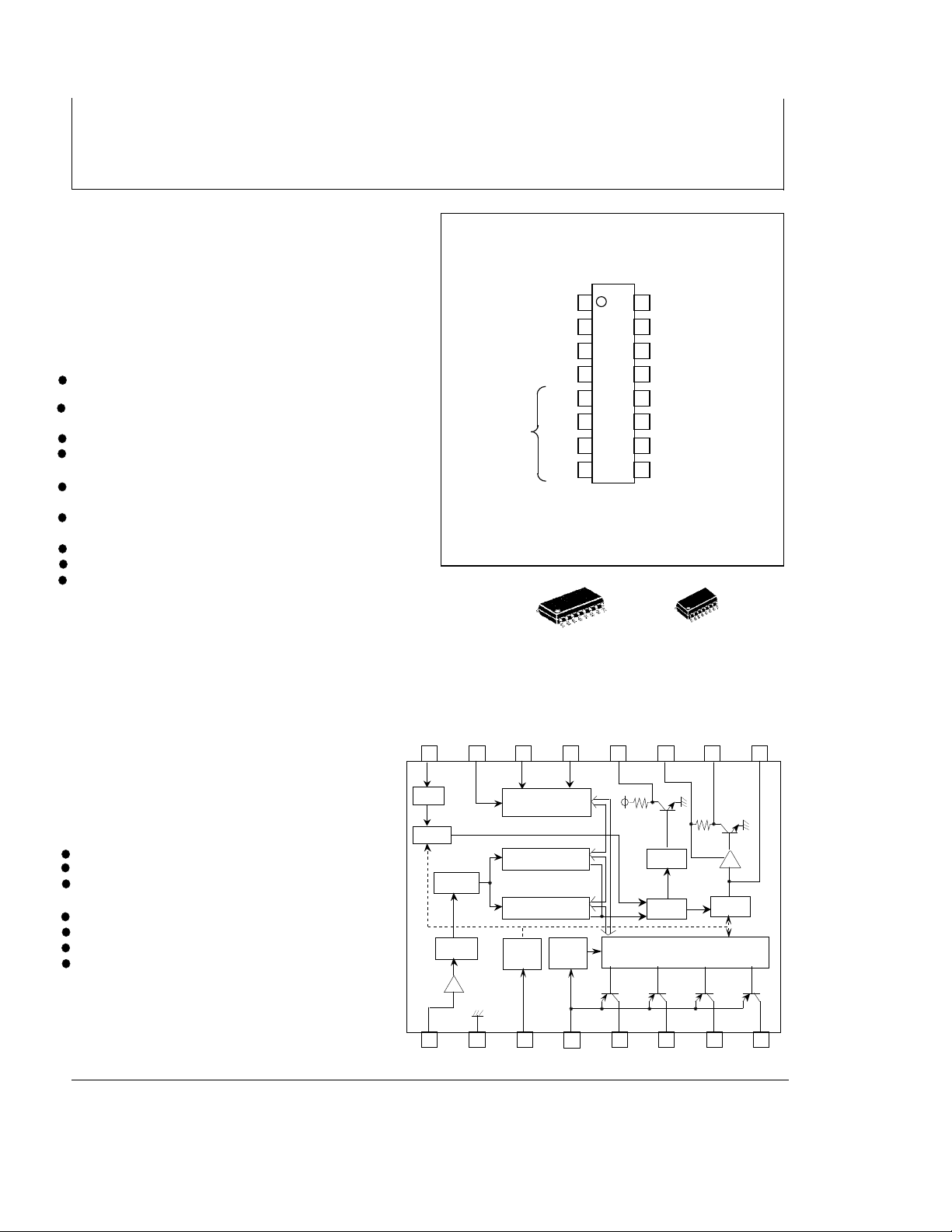
PIN CONFIGURATION (TOP VIEW)
PRESCALER INPUT fin
GND GND
SUPPLY VOLTAGE 1 Vcc1
SUPPLY VOLTAGE 2 Vcc2
BS4
BAND SWITCHING
OUTPUTS
BS3
BS2
BS1
OUTLINE 16P2S/16P2Z
1
2
3
4
5
6
7
8
16
15
14
13
12
11
10
9
CRYSTAL
Xin
OSCILLATOR
ENA ENABLE INPUT
DATA DATA INPUT
CLK CLOCK INPUT
LD/ f test LD/ f test OUTPUT
Vcc3 SUPPLY VOLTAGE 3
Vtu TUNING OUTPUT
Vin FILTER INPUT
Application
TV,VCR tuners
Recommended operating condition
Supply voltage range • • Vcc1=4.5 to 5.5V
Vcc2=Vcc1 to 13.2V
Vcc3=28 to 35V
Rated supply voltage • • Vcc1=5.0V
Vcc2=12V
Vcc3=33V
Function
1/32,1/33 dual-modulus prescaler
4MHz crystal oscillator,reference divider
Programmable divider
(10-bit M counter,5-bit S counter)
Tri-state phase comparator
Lock detector
Band switch driver
Op. Amp for direct tuning
16P2S
16P2Z
Block diagram
Bias
10
5
LD/
f test
Vcc1
4
Vcc3 Vtu Vin
10111213141516
LOCK
DETECTOR
PHASE
DETECTOR
BAND DRIVER
CHARGE
PUMP
XIN ENA DATA CLK
OSC
DIVIDER
1/32,1/33
1/8
1 2 3 4 5 6 7 8
19-BIT SHIFT
RESISTER LATCH
10-BIT M COUNTER
5-BIT S COUNTER
P.O.
reset
fIN GND Vcc1 Vcc2 BS4 BS3 BS2 BS1
9
MITSUBISHI
1
-12

Pin description
MITSUBISHI BIPOLAR DIGITAL ICs
M64893AFP/AGP
SERIAL INPUT PLL FREQUENCY SYNTHESIZER FOR TV/VCR
Symbol
f in
GND
Vcc1
Vcc2
BS4
BS3
BS2
BS1
Vin
Vtu
Vcc3
LD/ f test
CLOCK
DATA
ENABLE
X in
Pin No.
1
2
3
4
5
6
7
8
9
10
11
12
13
14
15
16
Pin name
Prescaler input
GND
Power supply voltage 1
Power supply voltage 2
Band switching
outputs
Filter input
(Charge pump output)
Tuning output
Power supply voltage 3
Lock detect/ Test port
Clock input
Data input
Enable input
This is connected to the
crystal oscillator.
Function
Input for the VCO frequency.
Ground to 0V.
Power supply voltage terminal. 5.0 ±0.5V
Power supply for band switching,Vcc1 to 13.2V
PNP open collector method is used.
When the band switching data is "H",the output is ON.
When it is "L",the output is OFF.
This is the output terminal for the LPF input and charge
pump output. When the phase of the programmable divider
output ( f 1/N) is ahead compared to the reference
frequency (fref), the "source" current state becomes active.
If it is behind, the "sink" current becomes active.
If the phases are the same, the high impedance state
becomes active.
This supplies the tuning voltage.
Power supply voltage for tuning voltage 28 to 35V
When 19 bit data is input,lock detector is output.
When 27 bit data is input, lock detector is output,
the programmable freq. Divider output and reference freq.
Output is selected by the test mode.
Data is read into the shift register when the clock signal falls.
Input for band SW and programmable freq. divider set up.
This is normally at a "L". When this is at "H", data and clock
signals are received. Data is read into the latch when the 19th
pulse of the clock signal falls.
4.0MHz crystal oscillator is connected.
MITSUBISHI
-12
2

MITSUBISHI BIPOLAR DIGITAL ICs
M64893AFP/AGP
SERIAL INPUT PLL FREQUENCY SYNTHESIZER FOR TV/VCR
Method of setting data
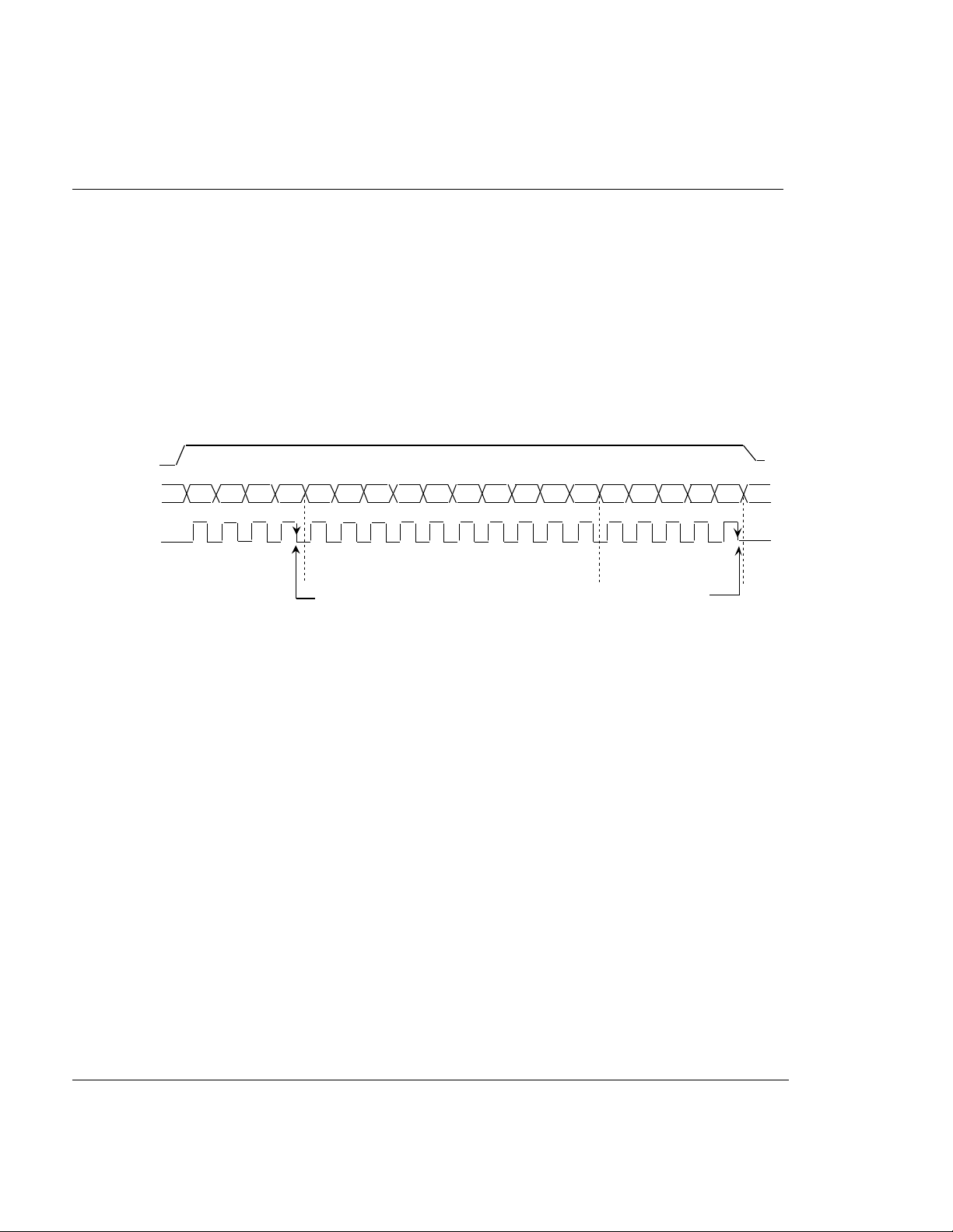
The frequency demultiplying ratio uses 15bits. Setting up the band switching output uses 4bits.
The test mode data uses 8bits. The total bits used is 27bits.Data is read in when the enable signal is "H" and
the clock signal falls.
The band switching data is read in at the 4th pulse of the clock signal.The program counter data is read into
the latch by the fall of the 19th pulse of the clock signal. When the enable signal goes to "L" before the 19th
pulse of the enable signal, only the band SW data is updated and other data is ignored.
The data is latched at the 19th pulse of the clock signal. At this time, 1/640 frequency division ratio is
used. Clock signals after the above are invalid.
E N A
27BS4 BS3 BS2 BS1
D A T A
28
M8 M7 M6 M5 M4 M3 M2 M1 M0 S4 S3 S2 S1 S0M9
26
25
24 23 22 21 20 24 23 22 21 2029
C L K
BAND SW
DATA
M COUNTER DIVISION
RATIO SETTING
READ INTO LATCH
S COUNTER DIVISION
RATIO SETTING
READ INTO LATCH
How to set the dividing ratio of the programmable divider
Total division N is given by the following formulas in addition to the prescaler used in the previous stage.
N=8 • (32M + S) M : 10 bit main counter division
S : 5 bit swallow counter division
The M and S counters are binary the possible ranges of division are as follows.
32 ≤ M ≤ 1023
O ≤ S ≤ 31
Therefore,the range of division N is 8,192 to 262,136.
The tuning frequency f VCO is given in the following equations.
f VCO= f REF x N
=6.25 x 8 x (32M + S)
=50.0 x (32M + S) [ kHz ]
But,the tuning frequency range is 51.2MHz to 1300Mz from the maximum prescaler operating
frequency.
MITSUBISHI
-12
3

MITSUBISHI BIPOLAR DIGITAL ICs
M64893AFP/AGP
SERIAL INPUT PLL FREQUENCY SYNTHESIZER FOR TV/VCR
Test mode data set up method
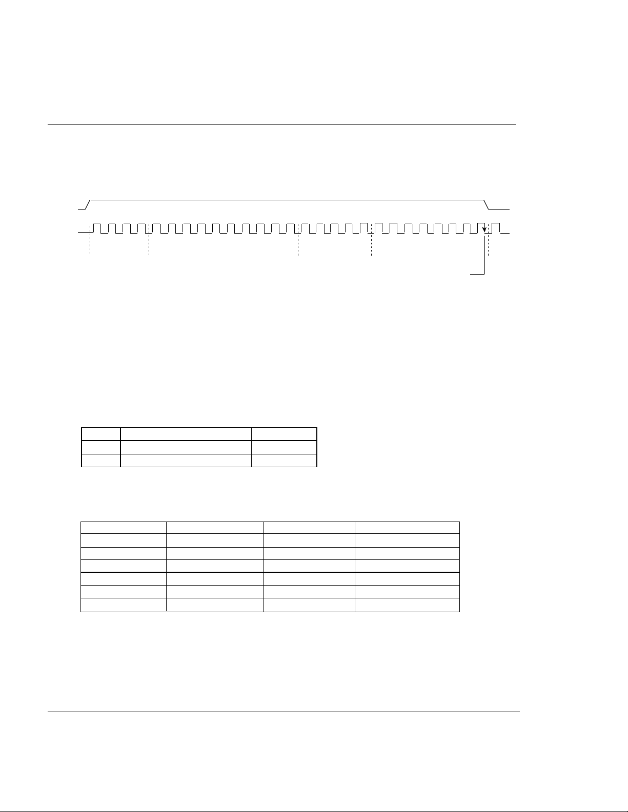
The data for the test mode uses 20 to 27bits. Data is latched when the 27th clock signal falls.
(1) When transferring 3-wire 27 bit data
ENA
1
CLK
BAND SW
DATA
(2) Test Mode Bit Set Up
X :Random, 0 or 1.normal "0"
CP :Set up the charge pump current value
T0, T1,&T2 :Set up test modes
RSa, Rsa :Set up for the reference Frequency division ratio
OS :Set up the tuning amplifier
S I :1 Only (It is prohibit to "0 ")
M COUNTER DIVISION
RATIO SETTING
S COUNTER
DIVISION RATIO
SETTING
19 20 27
SI
CP T2 T1 TO
TEST DATA SETTING
READ INTO LATCH
RSa RSbOS
Setting up the charge pump current of the phase comparator
CP
0
1
Charge pump current
70 uA
270 uA
Mode
Test
Normal
Setting up for the test mode
T2 T1 T0
0 0 X
0 1 X
1 1 0
1 1 1
1 0 0
1 0 1
Charge pump
Normal operation
High impedance
Sink
Source
High impedance
High impedance
12 pin output
LD
LD
LD
LD
fREF
f1/N
Mode
Normal operation
Test mode
Test mode
Test mode
Test mode
Test mode
MITSUBISHI
4
-12
 Loading...