

MITSUBISHI BIPOLAR DIGITAL ICs
New Product
SERIAL INPUT PLL FREQUENCY SYNTHESIZER FOR TV/VCR
Description
The M64893AFP/AGP is a semiconductor integrated
circuit consisting of PLL frequency synthesizer for
TV/VCR using Bip process. It contains the prescaler with
operating up to1.3GHz,4 band drivers and Op.Amp for
direct tuning.
Features
4 integrated PNP band drivers
(Io=40mA,Vsat=0.2V typ@Vcc1 to 13.2V )
Built-in Op.Amp for direct tuning voltage
output (33V)
Low power dissipation (Icc=20mA,Vcc1=5V)
Built-in prescaler with input amplifier
(Fmax=1.3GHz)
PLL lock/unlock status display out put
(Built-in pull up resistor )
X`tal 4MHz is used to realize 1 type of tuning
steps (Division ratio 1/640)
Serial data input (3 wire bus )
Built-in Power on reset system
Small Package(16SOP/16SSOP)
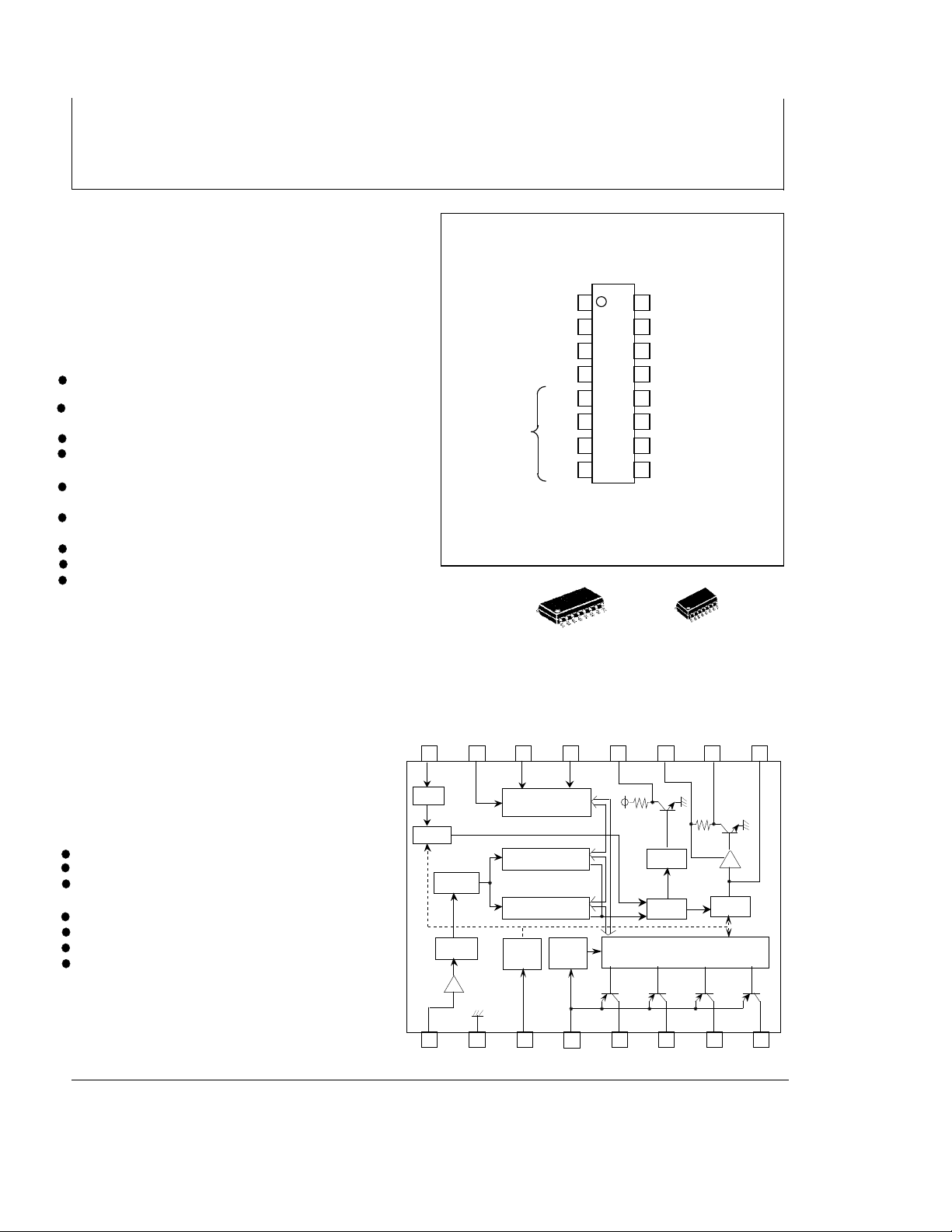
M64893AFP/AGP
PIN CONFIGURATION (TOP VIEW)
PRESCALER INPUT fin
GND GND
SUPPLY VOLTAGE 1 Vcc1
SUPPLY VOLTAGE 2 Vcc2
BS4
BAND SWITCHING
OUTPUTS
BS3
BS2
BS1
OUTLINE 16P2S/16P2Z
1
2
3
4
5
6
7
8
16
15
14
13
12
11
10
9
CRYSTAL
Xin
OSCILLATOR
ENA ENABLE INPUT
DATA DATA INPUT
CLK CLOCK INPUT
LD/ f test LD/ f test OUTPUT
Vcc3 SUPPLY VOLTAGE 3
Vtu TUNING OUTPUT
Vin FILTER INPUT
Application
TV,VCR tuners
Recommended operating condition
Supply voltage range • • Vcc1=4.5 to 5.5V
Vcc2=Vcc1 to 13.2V
Vcc3=28 to 35V
Rated supply voltage • • Vcc1=5.0V
Vcc2=12V
Vcc3=33V
Function
1/32,1/33 dual-modulus prescaler
4MHz crystal oscillator,reference divider
Programmable divider
(10-bit M counter,5-bit S counter)
Tri-state phase comparator
Lock detector
Band switch driver
Op. Amp for direct tuning
16P2S
16P2Z
Block diagram
Bias
10
5
LD/
f test
Vcc1
4
Vcc3 Vtu Vin
10111213141516
LOCK
DETECTOR
PHASE
DETECTOR
BAND DRIVER
CHARGE
PUMP
XIN ENA DATA CLK
OSC
DIVIDER
1/32,1/33
1/8
1 2 3 4 5 6 7 8
19-BIT SHIFT
RESISTER LATCH
10-BIT M COUNTER
5-BIT S COUNTER
P.O.
reset
fIN GND Vcc1 Vcc2 BS4 BS3 BS2 BS1
9
MITSUBISHI
1
-12
Pin description
MITSUBISHI BIPOLAR DIGITAL ICs
M64893AFP/AGP
SERIAL INPUT PLL FREQUENCY SYNTHESIZER FOR TV/VCR
Symbol
f in
GND
Vcc1
Vcc2
BS4
BS3
BS2
BS1
Vin
Vtu
Vcc3
LD/ f test
CLOCK
DATA
ENABLE
X in
Pin No.
1
2
3
4
5
6
7
8
9
10
11
12
13
14
15
16
Pin name
Prescaler input
GND
Power supply voltage 1
Power supply voltage 2
Band switching
outputs
Filter input
(Charge pump output)
Tuning output
Power supply voltage 3
Lock detect/ Test port
Clock input
Data input
Enable input
This is connected to the
crystal oscillator.
Function
Input for the VCO frequency.
Ground to 0V.
Power supply voltage terminal. 5.0 ±0.5V
Power supply for band switching,Vcc1 to 13.2V
PNP open collector method is used.
When the band switching data is "H",the output is ON.
When it is "L",the output is OFF.
This is the output terminal for the LPF input and charge
pump output. When the phase of the programmable divider
output ( f 1/N) is ahead compared to the reference
frequency (fref), the "source" current state becomes active.
If it is behind, the "sink" current becomes active.
If the phases are the same, the high impedance state
becomes active.
This supplies the tuning voltage.
Power supply voltage for tuning voltage 28 to 35V
When 19 bit data is input,lock detector is output.
When 27 bit data is input, lock detector is output,
the programmable freq. Divider output and reference freq.
Output is selected by the test mode.
Data is read into the shift register when the clock signal falls.
Input for band SW and programmable freq. divider set up.
This is normally at a "L". When this is at "H", data and clock
signals are received. Data is read into the latch when the 19th
pulse of the clock signal falls.
4.0MHz crystal oscillator is connected.
MITSUBISHI
-12
2
MITSUBISHI BIPOLAR DIGITAL ICs
M64893AFP/AGP
SERIAL INPUT PLL FREQUENCY SYNTHESIZER FOR TV/VCR
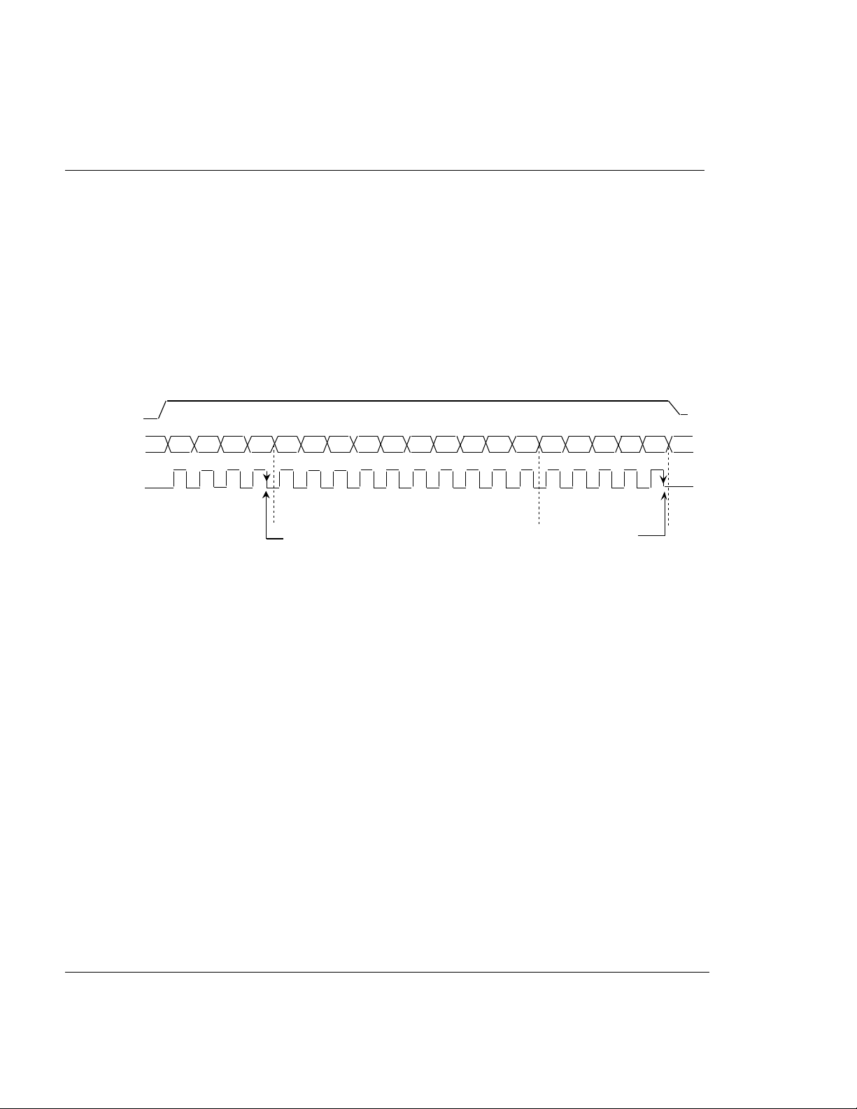
Method of setting data
The frequency demultiplying ratio uses 15bits. Setting up the band switching output uses 4bits.
The test mode data uses 8bits. The total bits used is 27bits.Data is read in when the enable signal is "H" and
the clock signal falls.
The band switching data is read in at the 4th pulse of the clock signal.The program counter data is read into
the latch by the fall of the 19th pulse of the clock signal. When the enable signal goes to "L" before the 19th
pulse of the enable signal, only the band SW data is updated and other data is ignored.
The data is latched at the 19th pulse of the clock signal. At this time, 1/640 frequency division ratio is
used. Clock signals after the above are invalid.
E N A
27BS4 BS3 BS2 BS1
D A T A
28
M8 M7 M6 M5 M4 M3 M2 M1 M0 S4 S3 S2 S1 S0M9
26
25
24 23 22 21 20 24 23 22 21 2029
C L K
BAND SW
DATA
M COUNTER DIVISION
RATIO SETTING
READ INTO LATCH
S COUNTER DIVISION
RATIO SETTING
READ INTO LATCH
How to set the dividing ratio of the programmable divider
Total division N is given by the following formulas in addition to the prescaler used in the previous stage.
N=8 • (32M + S) M : 10 bit main counter division
S : 5 bit swallow counter division
The M and S counters are binary the possible ranges of division are as follows.
32 ≤ M ≤ 1023
O ≤ S ≤ 31
Therefore,the range of division N is 8,192 to 262,136.
The tuning frequency f VCO is given in the following equations.
f VCO= f REF x N
=6.25 x 8 x (32M + S)
=50.0 x (32M + S) [ kHz ]
But,the tuning frequency range is 51.2MHz to 1300Mz from the maximum prescaler operating
frequency.
MITSUBISHI
-12
3
MITSUBISHI BIPOLAR DIGITAL ICs
M64893AFP/AGP
SERIAL INPUT PLL FREQUENCY SYNTHESIZER FOR TV/VCR
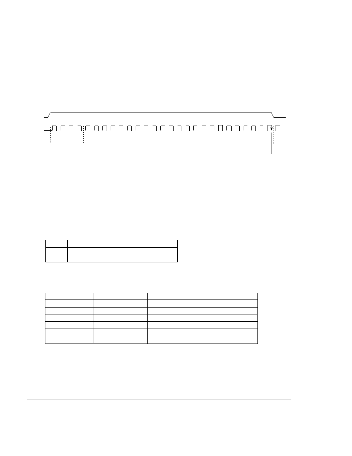
Test mode data set up method
The data for the test mode uses 20 to 27bits. Data is latched when the 27th clock signal falls.
(1) When transferring 3-wire 27 bit data
ENA
1
CLK
BAND SW
DATA
(2) Test Mode Bit Set Up
X :Random, 0 or 1.normal "0"
CP :Set up the charge pump current value
T0, T1,&T2 :Set up test modes
RSa, Rsa :Set up for the reference Frequency division ratio
OS :Set up the tuning amplifier
S I :1 Only (It is prohibit to "0 ")
M COUNTER DIVISION
RATIO SETTING
S COUNTER
DIVISION RATIO
SETTING
19 20 27
SI
CP T2 T1 TO
TEST DATA SETTING
READ INTO LATCH
RSa RSbOS
Setting up the charge pump current of the phase comparator
CP
0
1
Charge pump current
70 uA
270 uA
Mode
Test
Normal
Setting up for the test mode
T2 T1 T0
0 0 X
0 1 X
1 1 0
1 1 1
1 0 0
1 0 1
Charge pump
Normal operation
High impedance
Sink
Source
High impedance
High impedance
12 pin output
LD
LD
LD
LD
fREF
f1/N
Mode
Normal operation
Test mode
Test mode
Test mode
Test mode
Test mode
MITSUBISHI
4
-12

SERIAL INPUT PLL FREQUENCY SYNTHESIZER FOR TV/VCR
Set up for the reference Frequency division ratio
MITSUBISHI BIPOLAR DIGITAL ICs
M64893AFP/AGP
RSa RSb
1 1
0 1
X 0
Division ratio
1/ 512
1/ 1024
1/ 640
Set up the tuning amplifier
OS
0
1
Tuning voltage out put
ON
OFF
Mode
Normal
Test
Power on reset operation (Initial state the power is turned ON)
BS4 to BS1 : OFF
Charge pump : High impedance
Tuning amplifier : OFF
Charge pump current : 270uA
Frequency division ratio : 1/640
Lock detect : H
MITSUBISHI
-12
5

Timing diagram
MITSUBISHI BIPOLAR DIGITAL ICs
M64893AFP/AGP
SERIAL INPUT PLL FREQUENCY SYNTHESIZER FOR TV/VCR
tr
ENABLE
10%
90%
1.5V
tINT
DATA
CLOCK
1.5V
tSU(E)
tPWC
tSU(D)
90%
1.5V
10%
tH(D)
Crystal oscillator connection diagram
90%
10%
tr tf
90%
10%
tftr
90%
tH(E)
90%
tINT
10%
tf
10%
tBCL
VIH
VIL
tBT
VIH
VIL
VIH
VIL
16
18pF
4MHz
Crystal oscillator characteristics
Actual resistance : less than 3 0 0 Ω
Load capacitance : 2 0 p F
MITSUBISHI
-12
6

MITSUBISHI BIPOLAR DIGITAL ICs
M64893AFP/AGP
SERIAL INPUT PLL FREQUENCY SYNTHESIZER FOR TV/VCR
Absolute maximum ratings (Ta=-20°C to +75°C unless otherwise noted)
Parameter
Supply voltage 1
Supply voltage 2
Supply voltage 3
Input voltage
Output voltage
Voltage applied when
the band output is OFF
Band output current
ON the time when the
band output is ON
Power dissipation
Operating temperature
Storage temperature
Symbols
Vcc1
Vcc2
Vcc3
VI
Vo
VBSOFF
IBSON
tBSON
Pd
Topr
Tstg
Max.ratings
6.0
14.4
36.0
6.0
6.0
14.4
50.0
10
470
-20 to +75
-40 to +125
Units
V
V
V
V
V
V
mA
sec
mW
°C
°C
Conditions
Pin3
Pin4
Pin11
Not to exceed Vcc1
LD output
per 1 band output circuit
50mA per 1 band output circuit
3circuits are pn at same time,
Ta= +75°C
Recommended operating conditions (Ta=-20°C to +75°Cunless otherwise noted)
Parameter
Supply voltage 1
Supply voltage 2
Supply voltage 3
Operating frequency (1)
Operating frequency (2)
Band output current 5 to 8
Symbol
Vcc1
Vcc2
Vcc3
fopr1
fopr2
IBDL
Ratings
4.5 to 5.5
Vcc1 to 13.2
28 to 35
4.0
80 to 1,300
0 to 40
Conditions
Units
V
Pin3
V
Pin4
V
Pin11
MHz
Crystal oscillation circuit
MHz
mA
Normally 1 circuit is on. 2 circuits on at the
same time is max. It is prohibited to have
3 or more circuits turned on at the same
time.
MITSUBISHI
-12
7

MITSUBISHI BIPOLAR DIGITAL ICs
M64893AFP/AGP
SERIAL INPUT PLL FREQUENCY SYNTHESIZER FOR TV/VCR
Electrical characteristics (Ta=-20°C to +75°C unless otherwise noted)
Vcc1=5.0V, Vcc=12V, Vcc3=33V
Parameters
Input terminals
"H"input voltage
"L"input voltage
"H"input current
"L"input current
"L"input current
Lock output
"H"output voltage
"L"output voltage
Band SW
output voltage
Leak current
Tuning output
output voltage "H"
output voltage "L"
Charge pump
"H" output current
"L" output current
Leak current
Supply current 1
Supply current 2
4 circuits OFF
1 circuits ON,
Output open
Output current 40mA
Supply current 3
Symbol
VIH
VIL
IIH
IIL
IIL
VOH
VOL
VBS
IOlk2
VtoH
VtoL
ICPH
ICPL
IcpLK
Icc1
Icc2A
Icc2B
Icc2C
Icc3
Test pin
13 to 15
13 to 15
13 to 15
13,15
14
12
12
5 to 8
5 to 8
10
10
9
9
9
3
4
4
4
11
Test conditions
Vcc1=5.5V ,Vi=4.0V
Vcc1=5.5V,Vi=0.4V
Vcc1=5.5V ,Vi=0.4V
Vcc1=5.5V
Vcc1=5.5V
Vcc2=12V Io=-40mA
Vcc2=12V Band SW is OFF
Vcc3=33V
Vcc3=33V
Vcc1=5.0V Vo=1V
Vcc1=5.0V Vo=1V
Vcc1=5.0V Vo=2.5V
Vcc1=5.5V
Vcc2=12V
Vcc2=12V
Vcc2=12V Io=-40mA
Vcc3=33V Output ON
Limits
Min Typ Max
3.0 - Vcc1+0.3
- - 1.5
- - 10
- -6 -10
- -18 -30
5.0 - -
- 0.3 0.5
11.6 11.8 -
- - -10
32.5 - -
- 0.2 0.4
- ±270 ±370
- ±70 ±110
- - ±50
- 20 30
- - 0.3
- 6.0 8.0
- 46.0 48.0
- 3.0 4.0
Unit
V
V
uA
uA
uA
V
V
V
uA
V
V
uA
uA
nA
mA
mA
mA
mA
mA
The typical values are at Vcc1=5V,Vcc2=12V,Vcc3=33V,Ta=+25°C
MITSUBISHI
-12
8

MITSUBISHI BIPOLAR DIGITAL ICs
M64893AFP/AGP
SERIAL INPUT PLL FREQUENCY SYNTHESIZER FOR TV/VCR
Switching characteristics (Ta=-20°C to +75°C unless otherwise noted)
Vcc1=5.0V, Vcc2=12V, Vcc3=33V
Parameter
Prescaler operating
frequency
Operating input
voltage
Clock pulse width
Data setup time
Data hold time
Enable setup time
Enable hold time
Enable data interval
time
Rise time
Fall time
Next enable prohibit
time
Next clock prohibit
time
Symbol
f opr2
V in
t PWC
t SU(D)
t H(D)
t SU(E)
t H(E)
t INT
t r
t f
t BT
t BCL
Test pin
1
1
13
14
14
15
15
15,14
13,14,15
13,14,15
15
13,15
Test conditions
Vcc1=4.5 to 5.5V
Vin=Vinmin to Vinmax
Vcc1=4.5 80 to 100MHz
to 5.5V 100 to 200MHz
200 to 800MHz
800 to 1000MHz
1000 to 1300MHz
Vcc1=4.5 to 5.5V
Vcc1=4.5 to 5.5V
Vcc1=4.5 to 5.5V
Vcc1=4.5 to 5.5V
Vcc1=4.5 to 5.5V
Vcc1=4.5 to 5.5V
Vcc1=4.5 to 5.5V
Vcc1=4.5 to 5.5V
Vcc1=4.5 to 5.5V
Vcc1=4.5 to 5.5V
Limits
Min. Typ Max
80 - 1300
- 24 - 4
- 27 - 4
- 30 - 4
- 27 - 4
- 18 - 4
1 - -
2 - -
1 - -
3 - -
3 - -
1 - -
- - 1
- - 1
5 - -
5 - -
Unit
used
MHz
dBm
us
us
us
us
us
us
us
us
us
us
MITSUBISHI
-12
9

Application example
+
1000pF
MCU
10µ
-
14
13
15
12
+5V
1
3
4
2
20
16
5
T E S T
M5493X
series
DATA
CLK
EN
LD
/ f1/N
X
IN XOUT
6
18p
4MHz
MITSUBISHI BIPOLAR DIGITAL ICs
M64893AFP/AGP
SERIAL INPUT PLL FREQUENCY SYNTHESIZER FOR TV/VCR
BUILT-IN PLL TUNER
+5V
3
18
Vcc2SW
B S 4
B S 3
B S 2
B S 1
G N D
PD
G N D
7 8
M64893AFP / AGP
47k
11
47k
12
47k
13
47k
14
fIN
17
16
15
10
9
1000
ÇêÇe
11
+
-
4
5
6
7
8
0.1u
9
10
+ 3 3 V
Vcc1 to 12V
+
-
+B
BS4
BS3
BS2
BS1
1000pF
1.5n
56K
56K
100P
Note)Filter constant is for reference.
Add a capacitor to stabilize the circuit.
*
Lo
VT
2.2n
*
UHF
4-BAND
TUNER
AFT
VHF
AGC
IF
IF
AGC
B T
MITSUBISHI
10
-12

SERIAL INPUT PLL FREQUENCY SYNTHESIZER FOR TV/VCR
Marking DWG ( M 6 4 8 9 3 A F P )
8 9 3 A F P
MITSUBISHI BIPOLAR DIGITAL ICs
M64893AFP/AGP
X X X X
L o t No,
External appearance
16P2S type <16pin plastic mold SOP> Unit:mm
16
1
1.27±0.15
9
8
0.4
+0.1
-0.05
10.0±0.2
0.15
0.05
+0.05
-0.02
MITSUBISHI
11
-12

SERIAL INPUT PLL FREQUENCY SYNTHESIZER FOR TV/VCR
Marking DWG ( M 6 4 8 9 3 A G P )
8 9 3 A
X X X
MITSUBISHI BIPOLAR DIGITAL ICs
M64893AFP/AGP
Lot No,
External appearance
16P2Z type <16pin plastic mold SSOP> Unit:mm
16
1
1.9
0.65±0.12
5.0±0.2
9
8
0.22
+0.1
-0.05
4.4±0.1
1.5
0.15
+0.05
-0.02
0.05
6.2±0.2
0.5±0.2
0.1
MITSUBISHI
12
-12
 Loading...