

Transistor for VCO,1st IF MIX,2-multiple circuit built-in 500MHz/1GHz Dual PLL Synthesizer
Ver 1.0
Nov 25,1998
ELECTRIC
•
Software is compatible with
SWSWSW
SW
SW
SWSWSW
To TX.VCO
micro computer
LOCAL
DATA
Output
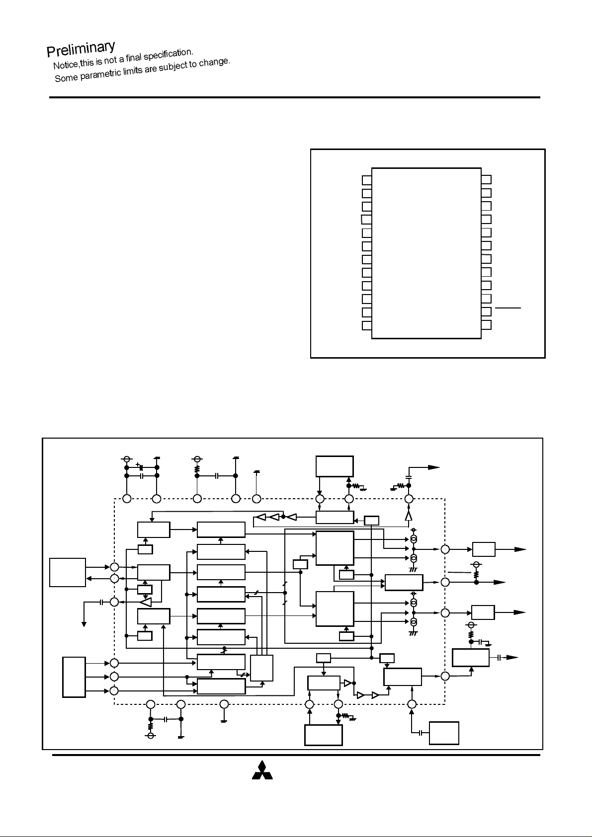
1.DESCRIPTION
The M64884FP is a 2-system 1-chip PLL frequency synthesizer IC designed of Analog cordless telephone for North
America (ISM band) that can directly enter signal up to 500MHz in the TX and up to 1GHz in the RX.
Adoption of high performance Bi-CMOS process enables low
power consumption type 2-modulus prescaler to be built in
TXGND1
the IC to directly signal enter up to 500MHz in the TX and up
to 1GHz in the RX.This IC also contains VCO oscillation-Tr in
the TX and RX,2-multiple circuit for transmission output and
double balance type mixer for the 1st intermediate frequency
(1st IF).
TXGND2
2.FEATURES
•
Low power current Icc=24mA. (@Vcc=3.0V,at TX/RX VCO
and 2-multiple circuit output current=2mA setting)
•
Built-in 2-modulus prescaler.
• input frequency --- TX:350~500MHz,RX:700~1000MHz.
• input sensitivity --- -15 ~ -5dBm.
•
Built-in buffer-Tr for oscillation circuit in the TX and RX.
•
Built-in 2-multiple circuit for transmission output.
•
Built-in double balance type mixer for the 1st IF.
•
Rated current output type charge pump. Output current can
be set with serial data. (100,300,500,700µA)
•
Built-in B-E Colpitts type oscillation circuit for standard oscillation.
M64084AGP.
MITSUBISHI ICs (Cordless Telephone)
M64884FP
1
TXOUT
TXVCC
TXB
TXE
PD1
VCC
XIN
XOUT
XBO
GND
Outline 24SSOP (0.65 milli-pitch)
2
3
4
5
6
7
8
9
10
11
12
APPLICATION
900MHz analog cordless telephone
(ISM band)
24
23
22
21
20
19
18
17
16
15
14
MIXIN
MIXGND
RXVCC
RXB
RXE
RXGND
PD2
RST
SI
CPS
LOCK
MIXOUT13
3.BLOCK DIAGRAM
VCC
8 3
To
2nd.MIX
Input
XIN
XOUT
XBO
SI
CPS
RST
9
10
11
16
15
17
RXVCC
standard
oscillation
circuit
GND
1/16,17
Prescaler
OSC+1/2
Divider
1/32,33
Prescaler
12
TXVCC
1922
RXGND
TXGND2
Programmable
Divider
17
L a t c h
Programmable
Divider
13
L a t c h
Programmable
Divider
17
L a t c h
Shift Resister
Pulse Counter
23
TX.VCO
Circuit
TXGND1 TXB
6
1 4 5 2
1/2
2
4
2
2
Latch
2
Select
MIXGND
RXB RXE
TXE
VCO(TX)
P h a s e
Detector
P h a s e
Detector
VCO(RX)
21
RX.VCO
Circuit
detector
MIXIN
Lock
MIX
TXOUT
x2
2420
TX 2-multiple output
(To TXAMP)
PD1
7
14
18
13
LNA
Circuit
LOCK
PD2
Tank
Load
MIXOUT
LPF
To
LPF
To RX.VCO
1st.IF
MITSUBISHI
1
Transistor for VCO,1st IF MIX,2-multiple circuit built-in 500MHz/1GHz Dual PLL Synthesizer
Ver 1.0
Nov 25,1998
ELECTRIC
2
4. PIN Description
MITSUBISHI ICs (Cordless Telephone)
M64884FP
1 TXGND1
TXVCC3
4 TXB
5
TXE
6
7
8
9
PD1
VCC
XIN
XOUT10
11
XBO
12 GND
14
15
LOCK
CPS
16
17
18
19
20
21
RST
PD2
RXGND
RXE
RXB
RXVCC22
23
MIXGND
24 MIXIN
Pin NameSymbolPin No.
1st ground for transmission system. 0V.Transmission system ground 1
Transmission outputTXOUT2
Transmission circuit base Base pin of the transmission VCO transistor.
Transmission circuit emitter
Transmission system
Charge Pump output
Crystal oscillator input
Ground Ground pin for the PLL system. 0V.
Reception system
Charge Pump Output
Reception circuit emitter
Mixer input Mixer signal input pin.
Output frequency that multiples the oscillation frequency of the transmission
system by 2, and outputs an open emitter.
Power supply pin for transmission VCO circuit. TXVCC = 2.7~3.6V.Transmission system power supply
Emitter pin of the transmission VCO transistor. Set the current of the transmission oscillation circuit by pull-down resistance.
2nd ground for transmission system. 0V.Transmission system ground 2TXGND2
Output the set current according to the difference in phase between Charge
Pump output pins in the PLL1(TX) system.
HiZ with the power supply turned off.
Power supply pin for the PLL system. VCC = 2.7~3.6V. Power supply
Inputs 4 to 25MHz output from the base oscillator to the XIN .
External crystal oscillator is available for oscillation.
Buffer output pin of base oscillation.Buffer output
Extracts IF frequencies.Mixer OutputMIXOUT13
Judgment is made in a system turned on when the other system is turned off.Lock detection output
Operates at the rising edge of the clock pulse of the shift resistor.Clock pulse input
Inputs serial data.Data inputSI
Inputs the reset pulse of 21 pulse counters.Reset pulse input
Output the set current according to the difference in phase between Charge
Pump output pins in the PLL2(RX) system.
HiZ with the power supply turned off.
Ground for reception system. 0V.Reception system ground
Emitter pin of the reception VCO transistor. Set the current of the reception
oscillation circuit by pull-down resistance.
Base pin of the reception VCO transistor.Reception circuit base
Power supply pin for reception VCO circuit. TXVCC = 2.7~3.6V. Reception system power supply
Ground for mixer system. 0V.Mixer system ground
Functions
MITSUBISHI

Transistor for VCO,1st IF MIX,2-multiple circuit built-in 500MHz/1GHz Dual PLL Synthesizer
Ver 1.0
Nov 25,1998
ELECTRIC
MSB
Shift register
Power ON/OFF
Latch selection
Charge
Set
Division ratio for reference (13 bits)
LSB
Charge
Set
Division ratio for local oscillator 1(17 bits)
Division ratio for local oscillator 2(17 bits)
Note 1) At the positive edge of CPS input, SI input status is read into the shift resistor in sequence.
CPS
ALID
ALID
D19
D18
D1
D2
SI
D21
D20
RST
MSB
LSB
VIH = 0.7*VCC ~ 3.6 (V)
Effective data
tSUthtWH
tWL
tSU = th = tWH = tWL > 0.5 µs
tCR = tRH = tRC > 1 µs
SI
CPS
tCR
tRH
tRC
RST
12202162021620
5. Functional Description
(1) Data Entry
Note 2) All data is set at the positive edge of the 21st pulse. After that, CPS is invalid.
Note 3) While RST is set to "H", neither CPS nor SI is received.
(2) Input Signal Timing
MITSUBISHI ICs (Cordless Telephone)
M64884FP
INV-
INV-
(3) Input Voltage
VIL = -0.2 ~ 0.3*VCC (V)
(4) Shift Resister Bit Configuration
DCDD
DADB
Pump 2
Current
DHDGDFDE
Pump 1
Current
123456789101112131415161718192021
2
MITSUBISHI
3

MITSUBISHI ICs (Cordless Telephone)
Ver 1.0
Nov 25,1998
ELECTRIC
M64884FP
Transistor for VCO,1st IF MIX,2-multiple circuit built-in 500MHz/1GHz Dual PLL Synthesizer
Note 4) DD and DC are used to turn on/off the power supply to the PLL system.
Data
DCDD
LL
HL
LH
HH
Note 5) DB and DA are used to select data latch to be updated.
Data
DADB
LL
HL
LH
HH
Note 6) DE/DF and DG/DH are used to set the current of charge pump.
Both two PLLs are on.
Only PLL of local oscillator 1 is on.
Only PLL of local oscillator 2 is on.
Both two PLLs are off.
Testing mode only. Inhibited from use.
Updates data of local oscillator 1.
Updates data of local oscillator 2.
Updates data for comparison frequency.
Description
Description
DE
DG
L
L
H
H
Note 7) Current supplied to the charge pump for local oscillators 1 and 2 can be set independently in systems.
However,when power supply is turned off, the charge pump output is placed in "HiZ" status regardless
of set value.
Note 8) The division ratio of the programmable divider for comparison frequency is given in 13-bit binary code.
For transmission local oscillator N(Fref) = 4 * P However, P = 20 to 8191
For reception local oscillator N(Fref) = 2 * P However, P = 20 to 8191
Note 9) The division ratio of programmable divider for local oscillators 1 and 2 are given in 17-bit binary code.
For transmission local oscillator N(FvcoTX) = 256 to 131071
For reception local oscillator N(FvcoRX) = 1024 to 131071
DF
DH
L
H
L
H
Output current value of charge pump
100µA
300µA
500µA
700µA
MITSUBISHI
4

Transistor for VCO,1st IF MIX,2-multiple circuit built-in 500MHz/1GHz Dual PLL Synthesizer
Ver 1.0
Nov 25,1998
ELECTRIC
6. X'tal OSCILLATION CIRCUIT
Connection of oscillation block.
Built-in buffer transistor for oscillation enables direct oscillation at X'tal.
Connections of X'tal and TCXO are shown below.(recommended circuit)
MITSUBISHI ICs (Cordless Telephone)
M64884FP
When X'tal is in use
X'tal
XIN
XOUT
C : CH type
When TCXO is in use
XIN
1000p
XOUT
7. Connection of Buffer Block
As the 2nd mixer local oscillator, the buffer output pin(XBO) is set to share X'tal. The pin is available as
follows.
When the pin is not shared
1000p
XBO
2nd MIX
When the pin is shared
XBO
1000p
TCXO
OPEN
8. Negative Resister Evaluation Circuit
Negative resistor in the oscillation circuit are measured with the conditions and coefficients shown in drawing
below.
X'tal
: 21.25MHz(TEW CORP CI = 20ohm)
C1
: 18 pF
C2
: 36 pF
C3
: 100 pF
C4
: 36 pF
Cv
: ~30 pF
VCC
: 3V
Ta
: 25oC
XIN
XOUT
R
C1
C2
C : CH type
X'tal
C4
MITSUBISHI
C3
Cv
5

Transistor for VCO,1st IF MIX,2-multiple circuit built-in 500MHz/1GHz Dual PLL Synthesizer
Ver 1.0
Nov 25,1998
ELECTRIC
9. Lock Detection, PD Output
Comparison
Frequency
Local Oscillator
division output
Source
PD output
MITSUBISHI ICs (Cordless Telephone)
M64884FP
Sink
1
LOCK output
Note 10) The PD output is placed in the "Source" status when the phase of local oscillator division output
is behind the phase comparison frequency. It is placed in the "Sink" status when the phase of
local oscillator division output advances.
11) " " means high impedance status.
12) When the phase difference that is 8 times or less* of the OSC frequency continues 15 or more
cycles of comparison frequency (Fref), LOCK output is placed in the "L" status.
(*625ns when a 12.8MHz oscillator is used)
13) When the power supply of each system is turned off, the LOCK output status goes to "H".
14) The LOCK output circuit is an open drain output of the N channel MOS transistor. Use this circuit
with pull-up.
2
3
14
15
MITSUBISHI
6

MITSUBISHI ICs (Cordless Telephone)
Ver 1.0
Nov 25,1998
ELECTRIC
M64884FP
Transistor for VCO,1st IF MIX,2-multiple circuit built-in 500MHz/1GHz Dual PLL Synthesizer
10. INPUT OUTPUT EQUIVALENT CIRCUIT
TXVCO(TXB, TXE, TXOUT)
TXB
TXE
OSC(XIN, XOUT, XBO) MIX(MIXIN, MIXOUT)
2K
TXOUT
4K
RXVCO(RXB, RXE)
RXB
RXE
Lo Lo
2K
MIXOUT
XIN
XOUT
6K
Charge Pump output(PD1, PD2)
1K
1K
PD1
PD2
XBO
MIXIN
Data input(SI, CPS, RST)
LOCK Detection output (LOCK)
SI
CPS
RST
LOCK
MITSUBISHI
7

MITSUBISHI ICs (Cordless Telephone)
Ver 1.0
Nov 25,1998
ELECTRIC
M64884FP
Transistor for VCO,1st IF MIX,2-multiple circuit built-in 500MHz/1GHz Dual PLL Synthesizer
11. ABSOLUTE MAXIMUM RATINGS (Ta=-30oC to +85oC, unless otherwise noted)
Vcc
Topr
Tstg
1000
Vo
Io
Vi
Pd
Tj
Supply Voltage
Output Voltage
Output Current
Input Voltage
Input Current
Ii
Power Consumption
Junction Temperature
Operating Ambient Voltage
Storage Ambient Voltage
Ratings
Max.Min.
GND=0V
LOCK, MIXOUT
TXE, RXE, TXOUT
SI, CPS, RST
LOCK, GND=0V
Ta=85oC, Tj=125oC
-0.3 4.5
4.50
0 6.0
4.5-0.3
0 1.0
232
125
85-30
125-40
Total Power Dissipation Delating Curve
RemarksUnitTest ConditionParameterSymbol
V
V
mA
V
mA
Package Allowable Power
mW
o
C
o
C
o
C
581
500
232
0
0
25 50 75 85
100
125 150
Temperature Ta (oC)
MITSUBISHI
8

MITSUBISHI ICs (Cordless Telephone)
Ver 1.0
Nov 25,1998
ELECTRIC
Transistor for VCO,1st IF MIX,2-multiple circuit built-in 500MHz/1GHz Dual PLL Synthesizer
12. RECOMMENDED OPERATING CONDITIONS
(Vcc=2.7 to 3.6V, Ta=-30oC to +85oC, unless otherwise noted)
Recommended
Vcc
Supply Voltage
Test ConditionParameterSymbol
GND=0V
2.7
Values
Max.Typ.Min.
3.63.0
M64884FP
PinUnit
VCC
V
TXVCC
RXVCC
PLoTX
PLoRX
FLoTX
FLoRX
VXIN
VXOUT
Fosc
PRFin
IOL
Transmission Local
Oscillation Amplitude
Reception Local
Oscillation Amplitude
Transmission Local
Oscillation Frequency
Reception Local
Oscillation Frequency
XIN Input Amplitude
XOUT Input Amplitude
Reference
Oscillation Frequency
MIXIN Input Amplitude
"L" Output Current
Electric Potential
between VCC and TXVCC
Electric Potential
between VCC and RXVCC
FLoTX=
350~500MHz
FLoRX=
700~1000MHz
PLoTX=
-15 ~ -5dBm
PLoRX=
-15 ~ -5dBm
Fosc=4~25MHz
Fosc=4~25MHz
VXIN=
0.4~1.0Vpp
Input Frequency=
700~1000MHz
-15
-15
350
700
0.4
0.4
4
0
0
-5-10
-5-10
500
1000
1.0
1.0
25
0
1
0.2
0.2
dBm
dBm
MHz
MHz
Vpp
Vpp
MHz
dBm
mA
V
V
TXE
RXE
TXE
RXE
XIN
XOUT
XIN
MIXIN
LOCK
VCC, TXVCC
VCC, RXVCC
13-1. ELECTRICAL CHARACTERISTICS 1
(Ta= -30oC to +85oC, unless otherwise noted)
Application
pin
VCC
TXVCC
RXVCC
VCC
TXVCC
RXVCC
Vcc=3.0V, Ta=25oC,
when 2 PLLs are turned off
Vcc=3.0V, Ta=25oC,
when 2 PLLs are turned on,
MIXOUT tank load,
TXE R load = 390ohm,
RXE R load = 390ohm,
TXOUT R load = 900ohm
MITSUBISHI
IccOff
IccOn
ParameterBlockSymbol
Standby
Current
Supply
current
Operating
Current
Limits
24
50
UnitTest Condition
µA
mA
Max.Typ.Min.
9

MITSUBISHI ICs (Cordless Telephone)
Ver 1.0
Nov 25,1998
ELECTRIC
HLHLHHLL(4)
(3)
(2)
(1)
DataDEDGDFDH
M64884FP
Transistor for VCO,1st IF MIX,2-multiple circuit built-in 500MHz/1GHz Dual PLL Synthesizer
13-2. ELECTRICAL CHARACTERISTICS (Ta= -30oC to +85oC, unless otherwise noted)
IIH
IIL
VOL
ICPO
ICPLK
ILDLK
PLL
ParameterBlockSymbol
"H" input voltage
"L" input voltage
"H" input current
"L" input current
"L" output voltage
CP output current
(Source & Sink
current)
CP output leak current
LOCK output
leak current
Application
pin
SI, RST, CPSVIH
SI, RST, CPSVIL
SI, RST, CPS
SI, RST, CPS
LOCK
PD1, PD2
PD1, PD2
LOCK
Test Condition
Vcc=2.7~3.6V
Vcc=2.7~3.6V
Vcc=3.6V,
VIH=3.6V
Vcc=3.6V,
VIL=0V
Vcc=3.0V,
Io=1.0mA
Vcc=3.0V,
(1)
Ta=25oC,
VPD=1.5V
(2)
(3)
(4)
Vcc=3.6V,VPD=1.8V,
Vo=HiZ(OFF)
Vcc=3.6V, VOH=3.6V
-0.3
-0.2
-2
-100
Limits
Max.Typ.Min.
3.6
0.3
0.2
13010070
390300210
650500350
910700490
100
Unit
V
V
2
µA
µA
V
µA
nA
5
µA
IBIAS1
IBIAS2
IBIAS3
VBIAS1
VBIAS2
VBIAS3
VSW
NR
OSC
OSC bias current
OSC bias current
OSC bias current
OSC bias voltage
OSC bias voltage
Buffer output
amplitude
XIN
XOUT
XBO
XIN
XBO
XBO
XIN
Vcc=3.0V, Ta=25oC,
VIH=3.0V
Vcc=3.0V, Ta=25oC,
VIH=3.0V
Vcc=3.0V, Ta=25oC,
VIH=3.0V
Vcc=3.0V, IIF=0µA
Vcc=3.0V, IIF=0µA
Vcc=3.0V, Ta=25oC,
FOSC=4~25MHz,
VXIN=0.4~1.0Vpp,
at XBO non load
Vcc=3.0V, Ta=25oC
(Shown in Page 5)
35
175
175
0.2
100
50
250
250
65
325
325
2.8
2.0Vcc=3.0V, IIF=0µAXOUTOSC bias voltage V
2.0
1.0
Vpp
ohmNegative Resister
µA
µA
µA
V
V
MITSUBISHI
10

MITSUBISHI ICs (Cordless Telephone)
Ver 1.0
Nov 25,1998
ELECTRIC
M64884FP
Transistor for VCO,1st IF MIX,2-multiple circuit built-in 500MHz/1GHz Dual PLL Synthesizer
13-3. ELECTRICAL CHARACTERISTICS (Ta= -30oC to +85oC, unless otherwise noted)
VBBT
VBBR
IEBT
IEBR
PvcoT
PvcoR
HSTX
HSRX
IBMIX
VBMIX
CG
IIP3
NF
IEbias
PRFout
TX/RX
VCO
MIX
2-multiple
ParameterBlockSymbol
Base
bias voltage
Emitter
bias current
Oscillation
Amplitude
Harmonics
Amplitude
(2nd)
Bias current
Bias voltage
Conversion gain
Intercept point
Noise Figure
Emitter bias
current
2-multiple
Transmission
Output Power
Application
pin
TXB
RXB
TXE
RXE
TXE
RXE
TXE
RXE
MIXIN
MIXIN
MIXIN
MIXOUT
RXE
MIXIN
MIXOUT
RXE
MIXIN
MIXOUT
RXE
TXOUT
TXOUT
Vcc=3.0V, IIF=0µA
Vcc=3.0V, IIF=0µA
Vcc=3.0V, Ta=25oC,
R load = 390ohm
Vcc=3.0V, Ta=25oC,
R load = 390ohm
Vcc=3.0V, Ta=25oC,
R load = 390ohm,
FLoTX=450MHz
Vcc=3.0V, Ta=25oC,
R load = 390ohm,
FLoRX=960MHz
Vcc=3.0V, Ta=25oC,
R load = 390ohm,
FLoTX=450MHz
Vcc=3.0V, Ta=25oC,
R load = 390ohm,
FLoRX=960MHz
Vcc=3.0V, VIL=0V
Vcc=3.0V, IIL=0µA
Vcc=3.0V, Ta=25oC,
FLoRX=960MHz,
PLoRX=-10dBm,
FRFin=981.4MHz
PRFin=-30dBm,
MIXOUT tank load
Vcc=3.0V, Ta=25oC,
FLoRX=960MHz,
PLoRX=-10dBm,
FRFin=981.4MHz
PRFin=-30dBm,
MIXOUT tank load
Vcc=3.0V, Ta=25oC,
FLoRX=960MHz,
PLoRX=-10dBm,
FRFin=981.4MHz
PRFin=-30dBm,
MIXOUT tank load
Vcc=3.0V, Ta=25oC,
R load = 900ohm
Vcc=3.0V, Ta=25oC,
R load = 900ohm,
PLoTX=-10dBm,
FLoTX=960MHz
Limits
1.6
1.6
2.3
2.3
-10
-10
-25
-25
-300
1.6
10
-10
13
2.1
-15
Max.Typ.Min.
UnitTest Condition
V
V
mA
mA
dBm
dBm
dBm
dBm
µA
V
dB
dBm
dB
(SSB)
mA
dBm
MITSUBISHI
11

MITSUBISHI ICs (Cordless Telephone)
Ver 1.0
Nov 25,1998
ELECTRIC
RST
TXGND1
TxOUT:926MHz
M64884FP
Transistor for VCO,1st IF MIX,2-multiple circuit built-in 500MHz/1GHz Dual PLL Synthesizer
14. Application Circuit Connection Diagram
TOKO
KV1471E(A)
3.3n
3.3n
0.1u
33k
1.5k
15k
15k
36p
~20p
VCC(3V)
4p
6p
VCC(3V)
68p
1K
10
4p
10
KSS
21.25MHz
18p
1000p
1
2
TXOUT
2mA
3
TXVCC
0.01u
4
TXB
5
TXE
TXGND2
6
2.5mA
PD1
7
8
VCC
0.01u
XIN
9
XOUT
10
XBO
11
GND
12 13
TxVCO:463MHz(7.9MHz/V)
RxVCO:892MHz(10.3MHz/V)
MIXIN
MIXGND
RXVCC
RXB
RXE
RXGND
PD2
CPS
LOCK
MIXOUT
50ohm-matching
10p
10p
0.01u
3mA
15p
4p
LED
15n
4p
3.3u
680
680
IFOUT
(21.7MHz)
24
23
22
21
20
19
18
17
SI
16
15
14
10
3p
3p
VCC(3V)
1T
5.1k
913.7MHz
~
2p
VCC(3V)
10
0.01u
VCC(3V)
0.01u
TOKO
KV1471E(A)
1.5k
5.6n
15k
5.6n
15k
0.22u
33k
VCC(3V)
0.01u 47u
Cautions for Handling Application Board
• For the achievement of high performances in the MIX system, the 50ohm-matching is necessary in the
MIXIN port.
• Please place external elements connected to the RF line, near the pins.
(Especially, resisters of TXOUT, TXE, and RXE)
• The VCC/TXVCC/RXVCC decoupling capacitances are important for the achievement of high performances.
Please place these elements near the pins.
• In this diagram, coefficients of the X'tal oscillation circuit are merely examples.
Please ask X'tal unit vendor about the best values of customer's specification.
MITSUBISHI
12

MITSUBISHI ICs (Cordless Telephone)
Ver 1.0
Nov 25,1998
ELECTRIC
X X X X
M64884FP
Transistor for VCO,1st IF MIX,2-multiple circuit built-in 500MHz/1GHz Dual PLL Synthesizer
15. Symbol on Package
Lot No. is marked by 4 characters.
M 6 4 8 8 4
X X X X
Lot No.
Running No.
Week code
Year code
Cautions for Handling
• For the achievement of high performances, fine structure elements are used in this IC.
To prevent surge voltage from being applied to the IC due to static electricity, take great care for
handling.
• For system not to be used, set PLL to off by transferring data.
MITSUBISHI
13
 Loading...