

MITSUBISHI ICs (COMMUNICATION)
M64811AGP
1.1GHz/500MHz DUAL PLL FREQUENCY SYNTHESIZER FOR DIGITAL CELLULAR PHONE
DESCRIPTION
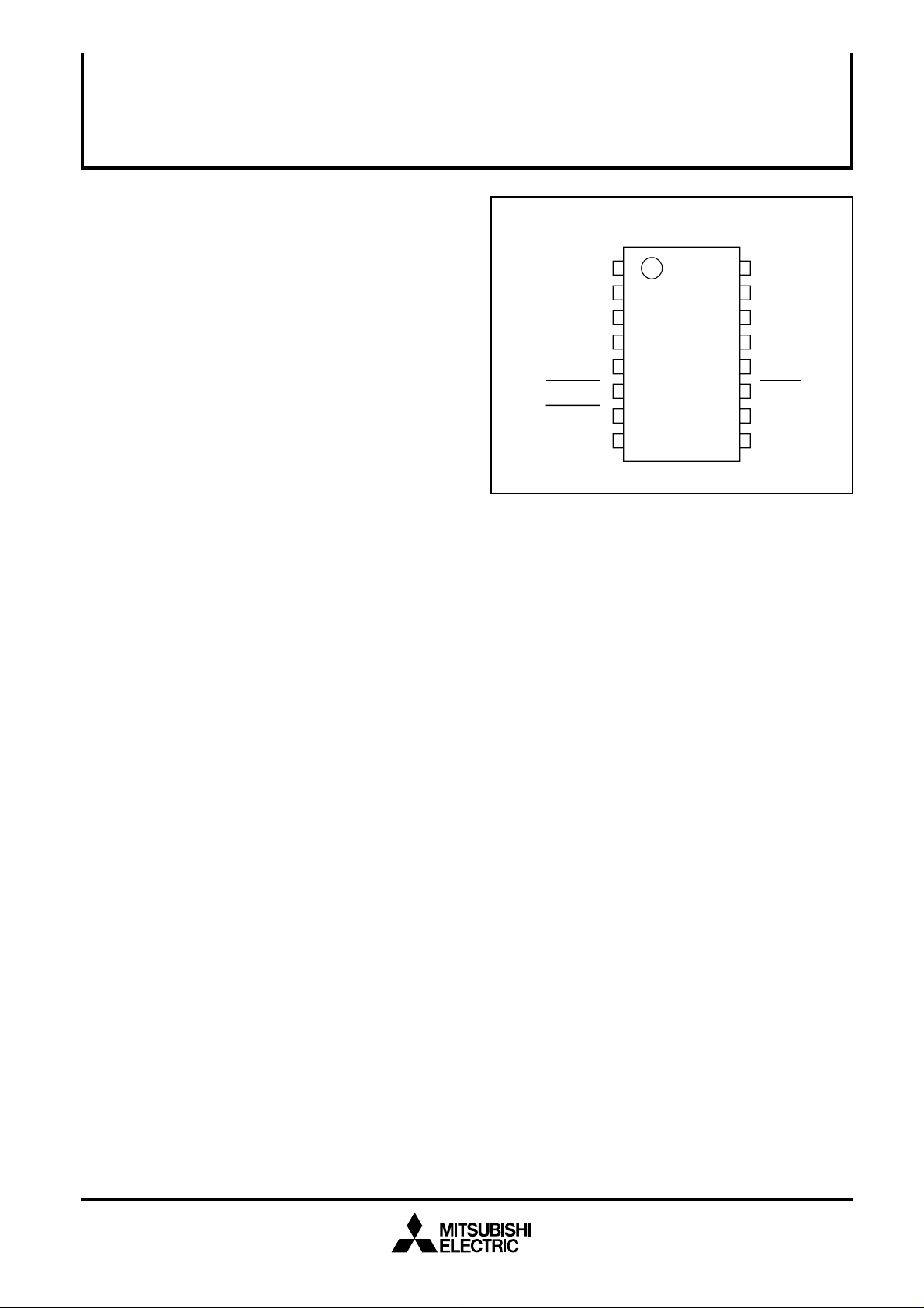
PIN CONFIGURATION (TOP VIEW)
The M64811AGP is a 1.1GHz/500MHz band two-system
one-chip PLL frequency synthesizer .
Using a high performance Bi-CMOS process , the product
contains one two-modulus (1/32 and 1/33) prescaler that
accepts inputs up to 1.1GHz and another two-modulus
(1/16 and 1/17) prescaler that accepts inputs up to
500MHz ,thus helping make the equipment compact .
FEATURES
• Operating supply voltage : 2.7V~3.6V
• Operating temperature : -30°C~+85°C
• 2 PLL systems (1.1GHz and 500MHz) are on one chip .
PLL1 : 700MHz~1.1GHz PLL2 : 100MHz~500MHz
• Low power consumption (Icc=8mA Typ at Vcc=3V) .
• Dividing ratio setting ranges :
FIN1 for 1.1GHz VCO• • • • • N(VCO1)=1,024~131,071
FIN2 for 500MHz VCO• • • • • N(VCO2)=256~131,071
OSC for Fref • • • • • • • • • • • • • N(Fref)=5~2,047
• Each loop has input pin for sleep mode .
Power supplies to 2 loops can be independently turned ON/OFF .
Also can be controlled by the serial data . (When SLEEP1 and SLEEP2 is "H" . )
• The PLL standard oscillation circuit can adopt a B-E Colpitts type oscillation circuit to from a stable
oscillation circuit.
• Current controlled charge pump . (Icp=±2mA const.)
• Locked condition detecting output
If a phase difference smaller than 3 times (∆t) of the OSC period continues for 15 periods or
longer , the condition is judged as locked, and the LOCK terminal goes to "L" .
(When , for example , fosc=19.2 MHz , ∆t=156 ns)
• PLL lock/unlock status indicate function .
(Judged in the system turned on if the other system is turned off . )
• Small package (16pin SSOP, lead pitch : 0.65mm)
FIN1
GND
CPS
LE
SLEEP1
SLEEP2
FIN2
SI
1
2
3
4
5
6
7
8
16
15
14
13
12
11
10
PD1
Vcc
XIN
XOUT
XBo
LOCK
GND
PD2
9
APPLICATION
• Digital cordless phone (CT2)
• Digital cellular phone (PDC)
1
1.1GHz/500MHz DUAL PLL FREQUENCY SYNTHESIZER FOR DIGITAL CELLULAR PHONE
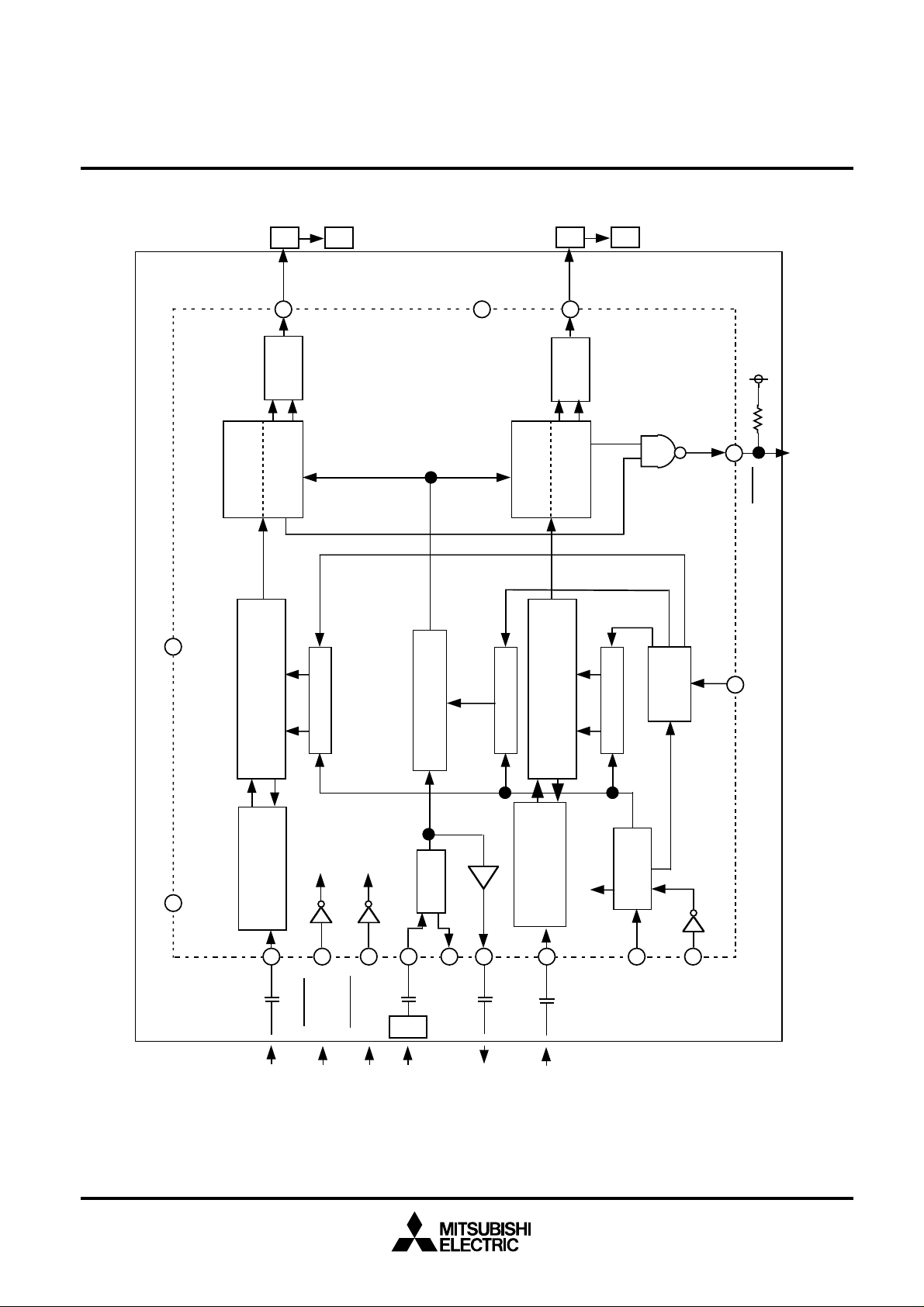
BLOCK DIAGRAM
LPF VCO
MITSUBISHI ICs (COMMUNICATION)
M64811AGP
LPF VCO
GND
PD2
9
CHARGE
PUMP
LOCK
PHASE
2
DETECTOR
DETECTOR
VCC
15
DATA LATCH
PROGRAMMABLE
SWALLOW / PROGRAMMABLE
COUNTER
REFERENCE COUNTER
PD1
16
CHARGE
LOCK
PHASE
DETECTOR
DATA LATCH
SWALLOW / PROGRAMMABLE
COUNTER
PUMP
DETECTOR
DATA LATCH
LATCH
SELECT
11
LOCK
5
LE
10
GND
ON/OFF
PLL1
(1/16, 1/17)
500MHz 2-MODULUS
PRESCALER
8
6
FIN2
SLEEP1
ON/OFF
PLL2
7
XIN
SLEEP2
TCXO
OSC
XOUT
131412
XBo
1.1GHz 2-MODULUS
PRESCALER
(1/32, 1/33)
SLEEP Control
1
FIN1
RESISTER
SHIFT
4
SI
3
CPS
2

1.1GHz/500MHz DUAL PLL FREQUENCY SYNTHESIZER FOR DIGITAL CELLULAR PHONE
FUNCTION DESCRIPTION OF PINS
MITSUBISHI ICs (COMMUNICATION)
M64811AGP
Pin No.
1
2
3
4
5
6
7
8
9
10
11
12
13
14
Pin Identification Description
FIN1
GND
CPS
SI Shift register data input pin
LE
SLEEP1
SLEEP2
FIN2
PD2
GND
LOCK
XBo
XOUT
XIN
Input from the VCO , Fmax = 1.1GHz .
Ground .
Clock pulse input .
Binary serial data input .
Load enable input . When LE is HIGH , data stored in the shift registers is loaded into the
appropriate latch .
PLL1 power control . "H" = normal operation , "L"=power down .
PLL2 power control . "H" = normal operation , "L"=power down .
Input from the VCO , Fmax = 500MHz .
Charge pump2 output . Tristate output . High Z when PLL2 power is off .
Ground .
When loops are locked ••••••••"L" , When one of loops is unlocked••••••••"High Z" .
If one loop is sleep mode , the status of the other loop is checked for judgment .
Buffer output of oscillator .
Crystal Oscillator input .
Shift register clock input pin .
15
16
Vcc
PD1
Power supply . Vcc = 2.7~3.6V .
Charge pump1 output . Tristate output . High Z when PLL1 power is off .
3

1.1GHz/500MHz DUAL PLL FREQUENCY SYNTHESIZER FOR DIGITAL CELLULAR PHONE
FUNCTION DESCRIPTION
1.Data Input
L E
S I
CPS
Invalid
MITSUBISHI ICs (COMMUNICATION)
M64811AGP
MSB
D1 D2 D19 D20 D21 D22
LSB
Note 1) At the leading edge of the CPS input , the status of the SI input is written into the shift
register .
Note 2) The bit just before LE becomes "H" is LSB , and SI before MSB becomes invalid .
Note 3) When LE is "H" , the data stored in the shift registers is loaded into the appropriate latch .
2.Input Signal Timing
L E
S I
tsu th
CPS
tsu=th=tWH=tWL=0.1µsmin.
tCR=tRH=0.1µsmin.
3.Bit Configuration of Shift Register
LSB
Shift register
Power on/off
setting
22 21 20 19 18 17 16 15 14 13 12 11 10 9 8 7 6 5 4 3 2 1
D
A DB DC
Valid data
tWH tWL
tCR
tRH
Data latch
setting
*
**
***
***
DD DE
HH
LH
HL
0
2
21222324252627282
Dividing ratio of reference counter
for reference frequency
4
202122232
Dividing ratio of
swallow counter
2021222
Dividing ratio of
swallow counter
3
0
2
21222324252627282
0
2
21222324252627282
MSB
10
9
2
Dividing ratio of programable counter
for local oscillator 1
Dividing ratio of programable counter
for local oscillator 2
Invalid
9
MSB
10
11
9
2
10
2
2112
2
MSB
Invalid
12
Invalid
4

MITSUBISHI ICs (COMMUNICATION)
1.1GHz/500MHz DUAL PLL FREQUENCY SYNTHESIZER FOR DIGITAL CELLULAR PHONE
Note 4) Power on/off control of PLL system is set by DA , DB , and DF .
M64811AGP
External Control Pin
SLEEP1 SLEEP2
L L * * * OFF OFF
L H 0 0 * OFF ON
L H 0 1 * OFF OFF ONON
L H 1 0 * OFF ON ONON
L H 1 1 * OFF OFF ONON
H L 0 0 * ON OFF ONON
H L 0 1 * ON OFF ONON
H L 1 0 * OFF OFF ONON
H L 1 1 * OFF OFF ONON
HH
HH
Serial Data
DA DB DC
111
110
Description
PLL1 PLL2
OFF OFF
OFF OFF
OSC
ON
ON
OFF
ON
XBo
ON
ON
OFF
ON
HH
HH
HH
HH
HH
HH
ON;Power on , OFF;Power off
101
100
011
010
001
000
OFF ON
OFF ON
ON OFF
ON OFF
ON ON
ON ON
Note 5) DD and DE are used to select latched data to be updated.
DD
Data
DE
0
0
10
01
Unused.
Data latched for local oscillator 1 is updated.
Data latched for local oscillator 2 is updated.
Description
ON
ON
ON
ON
ON
ON
OFF
ON
OFF
ON
OFF
ON
11
Data latched for reference frequency .
5

MITSUBISHI ICs (COMMUNICATION)
M64811AGP
1.1GHz/500MHz DUAL PLL FREQUENCY SYNTHESIZER FOR DIGITAL CELLULAR PHONE
Note 6) Dividing ratio of the reference counter for reference frequency is given by 11-bit binary coads .
N(fREF1)=5~2047
Note 7) Dividing ratio N(VCO1) of VCO1 for local oscillator1 is given by 5-bit swallow counter and 12-bit
Note 8) Dividing ratio N(VCO2) of VCO2 for local oscillator2 is given by 4-bit swallow counter and 13-bit
programable counter .
N(VCO1)=32 x M+A (A<M)
M : Preset dividing ratio of 12-bit programmable counter (32~4095)
A : Preset dividing ratio of 5-bit swallow counter (0~31)
programable counter .
N(VCO2)=16 x M+A (A<M)
M : Preset dividing ratio of 13-bit programmable counter (16~38191)
A : Preset dividing ratio of 4-bit swallow counter (0~315)
6

1.1GHz/500MHz DUAL PLL FREQUENCY SYNTHESIZER FOR DIGITAL CELLULAR PHONE
∫ ∫
∫ ∫
∫ ∫
4.Charge Pump and LOCK Detection
Reference frequency(Fref)
Divided output of
local oscillator (FVCO/N )
MITSUBISHI ICs (COMMUNICATION)
M64811AGP
Charge pump
output
"HiZ"
"Source"
"Sink"
123 15
LOCK output
Note 9) If the phase of divided local oscillator output (FVCO/N) is behind that of the reference
frequency (Fref) , the charge pump output becomes "Source" status , if advancing , "Sink" status .
Note 10) If a phase difference smaller than 3 times of the OSC period continues for 15 periods longer , the
LOCK output becomes "L" .
( When , for example , Fosc = 19.2 MHz , ∆t = 156 ns)
Note 11) If one of the power supplies to PLLs is turned off , a judgment is made based on only the condition
of the other loop .
Note 12) The LOCK output circuit yields an open drain N-channel transistor output . It should be pulled up to
Vcc .
5.Sleep Mode Input
By status of SLEEP1 and SLEEP2 , each PLL can be selected to either sleep mode ( Power supply is turned
off . ) or operation mode .
If SLEEP input is "H" , the PLL becomes normal operation mode .
( Power supplies to turn ON/OFF can be controlled by the serial data ; submit to note 4 . )
If SLEEP input is "L" , the PLL becomes sleep mode . ( Power supply is turned off . )
7

1.1GHz/500MHz DUAL PLL FREQUENCY SYNTHESIZER FOR DIGITAL CELLULAR PHONE
INPUT / OUTPUT CIRCUIT DIAGRAM
MITSUBISHI ICs (COMMUNICATION)
M64811AGP
12
SI,CPS<LE,SLEEP1,SLEEP2
Prescaler input(FIN1,FIN2)
V
CC
FIN
3
OSC input Charge Pump output(PD1,PD2)
4
VDD
XIN
XOUT
PD
XBo
5
LOCK
LOCK
8

MITSUBISHI ICs (COMMUNICATION)
M64811AGP
1.1GHz/500MHz DUAL PLL FREQUENCY SYNTHESIZER FOR DIGITAL CELLULAR PHONE
ABSOLUTE MAXIMUM RATINGS (Ta= -30~85°C, unless otherwise specified . )
Symbol Parameter Test Condition Unit
Vcc Supply Voltage
V
I
V
O Output Voltage Output pin : GND=0V
Pd Power Dissipation
Vopd Open Drain Voltage
Topr Operating Temperature
Tstg Storage Temperature -40 125
Input Voltage
GND=0V -0.3 4.5 V
SI , CPS , LE pin : GND=0V -0.3 4.5 V
Ta=85°C( Allowable dissipation of package )
GND=0V -0.3 4.5
RECOMMENDED OPERATING CONDITIONS (Ta= -30~85°C, unless otherwise specified . )
Symbol Parameter Test Condition Unit
Vcc Supply Voltage
FIN1
FIN2 100 500 MHz
VIN1
VIN2
VXIN 0.4 1.0 Vp-pVcc=2.7~3.6V
Operating Frequency
Input Sensitivity
Oscillator Sensitivity
@Recommendation : X'tal (19.2MHz)
Vcc=2.7~3.6V
FIN1=1.0~2.0GHz -10
FIN2=100~500MHz -16 -4
@
Min. Max.
Ratings
Min. Max.
-0.3 4.5 V
-30 85
Limits
Typ.
2.7 3.6
0.7 1.1 GHz
250 mW
°C
°C
2
dBm
V
V
ELECTRICAL CHARACTERISTICS (Ta= 25°C, unless otherwise specified . )
Symbol Parameter Test Condition Unit
I
I PD-
Charge Pump Output
PDSOURCE
(Source) Current
Charge Pump Output
SINK
(Sink) Current
Icc1
Icc2 mA
Icc3
Icc4
Supply Current
Pin
PD1 ,
PD2
Vcc
Vcc=3.0V ,
VPD=Vcc/2
Vcc=3V , Both PLLs are on .
Vcc=3V , Only PLL1 is on .
Vcc=3V , Only PLL2 is on .
Vcc=3V , Both PLLs are off .
Min. Max.
Limits
Typ.
2.0
-2.0
8.0
5.5
4.5
10
HANDLING PRECAUTIONS
1. This IC contains fine structure components to achieve high performance . Therefore , take extra
precaution to protect the IC from surge voltage caused by static electricity .
2. If one of two PLLs is not used , please make power supply of that turn off .
mA
µA
9
 Loading...