

Mitsubishi M64285K Datasheet

Technical Data Sheet
MITSUBISHI CMOS Image Sensor
MITSUBISHI
PRELIMINARY
M64285K
1. General Description
M64285K is a 32x32 pixel CMOS image sensor with the built-in image processor and the
analog conditioning function. It contains the information compressing and parallel
processing functions. It makes it possible to realize the image information input system to
become highly functional, smaller in size, faster in speed, and lower in power consumption.
2. Features
* Single 5.0V power supply.
* Low power dissipation (Typ. 15mW)
* Projection processing of two dimensional (2D) image to one dimensional (1D) image.
(Column and Row Projection)
* Outputting the average data of the overall image area
* Adjusting the gain, black level, and the data offset
* Variable data rate : 4φ ~ 64φ / pixel ( φ is the clock cycle time )
* It is possible to use 8 bit microcontroller for controlling purposes.
3. Application
Image inputting systems for gaming devices, interface systems, security, surveillance,
factory automation, etc.
( 1 / 26 )
Specifications and information herein are subject to change without notice.
02 / 05 / 01
Ver. 1.1E_01

Technical Data Sheet
Pin
AVDD1
AVDD2
AGND2
AGND1
MITSUBISHI
PRELIMINARY
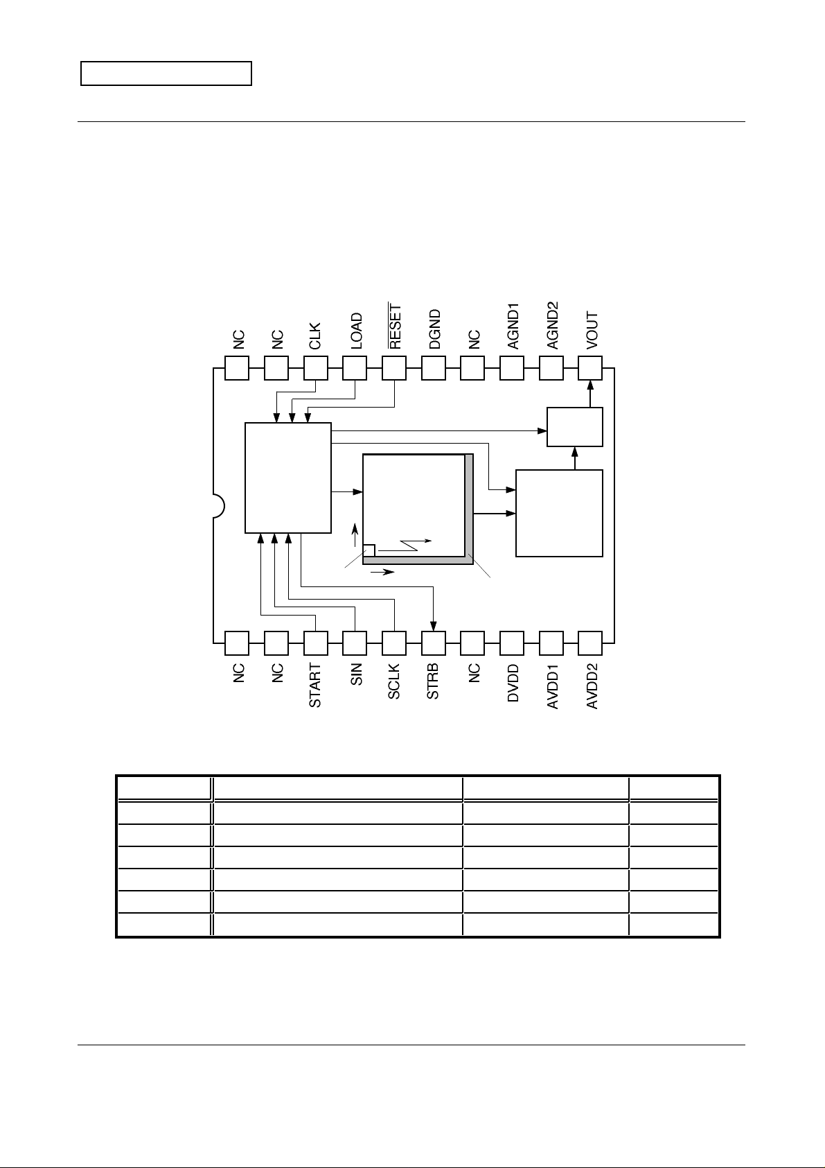
4. Pin Configuration ( Top View )
Pixel Origin
MITSUBISHI CMOS Image Sensor
M64285K
11121314151617181920
1 2 3 4 5 6 7 8 9 10
Pin No.
1 NC
2 NC
3 START Counter RESET, Image capture start Digital input
4 SIN Register setting data Digital input
5 SCLK Register data input timing Digital input
6 STRB Data output timing Digital output
7 NC
8 DVDD Digital Power supply Power supply
9
10
11 VOUT Voltage output of image data Analog output
12
13
14 NC
15 DGND Digital GROUND GROUND
Outline of functions Pin types
Pixel & Analog Power supply Power supply
AMP Power supply Power supply
AMP GROUND GROUND
Pixel & Analog GROUND GROUND
Outline : 20K2X-A ( 20 pin SOP )
16 RESET Chip RESET (LOW active) Digital input
17 LOAD Register data input trigger Digital input
18 CLK System clock Digital input
19 NC
20 NC
* Digital pins use CMOS input and CMOS output.
* The potential of digital pins must normally be fixed to "H" or "L".
( 2 / 26 )
Specifications and information herein are subject to change without notice.
02 / 05 / 01
Ver. 1.1E_01
Technical Data Sheet
Elimination
MITSUBISHI
PRELIMINARY
5. Structure and Block Diagram of the Device
Effective pixels 32 x 32
Total pixels 33 x 33
Image area 1.79 mm x 1.79 mm (1/6 inch, optical system)
Pixel size 56 µm x 56 µm
Optical black Horizontal direction (H):1 pixel behind
Vertical direction (V):1 pixel before
18 17 16 15 14
1920 13 12 11
MITSUBISHI CMOS Image Sensor
M64285K
AMP
Register
Sequencer
Pixel Origin
3 4 5 6 7
21 8 9 10
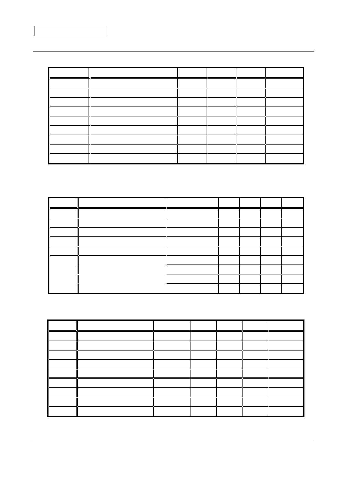
6. Absolute Maximum Ratings
Symbols Items Ratings Units
DVDD Digital Power supply 6 V
AVDD1 Pixel & Analog Power supply 6 V
AVDD2 AMP Power supply 6 V
VI
Topt Operating ambient temperature -10 ~ +60 °C
Tstg Storage temperature -20 ~ +80 °C
Digital input voltage * -0.3 ~ VDD V
Pixel Array
V
Scan Direction
32 x 32
H
Analog
Processing
Noise
Optical Black
Pixels
* Digital input terminals : START, SIN, SCLK, RESET, LOAD, and CLK
( 3 / 26 )
Specifications and information herein are subject to change without notice.
02 / 05 / 01
Ver. 1.1E_01
Technical Data Sheet
MITSUBISHI
PRELIMINARY
7. Recommended Operating Conditions
Symbols Items Min. Typ. Max. Units
Topt Operating ambient temperature 0 25 45 °C
DVDD Power supply 4.5 5 5.5 V
AVDD1 Power supply 4.5 5 5.5 V
AVDD2 Power supply 4.5 5 5.5 V
VIH
VIL
f clk
f sclk
** Light source: Uniform light from a 2856 ± 150 K halogen light valve without IR cut filter.
"H" Digital input voltage * 0.8 DVDD DVDD V
"L" Digital input voltage * 0 0.6 V
System clock 0.5 2 MHz
Register input clock 0.5 2 MHz
Faceplate Illumination ** 0.5 500 lx
* Digital input terminals : START, SIN, SCLK, RESET, LOAD, and CLK
MITSUBISHI CMOS Image Sensor
M64285K
8. DC Electrical Characteristics
Symbols Items Conditions Min. Typ. Max. Units
VOH
VOL
Iout
RO
DIDD
AIDD
"H" digital output voltage * IOH = -2 mA 4.5 5 V
"L" digital output voltage * IOL = +2 mA 0 0.5 V
Analog output current capability ** -200 200 µA
Analog output resistance ** Iout = ±200 µA 75
Digital circuit current ** 0.6 mA
Analog circuit currents 2D image (peak) 4 mA
( Accum. time = 10 ms ) 2D image (ave.) 1.7 mA
( Power Save = on ) Proj. image (peak) 4 mA
* Digital output terminal: STRB ** Analog output terminal: VOUT
9. Electrical and Optical Characteristics
Symbols Items Conditions Min. Typ. Max. Units
Range of accumulation time Clk = 2 MHz 16 µ 1 sec
Range of data rate Clk = 2 MHz 2 32 µs / pixel
Read out time ( 2D image ) Clk = 2 MHz 2.74 34.4 ms
Read out time ( proj. image ) Clk = 2 MHz 0.26 2.18 ms
Black level output setting 1 2 V
S Sensitivity * Gain = 0 dB 20 V / lx • s
Vsat Saturation output voltage Gain = 0 dB 2000 mV
Vo Average standard output Gain = 0 dB 1000 mV
Vdrk Dark signal Gain = 0 dB 0.1 V / s
( VDD = 5.0V, Ta = 25 °C )
Ω
Proj. image (ave.) 0.9 mA
( VDD = 5.0V, Ta = 25 °C )
* Light source: Uniform light from a 2856 ± 150 K halogen light valve without IR cut filter.
( 4 / 26 )
Specifications and information herein are subject to change without notice.
02 / 05 / 01
Ver. 1.1E_01
Technical Data Sheet
MITSUBISHI
PRELIMINARY
MITSUBISHI CMOS Image Sensor
M64285K
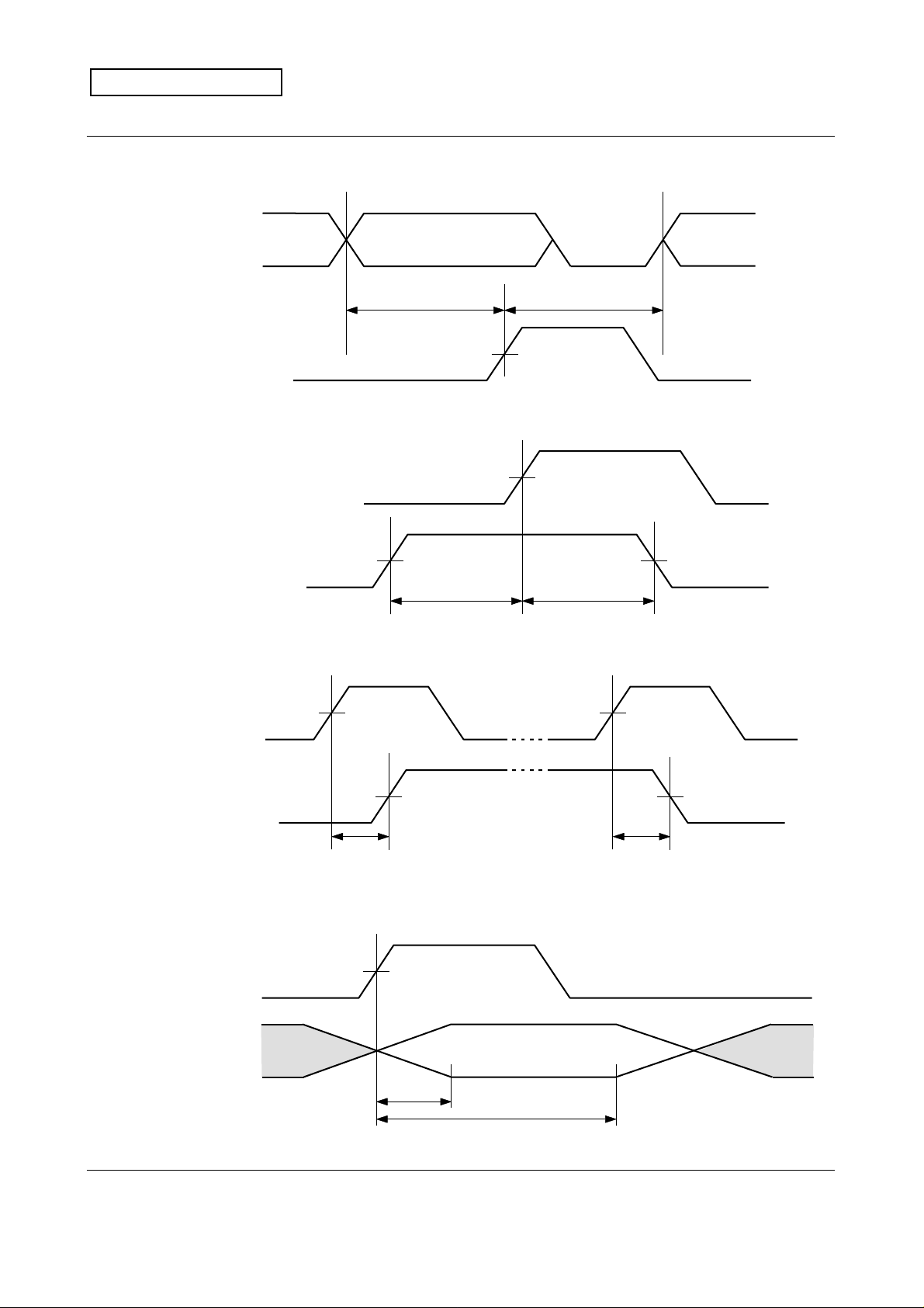
10. Electrical Characteristics (AC)
Symbols Items Min. Typ. Max. Units
tc (CLK)
tWH (CLK)
tWL (CLK)
tr (CLK)
tf (CLK)
tc (SCLK)
tWH (SCLK)
tWL (SCLK)
tr (SCLK)
tf (SCLK)
tWL (RESET)
tD (RESET-SIN)
tS (SIN)
tH (SIN)
tD (SIN-LOAD)
tD (LOAD-SIN)
tS (LOAD)
tH (LOAD)
tS (START)
tH (START)
tDR (CLK_STRB)
tDF (CLK_STRB)
tr (VOUT)
tH (VOUT)
RESET pulse width ( "L" level ) 200 - - ns
CLK-STRB delay time (Rise) ** - - 100 ns
CLK cycle time * 0.5 0.5 2 µs
CLK pulse width ( "H" level ) 240 - - ns
CLK pulse width ( "L" level ) 240 - - ns
CLK rise time - - 10 ns
CLK fall time - - 10 ns
SCLK cycle time 0.5 - - µs
SCLK pulse width ( "H" level ) 240 - - ns
SCLK pulse width ( "L" level ) 240 - - ns
SCLK rise time - - 10 ns
SCLK fall time - - 10 ns
RESET-SIN delay time 100 - - ns
SIN setup time 50 - - ns
SIN hold time 50 - - ns
SIN-LOAD delay time ( Note 1 ) - - ns
LOAD-SIN delay time ( Note 2 ) - - ns
LOAD setup time 50 - - ns
LOAD hold time 50 - - ns
START setup time 50 - - ns
START hold time 50 - - ns
CLK-STRB delay time (Fall) ** - - 100 ns
VOUT stabilization time ** - 600 - ns
VOUT hold time - - ( Note 3 ) µs
( Ta = 25 °C )
* Hereafter CLK cycle time is written to be φ.
** Load Capacitance = 50 pF
Specifications and information herein are subject to change without notice.
( 5 / 26 )
Note 1: tD (SIN-LOAD) ≥ 100 + tS (SIN) - tS (LOAD)
Note 2: tD (LOAD-SIN) ≥ 100 + tS (LOAD) - tS (SIN)
Note 3: tH (VOUT) ≤ ( DOC - φ / 2 ) x tC (CLK) - 0.1 [µs]
DOC: see the explanation of DR register.
02 / 05 / 01
Ver. 1.1E_01
Technical Data Sheet
MITSUBISHI
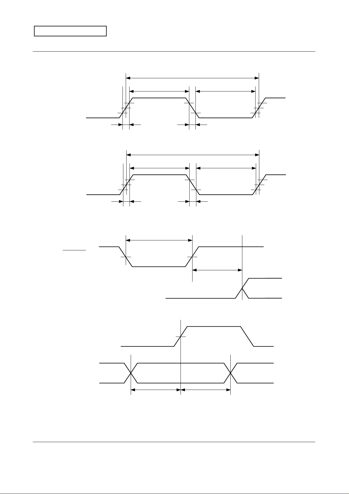
(A) CLK Timing
PRELIMINARY
tc (CLK)
tWH (CLK) tWL (CLK)
MITSUBISHI CMOS Image Sensor
M64285K
CLK
(B) SCLK Timing
SCLK
(C) RESET Timing
RESET
25%
25%
75%
75%
tr (CLK) t f (CLK)
tc (SCLK)
tWH (SCLK) t WL (SCLK)
tr (SCLK)
tf (SCLK)
tWL (RESET)
tD (RESET-SIN)
SIN
(D) SCLK, SIN Timing
SCLK
SIN
Specifications and information herein are subject to change without notice.
tS (SIN) tH (SIN)
( 6 / 26 )
A3
02 / 05 / 01
Ver. 1.1E_01
Technical Data Sheet
MITSUBISHI
(E) SIN, LOAD Timing
PRELIMINARY
LSB MSB
MITSUBISHI CMOS Image Sensor
M64285K
SIN
tD (SIN-LOAD)
LOAD
(F) CLK, LOAD, & START Timing
CLK
LOAD, START
(G) CLK, STRB Timing
D0D1 A3
tD (LOAD-SIN)
tS (LOAD) tH (LOAD)
tS (START) tH (START)
CLK
STRB
tDR (CLK-STRB) tDF (CLK-STRB)
(H) STRB, VOUT Timing
STRB
VOUT
Data
tr (VOUT)
tH (VOUT)
( 7 / 26 )
Specifications and information herein are subject to change without notice.
02 / 05 / 01
Ver. 1.1E_01
Technical Data Sheet
MITSUBISHI
11. Description of Functions
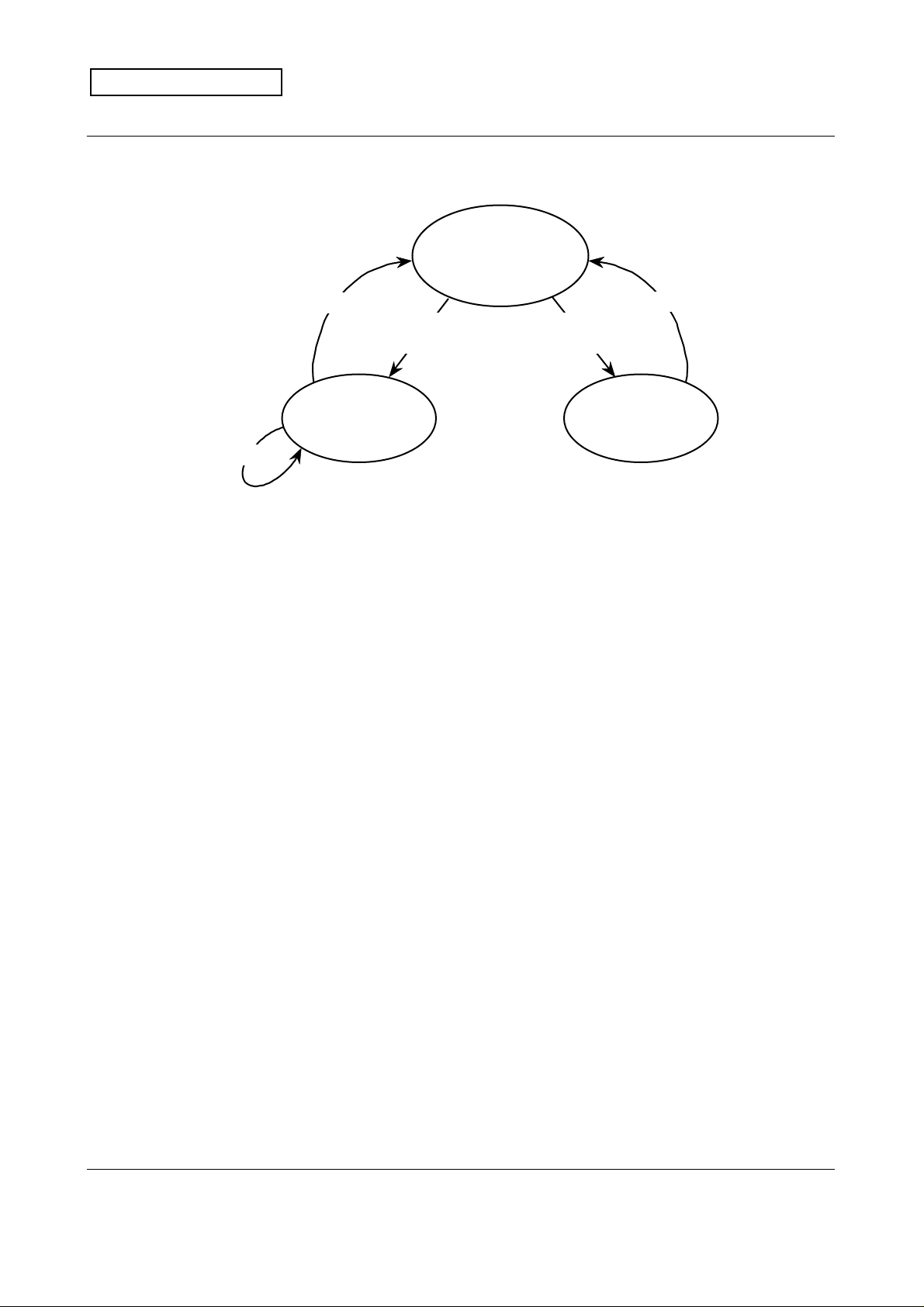
11.1. State Diagram
Set STOP=1
PRELIMINARY
Standby
• Register setting
• Reset State
Assert START
(MD3=0)
Assert START
MITSUBISHI CMOS Image Sensor
M64285K
Image output over
(MD3=1)
Continuous Mode
image capture
& output
Assert START
Snapshot Mode
image capture
& output
The state diagram of M64285K is shown above. The sequence to control M64285K is
explained below.
(1) Reset all the registers and counters.
RESET is set to "L" (asynchronous to CLK). Reset state is in the Standby state.
(2) Set the contents of the registers.
There are 16 sets of registers, consisting of 4 bits each. The input data is composed of 8
bits. The leading 4 bits are for address and the following 4 bits are for data. The input
data is latched at the rising edge of SCLK. When LOAD goes "H", the contents of the
register become fixed at the rising edge of CLK.
(3) Start image capture.
After the contents of all the registers are fixed, START is asserted in synchronous with
the rising edge of CLK. Then the control counters are reset to the initial value specified
by the registers, and the image capture sequence starts. After the accumulation time
defined by the registers 4 ~ 7, the analog image signals are outputted serially. The STRB
pulse is outputted in synchronous with the above. The number of active data on one
frame is 1024 for the 2D image, 64 for the projection image, and 1 for the pixel average
data; the number of data outputted in each modes is fixed by the combination of the
above. When this chip finishes outputting the defined number of data, in the snapshot
modes (MD3=1), it automatically falls into the Standby state. In the continuous modes
(MD3=0), once the image capture sequence starts, this chip carries on outputting the
image data, unless START is asserted again or STOP bit is set to "H" to force the chip
into the Standby state.
The contents of the registers can be changed in the Standby state. When START is asserted
in the standby state or in the continuous image capture sequence, the control counters are,
again, reset to the initial value specified by the registers, and the image capture sequence
starts. If the register contents are changed before asserting START, M64285K outputs the
data in a different mode. In the continuous output modes, register No. 2 including the STOP
bit is the only register that is allowed to be set.
( 8 / 26 )
Specifications and information herein are subject to change without notice.
02 / 05 / 01
Ver. 1.1E_01
 Loading...