


PRELIMINARY
Notice: This is not a final specification.
Some param
its are subject to change.
etric lim
MITSUBISHI SEMICONDUCTOR <TRANSISTOR ARRAY>
M63850P/FP
4-UNIT 1.5A DMOS ARRAY WITH CLAMP DIODE
DESCRIPTION
The M63850P/FP is a inverter input power DMOS transistor
array that consists of 4 independent output N-channel
DMOS transistors.
FEATURES
4 circuits of N-channels DMOS
High breakdown voltage (V
High-current driving (I
DS ≥ 80V)
DS(max) = 1.5A)
With clamping diodes
Drain-source on-state low resistance
(R
ON = 0.72Ω, @ = 1.25A)
Wide operating temperature range (Ta = –40 to +85°C)
APPLICATION
Drives of relays and printers, digit drives of indication elements (LEDs and lamps)
PIN CONFIGURATION
1
COM →O4
2
O1←
IN1→
3
4
GND
5
IN2→
6
NC
7
8
O2← COM
Package type
CIRCUIT DIAGRAM
30k
INPUT
4.2k
16
15
14
13
12
11
10
9
16P4(P)
16P2N(FP)
V
DD
←IN4
V
DD
GND
←IN3
→O3
NC : No connection
COM
OUTPUT
FUNCTION
The M63850P/FP is consists of 4 independent N-channel
DMOS transistors. Each DMOS transistor is connected in a
common-source with GND PIN. The clamp diodes for spike
killers are connected between the output pin and the COM
pin of each DMOS transistor. The maximum of Drain current
is 1.5A. The maximum Drain-Source voltage is 80V.
ABSOLUTE MAXIMUM RATINGS (Unless otherwise noted, Ta = –40 ~ +85°C)
DD
V
VDS
IDS
VI
VR
IF
Pd
Topr
Tstg
Supply voltage
Drain-source voltage
Drain current
Input voltage
Clamping diode reverse voltage
Clamping diode forward current
Power dissipation
Operating temperature
Storage temperature
Output, H
Current per circuit output, L
Ta = 25°C, when mounted on board
GND
The four circuits share the COM and GND.
The diode, indicated with the dotted line, is parasitic, and
cannot be used.
Unit : Ω
Ratings
7
–0.5 ~ +80
1.5
–0.5 ~ VDD
80
1.5
1.47(P)/1.00(FP)
–40 ~ +85
–55 ~ +125
UnitSymbol Parameter Conditions
V
V
A
V
V
A
W
°C
°C
Apr. 2005
MITSUBISHI SEMICONDUCTOR <TRANSISTOR ARRAY>
PRELIMINARY
Notice: This is not a final specification.
Some param
RECOMMENDED OPERATING CONDITIONS (Unless otherwise noted, Ta = –40 ~ +85°C)
Symbol
VDD
VDS
DS
I
VIH
VIL
ELECTRICAL CHARACTERISTICS (Unless otherwise noted, Ta = 25°C)
Symbol UnitParameter Test conditions
DD(ON)
I
IDD(OFF)
IO(LEAK)
VON
RON
IIH
IIL
IR
VF
its are subject to change.
etric lim
Parameter
Supply voltage
Drain-source voltage
Drain current
(Current per 1 circuit when 4
circuits are coming on simultaneously)
“H” input voltage
“L” input voltage
On supply current
Off supply current
Output leak current
Output on voltage
on resistance
Output
“H” input current
“L” input current
Clamping diode reverse current
Clamping diode forward voltage
Conditions
VDD = 5V, Duty Cycle
P : no more than 4%
FP : no more than 2%
V
DD = 5V, Duty Cycle
P : no more than 36%
FP : no more than 15%
VDD = 5.5V, VI = 0V, 1 circuit only
DD = 5.5V, VI = 5.5V
V
DD = 5.5V, VI = 5.5V, VDS = 80V
V
I = 4.5V, IDS = 0.7A
V
I = 4.5V, IDS = 1.25A
V
I = 4.5V, IDS = 1.25A
V
DD = 5.5V, VI = 5.5V
V
DD = 5.5V, VI = 0V
V
R = 80V
V
F = 1.25A
I
4-UNIT 1.5A DMOS ARRAY WITH CLAMP DIODE
M63850P/FP
Limits
min typ max
4.5
V
CC-1.0
min typ max
—
—
—
—
—
—
—
—
—
—
5.0
—
0
0
—
0
—
—
—
0
Limits
130
—
—
0.45
0.9
0.72
—
–130
—
1.3
5.5
80
1.25
0.7
CC
V
VCC-3.0
300
10
10
0.72
1.44
1.15
10
–300
10
2.0
Unit
V
V
A
V
V
µA
µA
µA
V
Ω
µA
µA
µA
V
SWITCHING CHARACTERISTICS (Unless otherwise noted, Ta = 25°C)
Symbol UnitParameter Test conditions
t
on
toff
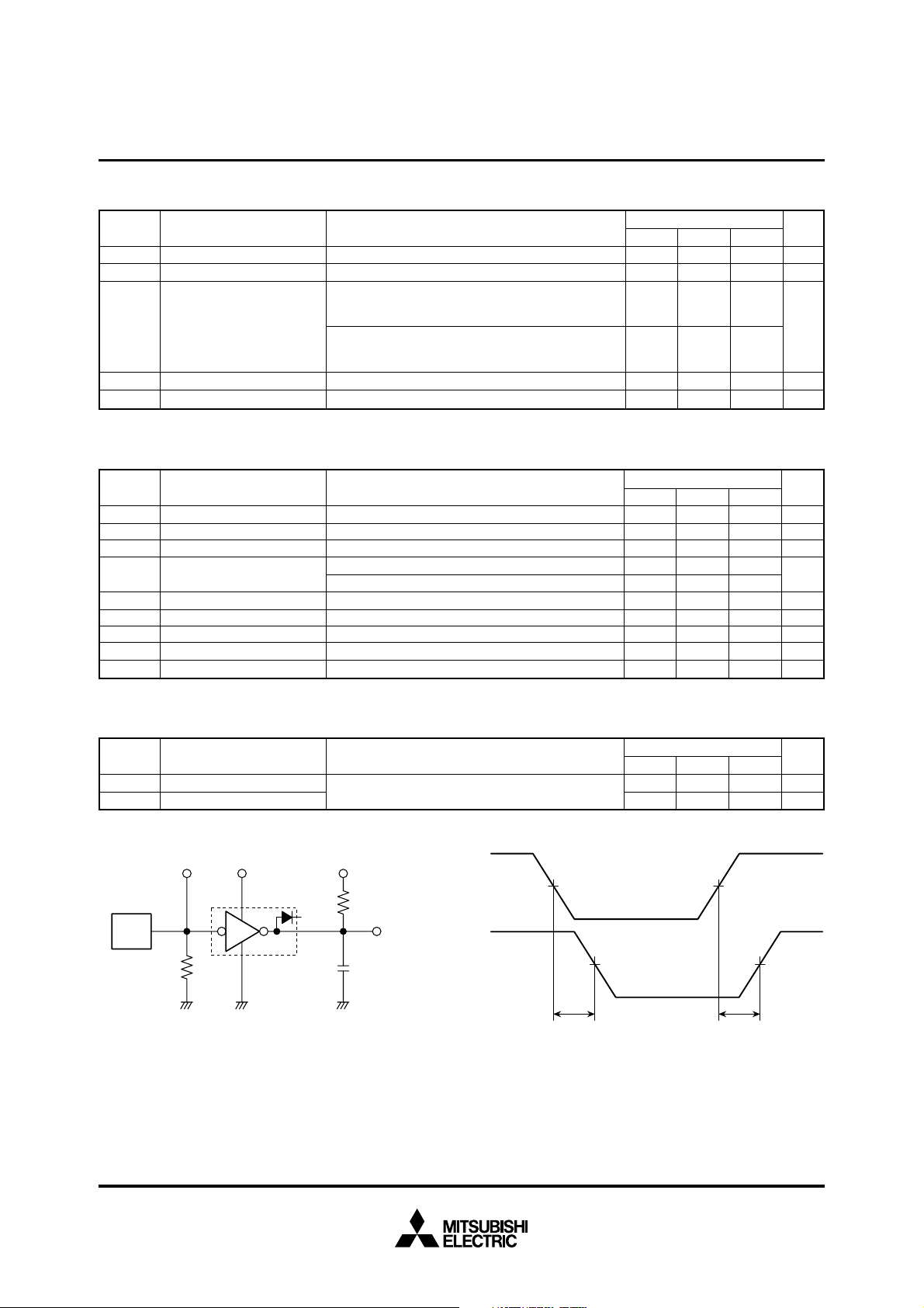
Note 1 : TEST CIRCUIT
Turn-on time
Turn-off time
INPUT VDD
Measured
device
PG
50Ω
(1)Pulse generator (PG) characteristics : PRR = 1kHz,
tw = 10µs, tr = 6ns, tf = 6ns, Zo = 50Ω, V
(2)Input-output conditions : R
(3)Electrostatic capacity C
at connections and input capacitance at probes.
OPEN
L = 8.3Ω, Vo = 10V, VDD = 4.5V
L includes floating capacitance
CL = 15pF (Note 1)
V
O
RL
OUTPUT
L
C
IH = 5V
TIMING DIAGRAM
min typ max
—
—
INPUT
50% 50%
OUTPUT
50% 50%
t
on
Limits
45
125
—
—
t
off
ns
ns
Apr. 2005

PRELIMINARY
Notice: This is not a final specification.
Some param
its are subject to change.
etric lim
TYPICAL CHARACTERISTICS
MITSUBISHI SEMICONDUCTOR <TRANSISTOR ARRAY>
M63850P/FP
4-UNIT 1.5A DMOS ARRAY WITH CLAMP DIODE
Thermal Derating Factor Characteristics
2.0
M63850P
1.5
(W)
d
M63850FP
1.0
0.5
Power dissipation P
0
0 255075100
85
Ambient temperature Ta (°C)
Duty Cycle - Drain Current Characteristics
(M63850P)
2.0
1.5
(A)
DS
1.0
•The drain current values represent the
Drain current I
0.5
current per circuit.
•Repeated frequency ≥ 10Hz
•The value in the circle represents the value of the
simultaneously-operated circuit.
•Ta = 25°C, V
0
0 20406080100
DD
= 5V
0.744
0.520
Input Characteristics
–160
VDD = 5V
–120
(µA)
I
–80
Ta = 85°C
Input current I
–40
Ta = –40°C
0
012345
Ta = 25°C
Input voltage V
DD - VI (V)
Duty Cycle - Drain Current Characteristics
(M63850P)
2.0
1.5
(A)
1
DS
•The drain current values
represent the current per circuit.
•Repeated frequency ≥ 10Hz
•The value in the circle represents
the value of the simultaneouslyoperated circuit.
•Ta = 85°C, V
DD
= 5V
1.0
2
3
4
Drain current I
0.5
0
0 20406080100
1
2
3
4
Duty cycle (%) Duty cycle (%)
Duty Cycle - Drain Current Characteristics
(M63850FP)
(A)
DS
2.0
1.5
•The drain current values
represent the current per circuit.
•Repeated frequency ≥ 10Hz
•The value in the circle represents
the value of the simultaneouslyoperated circuit.
•Ta = 25°C, V
DD
= 5V
1.0
Drain current I
0.5
0
0 20406080100
Duty cycle (%)
Duty Cycle - Drain Current Characteristics
2.0
1.5
(A)
DS
(M63850FP)
•The drain current values
represent the current per circuit.
•Repeated frequency ≥ 10Hz
•The value in the circle represents
the value of the simultaneouslyoperated circuit.
•Ta = 85°C, V
DD
= 5V
1.0
1
2
3
4
0.5
Drain current I
0
0 20406080100
1
2
3
4
Duty cycle (%)
Apr. 2005

PRELIMINARY
Notice: This is not a final specification.
Some param
its are subject to change.
etric lim
MITSUBISHI SEMICONDUCTOR <TRANSISTOR ARRAY>
M63850P/FP
4-UNIT 1.5A DMOS ARRAY WITH CLAMP DIODE
Input Voltage - Drain Current
1.6
V
DD
DS
V
1.2
(A)
DS
0.8
Drain current I
0.4
0
012345 012345
Characteristics
= 5V
= 2V
Ta = –40°C
Input voltage V
Ta = 25°C
I
(V)
Ta = 85°C
Output On Voltage - Drain Current
1.6
DD
V
I
= 0.5V
V
1.2
(A)
DS
Ta = –40°C
0.8
Drain current I
0.4
Characteristics
= 4.5V
Ta = 85°C
Ta = 25°C
Supply Voltage - On Supply Current
160
(µA)
120
DD(ON)
V
I
= 0.5V
One circuit only
Characteristics
80
Ta = 85°C
40
On-state supply current I
0
Supply voltage VDD (V)
Output On Voltage - Drain Current
Characteristics
= 4.5V
(A)
DS
200
160
120
V
DD
I
= 0.5V
V
Ta = –40°C
80
Drain current I
40
Ta = –40°C
Ta = 25°C
Ta = 85°C
Ta = 25°C
0
0
0.4 0.8 1.2 1.6
Output on voltage V
Clamping Diode Characteristics
1.6
(A)
F
1.2
0.8
Ta = 85°C
Ta = 25°C
0.4
Clamping diode forward current I
0
0
0.4 0.8 1.2 1.6
Clamping diode forward voltage V
ON
(V)
Ta = –40°C
F
(V)
0
0
0.05 0.10 0.15 0.20
Output on voltage V
Switching Characteristics
3
10
Ta = 25°C
7
5
3
2
2
10
7
5
Switching time (nsec)
3
2
1
10
1
23 57 23 57
10
Drain current I
10
off
t
t
on
2
23 57
DS
ON
3
10
(mA)
(V)
10
4
Apr. 2005

PRELIMINARY
Notice: This is not a final specification.
Some param
its are subject to change.
etric lim
MITSUBISHI SEMICONDUCTOR <TRANSISTOR ARRAY>
M63850P/FP
4-UNIT 1.5A DMOS ARRAY WITH CLAMP DIODE
Drain Current - Output On Resistance
1.0
Ta = 25°CV
(Ω)
ON
0.8
Characteristics
Vcc = 4.5V
Vcc = 5.0V
Output On Resistance - Ambient Temperature
Characteristics
= 4.5V
(Ω)
ON
1.6
DD
1.2
0.6
0.8
0.4
0.2
0
Drain-source on-state resistance R
1
23 57 23 57 23 57
10
10
2
Drain current IDS (mA)
Vcc = 5.5V
3
10
10
0.4
0
0
0
4
Drain-source on-state resistance R
–40 –20 0 20 40 10060 80
Ambient temperature Ta (°C)
Apr. 2005
 Loading...