


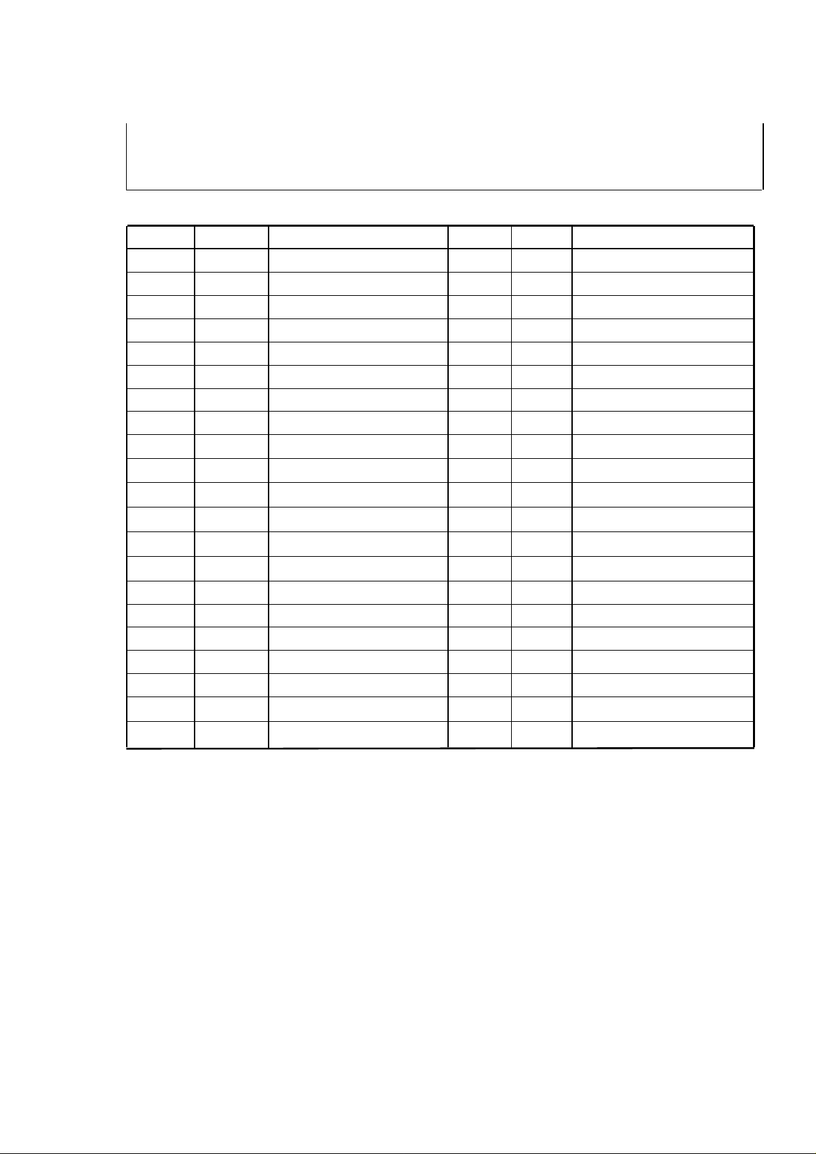
M63020FP
( / 17)
MITSUBISHI SEMICONDUCTORS
REV990726
[ Features ]
[ APPLICATION ]
CD-ROM, DVD, DVD-ROM, DVD-RAM ,Optical disc related system,etc
1
LOIN+
TO+
TO-
GND
SPIN
FG
Detect
comp.
Logic
Hall Bias
BIAS
TSD
Regulator
Logic
s
comp.
comp.
SPINDLE MOTOR AND 5CH ACTUATOR DRIVER
This IC is 1 chip driver IC for spindle motor and 5 channel
actuators. All of the motor and actuator of optical disk drive
system (CD-ROM etc.) can be drived by only this IC.
This IC has a direct PWM control system for Spindle and Slide
channels drive due to reducing IC power dissipation.
This IC has three voltage supply terminals (for Spindle,
Slide,Focus/Tracking and Loading) , and three voltage
supply can be set separately.
Further more this IC has short braking select function,FG
amplifier, thermal shut down circuit, standby circuit, reverse
rotation detect circuit.
(Top View)
SL1IN
SL2IN
VM2
RSL2
SL2+
SL2-
GND
RSL1
SL1+
SL1-
GND
W
V
U
RSP
Hw-
Hw+
HvHv+
HuHu+
PIN CONFIGURATION
1
2
3
4
5
6
7
8
9
10
11
12
13
14
15
16
17
18
19
20
21
Package outline : 42 PIN POWER SSOP (42P9R-B)
42
OSC
41
MU1
40
LOIN-
39
38
BRS
LO-
37
36
LO+
35
FO-
34
FO+
33
GND
32
31
5VCC
30
29
28
TOIN
27
FOIN
26
25
REF
24
FG
23
HB
22
VM1
[ BLOCK DIAGRAM ]
FG
HU+
HUHV+
HVHW+
HWHB
SPIN
REF
SL1IN
SL2IN
FOIN
TOIN
CTL
amp.
Reverse
MATRIX
Direction
comp.
s s s
120∫
Current
CTL
amp.
Direction
comp.
X5
Current
comp.
X5
CTL
amp.
Direction
Current
Frequency
generator
5V power supply
X5
MU1
OSC
M63020FP
( / 17)
MITSUBISHI SEMICONDUCTORS
REV990726
2
[ PIN FUNCTION ]
SPINDLE MOTOR AND 5CH ACTUATOR DRIVER
TERMINAL
1
2
3
4
5
6
7
8
9
10
11
12
13
14
15
16
17
18
19
20
21
SYMBOL
SL1IN
SL2IN
VM2
RSL2
SL2+
SL2-
GND
RSL1
SL1+
SL1-
GND
W
V
U
RSP
HW-
HW+
HV-
HV+
HU-
HU+
TERMINAL FUNCTION
Slide control voltage input 1
Slide control voltage input 2
Motor Power Suppry 3 (for Slide)
Slide current sense 2
Slide non-inverted output 2
Slide inverted output 2
GND
Slide current sense 1
Slide non-inverted output 1
Slide inverted output 1
GND
Motor drive output W
Motor drive output V
Motor drive output U
Spindle current sensie
HW- sensor amp. input
HW+ sensor amp. input
HV- sensor amp. input
HV+ sensor amp. input
HU- sensor amp. input
HU+ sensor amp. input
TERMINAL TERMINAL FUNCTION
42
41
40
39
38
37
36
35
34
33
32
31
30
29
28
27
26
25
24
23
22
SYMBOL
OSC
MU1
LOINLOIN+
BRS
LOLO+
FOFO+
GND
TO+
TO-
5VCC
GND GND
TOIN
FOIN
SPIN
REF
FG
HB
VM1
PWM carrier oscilation set
mute 1
Loading control input(-)
Loading control input(+)
Brake select control terminal
Loading inverted output
Loading non-inverted output
Focus inverted output
Focus non-inverted output
GND
Tracking non-inverted output
Tracking inverted output
5V Power Supply (for FS ,TS,LO)
Tracking control voltage input
Focus control voltage input
Spindle control voltage input
Reference voltage input
Frequency generator output
Bias for Hall Sensor
Motor Power Suppry 1 (for Spindle)

M63020FP
( / 17)
REV990726
3
-20 to +75
-40 to +150
VM2
IoA
Vin
PtTjTopr
Tstg
150
W
Storage temperature
0 to 5VCC
V
[ABSOLUTE MAXIMUM RATING] (Ta=25ºC)
1.0
20.8
2.6
15
15VVM1
5VCC
7VIoB
1.2
VV12
[RECOMMENDED OPERATING CONDITIONS] (Ta=25ºC)
minimum
typical
maximum
Unit
VM1
13.2
A
KHz
A
0.5
0.5V12
VM2
4.5
13.2
6
1.0
0.8
120
30
574.5
when it is used above 0.6A. Discription(IoA) is case of with external shottky diode.
MITSUBISHI SEMICONDUCTORS
SPINDLE MOTOR AND 5CH ACTUATOR DRIVER
SYMBOL
Kθ mW / ºC
*note1 ; The ICs must be operated within the Pt (power dissipation) or the area of safety operation
PARAMETER CONDITIONS
5V power supply
Motor power supply 1
Motor power supply 2
Motor Output Current A
Motor Output Current B
Maximum input voltage
of terminals
Power dissipation
Thermal derating
Junction temperature
Operating temperature
Focus,Tracking and Loading power supply
Spindle power supply
Slide power supply
Focus,Tracking and Loading output current
Spindle and Slide output current
MU1,Hw-,Hw+,Hv,Hv+,Hu-,Hu+,REF,SPIN,BRS
TOIN,FOIN,OSC,SLIN1,SLIN2,LOIN-,LOIN+
Free Air and on the grass epoxy board
Free Air and on the grass epoxy board
*note 1
RATING
Unit
V
A
A
ºC
ºC
ºC
The spindle and slide output terminal is needed external shottky diode between each output and GND
when it is used above 0.6A. Discription(IoA) is case of with external shottky diode.
LIMITS
SYMBOL PARAMETER
VM1 power supply(for Spindle)
VM2 power supply(for Slide)
5VCC
IoA
IoB
Fosc
*note2
The spindle and slide output terminal is needed external shottky diode between each output and GND
5V power supply(for FS,TS,LO)
*note 2
SpindleandSlideOutputCurrent
Focus, Tracking and Loading Output Current
PWM carrier frequency

M63020FP
( / 17)
MITSUBISHI SEMICONDUCTORS
REV990726
[THERMAL DERATING]
ºC)
0255075100
125
150
1.0
2.0
3.0
4.0
5.0
6.0
using N-type board
using P-type board
is shown in attached.
4
65
LIMITS
Unit
[ELECTRICAL CHARACTERISTICS]
60
3.3
0.8
500
1.0
3.0
+10
-10
78
0
30
0.8
430
3.0
SPINDLE MOTOR AND 5CH ACTUATOR DRIVER
(W)
Common
SYMBOL
Icc1
PARAMETER
Supply current
Ambient Temperature Ta (
CONDITIONS
5VCC,VM1, VM2 current
This IC's package is POWER-SSOP,
so improving the board on which the IC
is mounted enables a large power
dissipation without a heat sink.
For example, using an 1 layer glass
epoxy resin board, the IC's power
dissipation is 2.6W at least. And it
comes to 3.6W by using an improved 2
layer board.
The information of the N, P type board
(Ta=25ºC, 5VCC=5V,VM1=VM2=12V unless otherwise noted.)
MIN TYP
MU1=5V
MAX
mA
Icc2
Fosc
VinREF
IinREF
VMULO
VMUHI
IMU
BRSLO
BRSHI
IBRS
Sleep current
PWM carrier frequency
REF input voltage range
REF input voltage range
MUTE terminal low voltage
MUTE terminal high voltage
Mute terminal input current
BRS terminal low voltage
BRS terminal high voltage
BRS terminal input current
5VCC,VM1, VM2 current under Sleep
(MU1 = 0V)
OSC : with 330pF
VREF=1.65V
MU1
MU1
MU1
BRS
BRS
BRS
at 5V input voltage
at 5V input voltage
µA
KHz
V
µA
V
V
µA
V
V
µA

M63020FP
( / 17)
MITSUBISHI SEMICONDUCTORS
REV990726
5
[ELECTRICAL CHARACTERISTICS]
Unit
10.8
10.3
0
1.0
1.15
0.6
30
0.85
0.4
+80
-40
+40
-80
0
0.5
3.7
1.3
60
1.2
0.6
0.85
Io=0.5 [A]
5
0
PARAMETER
CONDITIONS
LIMITS
Unit
0
1.0
1.15
Gio2=Gvo2/ Rs [A/V]
0.58
µsec
µsec
0.85
0.43mV+80
-30
+30
-800Ilim2=Vlim2/ Rs [A]
0.5
2.0
1.0
3.5
2.0
100
-100
µsec
6.0
3.0
0
Io=0.5 [A]
5
10.8
10.3
3.8
3.3
0.34
0.22
0.28
SPINDLE MOTOR AND 5CH ACTUATOR DRIVER
Spindle
SYMBOL
Vdyc1
Vdead1-
Vdead1+
Vin1
Gvo1
Vlim1F
Vlim1R
VHcom
VHmin
VHB
IHB
PARAMETER
Dynamic range of output
Controlvoltagedeadzone 1
Controlvoltageinputrange1
Control gain 1
Control limit 1F
Control limit 1R
Hall sensor amp.
common mode input range
Hall sensor amp.
HB output voltage
HB terminal sink current
input signal level
(Ta=25ºC, 5VCC=5V,VM1=VM2=12V unless otherwise noted.)
CONDITIONS
SPIN<REF
REF<SPIN
SPIN
Gio1=Gvo1/ Rs [A/V]
Ilim1F=Vlim1F/ Rs [A]
Ilim1R=Vlim1R/ Rs [A]
Hu+,Hu-,Hv+,Hv-,Hw+ ,Hw-
Hu+,Hu-,Hv+,Hv-,Hw+ ,Hw-
at Load current (IHB)=10mA
MU1=5V
[REVERSE]
[FORWARD]
LIMITS
MIN TYP MAX
V
mV
mV
V
V/V
V
V
V
mVp-p
V
mA
Slide 1,2
SYMBOL
Vdyc2
Vdead2-
Vdead2+
Vin2
Gvo2
Vlim2
Tdon
Tdoff
Tdsw
Ileak
Dynamic range of output
Control voltage dead zone 2
Control voltage input range 2
Control gain 2
Control limit 2
Output turn-on delay
Output turn-off delay
Output switching delay
Output leak current
SL1IN,Sl2IN < REF
REF < SL1IN ,SL2IN
SL1IN,SL2IN
MU1=5v
(Ta=25ºC, 5VCC=5V,VM1=VM2=12V unless otherwise noted.)
MIN TYP MAX
at VM2=5[V]
at VM2=12[V]
V
mV
V
V/V
V
µA
M63020FP
( / 17)
MITSUBISHI SEMICONDUCTORS
REV990726
6
[THERMAL CHARACTERISTICS]
SYMBOL
PARAMETER
Unit
FUNCTION START TEMPERATURE OF IC
FUNCTION STOP TEMPERATURE OF IC
TSD
160ºC130
[ELECTRICAL CHARACTERISTICS]
Unit
+100
-100
0
5
0
Unit
504.2
3.8
+35
-35014
15.2
12.5
4.0
3.8
14
15.2
12.5
3.2
3.4
-50
0
SPINDLE MOTOR AND 5CH ACTUATOR DRIVER
Loading
SYMBOL
Vdyc3-1
Vdyc3-2
Vin3
Gvo3
Voff1-1
Voff1-2
PARAMETER CONDITIONS
Io=0.5[A]
Dynamic range of output
R=5.4[Ω]
Dynamic range of output
Controlvoltageinputrange3
Control gain 3
Output offset voltage
Output offset voltage
5VCC=4.75[V],VM1=12[V]
LOIN+,LOIN-
(LO+) - (LO-)
(LOIN+) - (LOIN-)
(LO+) - (LO-)
(LO+) - (LO-)
Focus / Tracking
SYMBOL PARAMETER CONDITIONS
Vdyc4
Dynamic range of output
Io=0.5[A]
VM1=12[V]
(Ta=25ºC, 5VCC=5V,VM1=VM2=12V unless otherwise noted.)
at LOIN+=LOIN-=5V
at LOIN+=LOIN-=1.65V
(Ta=25ºC, 5VCC=5V,VM1=VM2=12V unless otherwise noted.)
LIMITS
MIN TYP MAX
+50
LIMITS
MIN TYP MAX
V
V
V
dB
mV
mV
V
Vin4
Gvo4
Voff2
NOTE : This IC need condenser between each supply lines and GND for stoped Oscillation.
*note3
The guranteed max. temperature is Tj max. which is shown in "9. ABSOLUTE MAXIMUM RATING". The TSD function is a
thermal protection in case the temperature of the devices goes up above Tjmax because of wrong use.
(The TSD function of all the devices is not checked by a test in high temperature.)
Controlvoltageinputrange4
Control gain 4
Output offset voltage
Thermal Shut Down
This TSD function start temperature doesn't show the guaranteed max. temperature of the devices.
And these TSD temperature are the target temperatures for circuit design, not the guranteed temperatures.
FOIN,TOIN
(FO+) -(FO-)
FOIN-REF
(FO+) -(FO-) at REF=FOIN=1.65V
(TO+) -(TO-) at REF=TOIN=1.65V
MIN TYP MAX MIN TYP MAX
(TO+) -(TO-)
TOIN-REF
V
dB
mV
 Loading...