MITSUBISHI<Standard LinearICs>
CH1
ON/OFF
CH2
ON/OFF
PRELIMINARY
DESCRIPTION
M62525FP is a monolithic integrated circuit integrating 2ch
regulator and reset IC targeted for printer, CD-ROM, CD-R,
and the other OA equipments. This device has 2 regulators
with high precision output, low input/output differential, high
current capability, and high ripple rejection ratio. Compact
application design is made easy by small 16pin package.
FEATURES
*High precision output voltage: 3.3V±2%(CH1), 2.5V±2%(CH1)
*High output current: 300mA(max.) for each channel
*High ripple rejection ratio: 80dB(typ.)
*Low input/output differential: 0.3V(typ.)(IL=150mA)
*Small limiting current due to shorted loads by drooping
fold-back protection: 50mA(typ.)
*Load regulation: 20mV(typ.)
*ON/OFF control available for regulator output
*Non-adjustment for reset detection voltage: 4.0V±2%
*Reset: monitors input voltage 5V
APPLICATION
OA equipments such as printer, CD-ROM, and so forth
HIGH PRECISION LOW INPUT/OUTPUT DIFFERENTIAL( 3.3V, 2.5V)
FIXED OUTPUT VOLTAGE REGULATOR WITH RESET
M62525FP
Some parametric limits are subject to change.
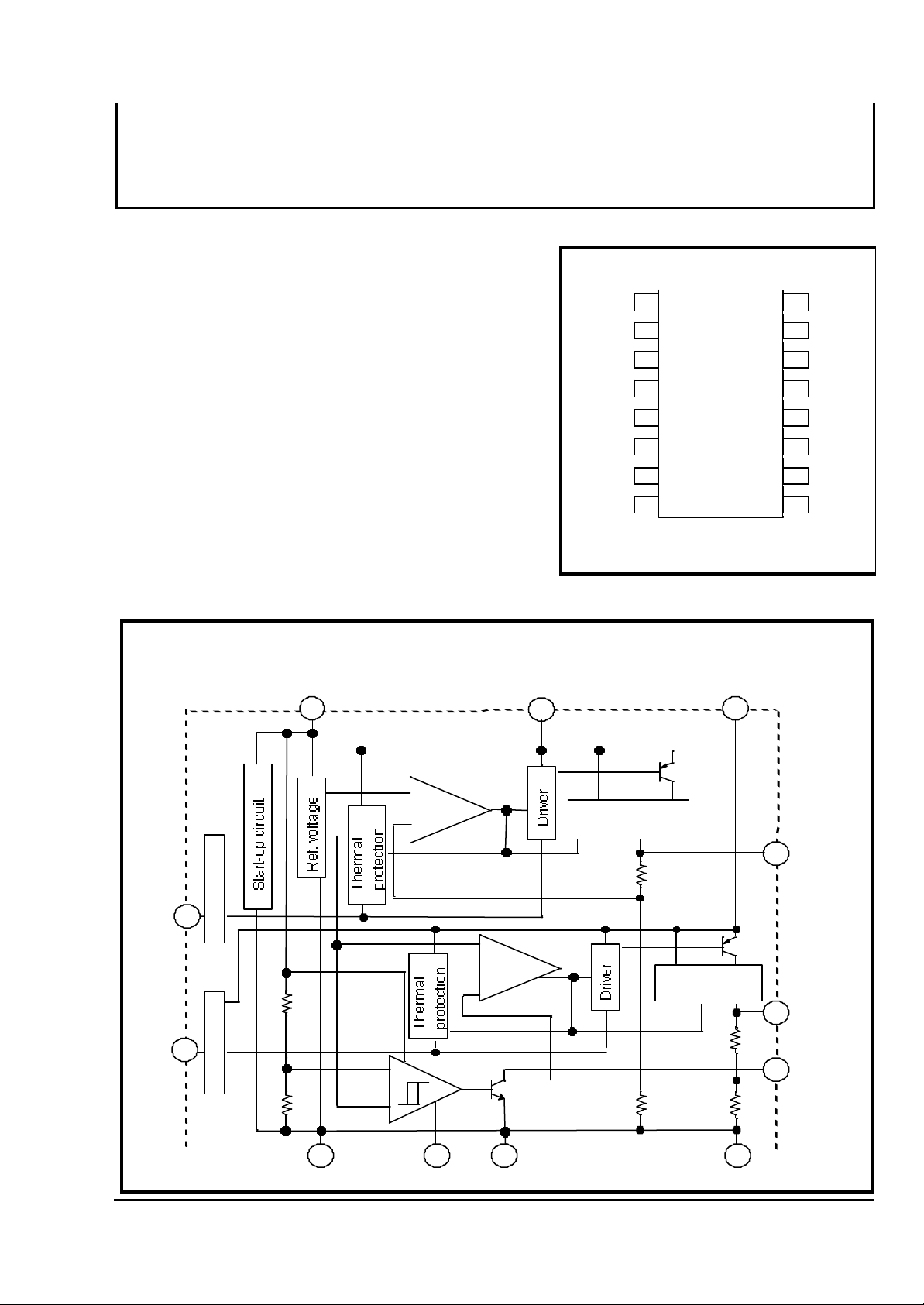
PIN CONFIGURATION(TOP VIEW)
1
VIN1
2
3
GND
4
VIN3
5
NC
6
7
8
VIN2 NC
Outline 16P2N-A
16
15
14
13
12
11
10
9
NC
NC
GND
Cd
GND
CH1
ON/OF
F
CH2
ON/OF
F
Note:Same voltage should be applied to VIN1,VIN2,and VIN3.
GND terminals(4pin, 11pin, 14pin) should be put together
VIN3
5
O
N
/
O
F
2
F
O
N
/
O
7
F
F
to be connected to GND.
+
Err.
Amp.
-
+
Err.
Amp.
VIN1
1
-
-
Overcurrent limit
circuit
Overcurrent limit
circuit
VIN2
8
15
10
3
Output1
Output2
Reset
output
GND
+
4
12 11
Cd
( /4)
1
13
GND
GND
000530

MITSUBISHI<Standard LinearICs>
mWºCºC
300VmAmAV
VmVdB
mV
mAVmVµsV
V
100
200
80
20
10
0.3
IL=150mA
3.3
3.234
3.366
40
120
30
90
RL=2.2kΩ
RL=100kΩ
0.7
0.8
2.55
Cd=0µF
VOUT1+0.3
8
-0.3
0.4VV
V
µA
mV
20
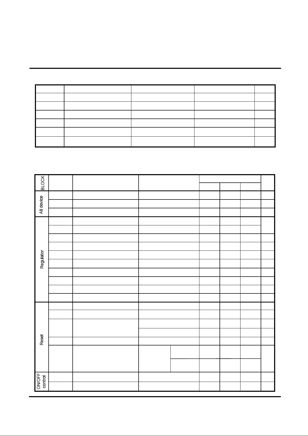
ABSOLUTE MAXIMUM RATINGS(Ta=25ºC,unless otherwise noted.)
ELECTRICAL CHARACTERISTICS(Ta=25ºC, VIN=5V, CI=10µF, Co1=Co2=47µF, unless otherwise noed.)
PRELIMINARY
Symbol
VIN
IL
Pd
Kθ
Topr
Tstg
Symbol Parameter
VIN
Icc1
Icc2
VOUT1
VOUT2
VIO
Reg-IN
Reg-L1
Reg-L2
VNO
RR
IOS
TCVO
Vs
∆Vs
Parameter
Input voltage
Load current *1
Power dissipation
Thermal derating ratio
Operating temperature
Storage temperature
Supply voltage range
Circuit current
Circuit current at OFF
Output voltage(1ch)
Output voltage(2ch)
Input/output differential
Input regulation
Load regulation(1ch)
Load regulation(2ch)
Output noise voltage
Ripple rejection ratio
Output short holding current
Output voltage temp.coefficient
Detection voltage
Hysterisis voltage
M62525FP
HIGH PRECISION LOW INPUT/OUTPUT DIFFERENTIAL( 3.3V, 2.5V)
FIXED OUTPUT VOLTAGE REGULATOR WITH RESET
Condition Ratings Unit
-0.3~9
790
Max.
mW/ºCTa>25ºC
Unit
µVrms
mV/ºC
6.32
-20~+75
-40~+150
Test conditions
IL=0mA 2.2
VIN=4.4V~5.5V,IL=30mA
IL1=0mA~250mA
IL2=0mA~250mA
BW=10Hz~100KHz
vin=0dBm,f=120Hz,IL=30mA
Ta=-20~75∫C, IL=30mA
60
Limits
Typ.Min.
500VON/OFF1,VON/OFF2=0V
2.52.45
50
0.2
4.03.92 4.08
150
tpd
Vsat
VOPL
VON
VOFF
Delay time
Output saturation voltage
Threshold operating voltage
ON threshold voltage
OFF threshold voltage
VIN=3.5V, Isink=1mA 0.2 0.4
L reset type
minimum supply
voltage for IC
operation
( /4)
2
Vsat<0.4V
=
Vsat<0.4V
=
1.6 VIN+0.3
0.6
ms23Cd=0.1µF
0.7
000530
 Loading...